1. Introduction
The work focuses on the operation and possible implementation of tunable magnetic device in electrical power systems with adaptive features. In the following text, this device is referred to as a ‘tuned inductor’ (TI).
The first group of these electrical systems consists of systems for improving the quality of electricity [
1,
2,
3,
4]. A further possible area of implementation of TI solutions is in static power electronics systems, installed in AC transmission grids, as such systems can increase grid power transfer capability, stability, and controllability, through series and/or shunt compensation. These are known as flexible AC transmission systems (FACTS) [
1,
5,
6]. The third area concerns AC/DC, DC/AC, and DC/DC converters, which allow for shaping of the frequency characteristics of these converters [
7,
8,
9,
10]. However, this work focuses mainly on the application of TIs in the first group of power electrical systems.
The negative effect of nonlinear loads on the operation of a power line, resulting in a lowering of the desired parameter values for the electrical energy [
11], is a widely known and well-documented phenomenon. In view of this, various types of compensators, mainly consisting of different kinds of power filters, are used in these electrical systems as preventive measures [
1,
12,
13,
14]. The main task of these devices is to match the shape of the current at its input to the shape of the current, drawn from the same grid node by other loads. As a result of such compensation process the current, flowing from the power line to the load, should have both a suitable shape and a correct phase relationship with the voltage in the power line node. This process depends on the chosen compensation strategy, relative to the reactive power alone or to the both the reactive and the distortion power [
2,
15,
16,
17].
The operation of a TI represents a new approach to the design of power devices with adaptive compensation. However, in this work the operation of an adaptive compensator, as a whole, is not related to any specific power theory. In addition, the use of a TI in these devices is only one example of its possible implementations in the field of electrical power area.
The remainder of the paper consists of five sections, which cover the following issues: the topology of the adaptive passive compensator, the basics of operation of a TI device, a design of the TI, the results of testing a laboratory prototype of electrical power systems with the inductor, and the conclusions.
2. Adaptive Passive Devices for Improving the Quality of Electricity
A fixed-parameter passive compensator improves the power factor of a supply source when its load also has fixed parameters. When these parameters vary, the effectiveness of operation of this type of compensator is lowered [
1,
3,
13,
18], meaning that an adaptive compensator is needed instead. A compensator has adaptive properties if it can be adjusted to changes in both the load power and the power line. This can be carried out by switches or through the use of reactive elements with controllable parameter values. Adaptive compensators can be built in the form of reactive power compensators with semi-controlled devices, such as thyristors, or as switching compensators, commonly known as active power filters (APF), in which different types of fully controlled devices are used in the power stage of the compensator. However, when the load power is very high, as is common for large manufacturing plants, APFs are not usually sufficient.
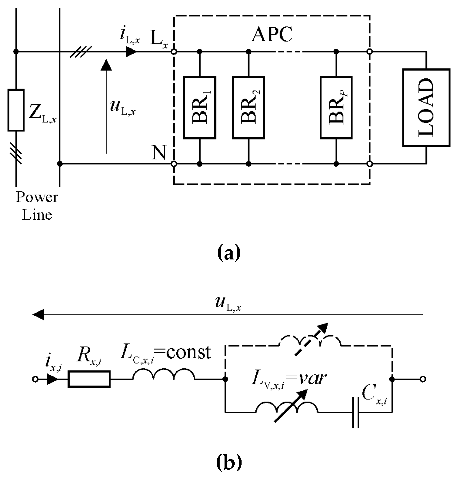
A block diagram of an exemplary electrical system with a generalised adaptive passive compensator (APC) [
1,
3,
13] is shown in
Figure 1a.
The APC contains
branches (
) that can be connected in different ways, typically in parallel, as shown in
Figure 1a. An example of the topology of a single branch, using the TI, is shown in
Figure 1b. As a result of the operation of the tuned inductor, the impedance of this circuit can vary, as follows:
where
is the phase number in the power grid line.
However, it should be clearly stated, that the APC is not, in formal terms, a fully passive system (as follows from its scheme), since this compensator can also use different kinds of single power electronics switches or even complete power electronics converters. These devices are necessary to control TIs, and their role in this type of power system is explained, in detail, in the following section.
3. Principle of Operation of a Tunable Inductive Device
From a formal side, the inductance of the coil is defined by the following formula [
19]:
where:
is the total magnetic flux that is excited in the coil by the current (
), flowing in its winding.
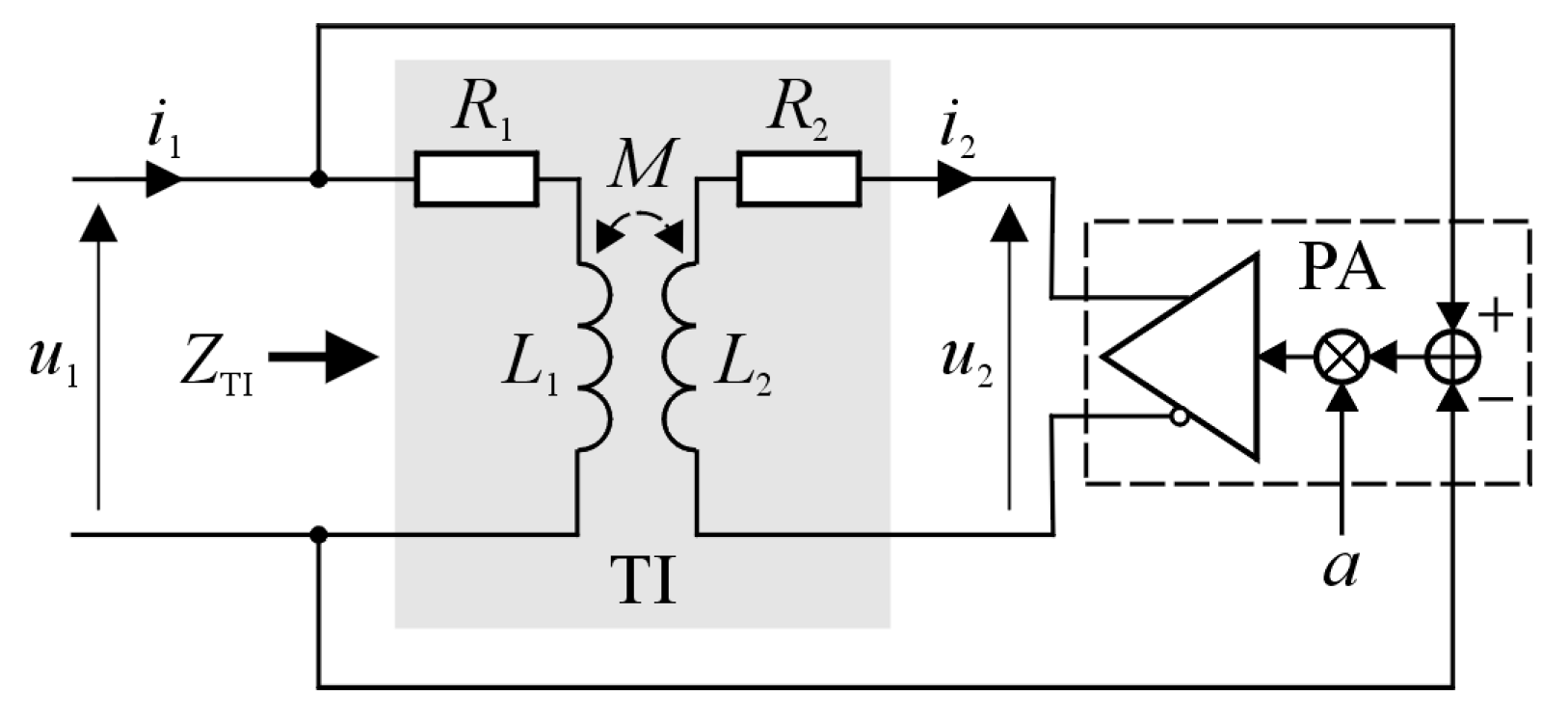
Based on Equation (2), for the implementation of a tunable magnetic device, the circuit with two magnetically coupled coils was used, as shown in
Figure 2.
This circuit consists of two main elements; the first of these is the transformer (TI block), which has a working air-gap in the magnetic core. The width of this air-gap influences the value of the magnetic coupling factor (). The second element is the power amplifier (PA block) with adjustable gain factor (), which powers the secondary winding of the transformer. As a result of the operation of the PA block, the magnetic flux in the core of the transformer can be amplified or weakened, which causes a change in the equivalent impedance () of the circuit, when seen from the power source () side. The value of this impedance depends on the actual values of the parameters of the circuit, and, in particular, the parameter .
The value of the equivalent impedance of this circuit was calculated based on an analysis of the properties of two magnetically coupled circuits [
19]. The initial assumptions made here did not take into account the natural nonlinearity of the ferromagnetic core of the transformer and the voltage excitation (
) was assumed to be sinusoidal.
In this case, the pair of equations, describing the voltage and current relations in the circuit, is as follows:
where:
,
, and
are the self- and mutual reactances of the circuit, respectively and
,
are the resistances of the transformer windings.
Setting
(where
is the PA’s gain factor), the Equations (3) and (4) were transformed to obtain the following formula for the value of
:
where:
From Equations (5) and (6), the following expression was obtained, in which the value of the equivalent impedance (
) is dependent on the other parameters of this circuit:
To extract the
component of the impedance, both resistances were neglected. In this case, Equation (7) taken the form:
Assuming then the equality of both reactances, i.e.
=
=
, Equation (8) has the following final form:
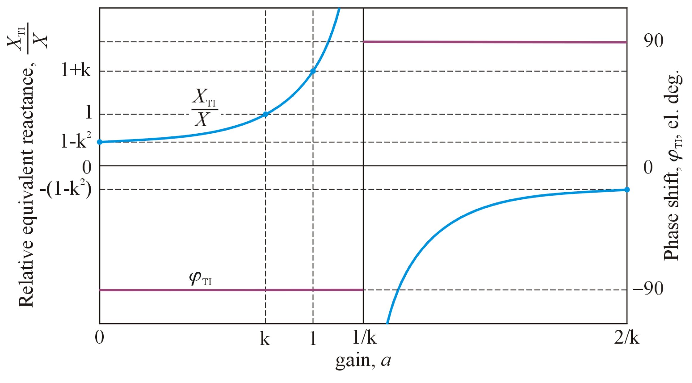
The plots of magnitude (as a value of
, related to
) and phase component (
) of Equation (9), vs.
, while
=const, is shown in
Figure 3. In order to better visualization the details of the curves, the gain factor (
) variation was limited to the range of
. Also, values of reactance, for characteristic values of the gain factor, are shown at the magnitude curve, as points. In relation to the right vertical axis of the chart, the abbreviation “el. deg.” denotes the “electrical degree”.
These curves show singular point at
=
. Thus, the value of
, in relation to the gain factor, lies within intervals given by the expressions:
From circuit theory [
19], the interpretation of Equations (9) and (10) is that, depending on the value of the gain factor, the tunable magnetic device is equivalent to a variable inductance coil or a variable capacitance capacitor. However, in the latter case, it is obvious that it can not form a capacitor as such, because it does not have the ability to store an electric charge. Nevertheless, in a real circuit, that description is given by Equations (5) and (7), and, due to the presence of the resistances, the aforementioned phase shift is different from ±90°. For simplicity, it was assume again the equality of both reactances (
=
=
) and both resistances (
=
=
). In such a case the Equation (7) takes the following form:
For easier interpretation of the circuit features, the time constant of the TI block (
) was used in the next expression. In this case, Equation (11) is as follows:
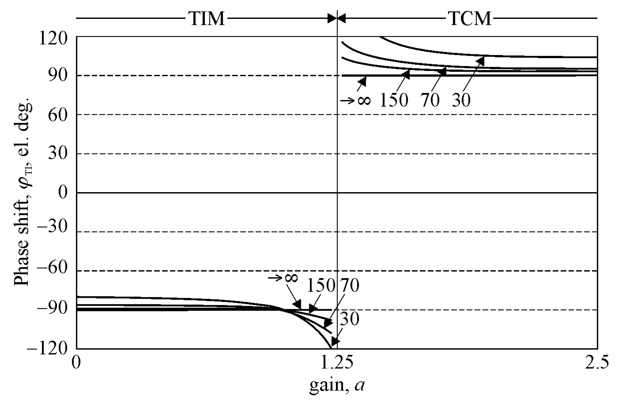
Figure 4 shows the phase shift, based on Equation (12), vs.
, for
= const. The variation in the gain factor was limited to the range
too.
A comparison with
Figure 3b clearly shows phase errors, the values of which increase as the resistance increases which, in turn, results in a decrease in the value of
. From the point of view of the properties of the TI block its operation can be divided into two types, based on the sign of the phase shift. If this sign is negative, the TI operates in the “tuned inductor” mode (TIM), while in the opposite case it operates in the “tuned capacitor” mode (TCM), as illustrated in
Figure 4.
4. Tuned Inductor’s Design
The aim of the research was to obtain technical details of the inductor, which are necessary for the design of its laboratory prototype. At the initial stage, the simulation studies of the TI field model were conducted, using Maxwell Environment [
20] and in-house optimisation software [
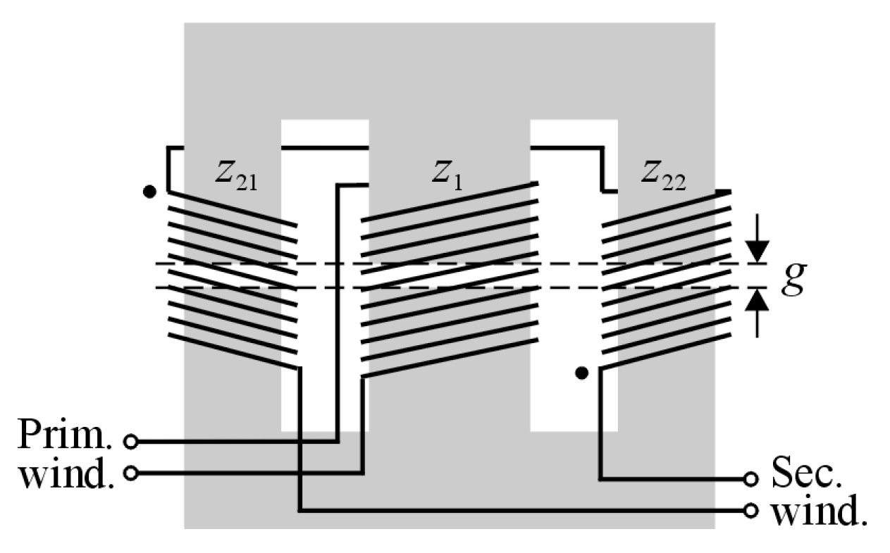
21]. This study showed that, to achieve the assumed value for the inductance of the TI, a sophisticated design of its magnetic circuit was necessary. As a result, a three-column magnetic core was chosen for the model of the transformer. Each of the columns was equipped with a working air-gap with a width equal to
. In the model, ferrite E-shapes, manufactured by MAGNETICS Inc. (catalogue number: OT49928EC), made of T-type ferrite material [
22], were used. The model of the core was composed of four of these shapes. The primary coil was wound on the central column of the device, while the secondary coil was divided into two equal parts and wound on both external columns. To simplify the modelling procedure it was also assumed that the number of turns were equal for all of the coils, i.e.
=
=
, as shown in
Figure 5.
Taking into account the potential fields of application of the TI, reported in previous works [
23,
24], value of
, close to 4.50 mH, and value of
, close to 0.80, were assumed. These aforementioned works also presented details of the whole inductor’s research procedure.
5. Laboratory Tests and Discussion
5.1. Tests of a Laboratory Prototype of the Adjustable Magnetic Device
In the power stage of the tested circuit the P3-5-550MFE LABINVERTER [
25] was implemented. This device was designed for applications in advanced R&D power electronics systems. The control module of the LABINVERTER comprised an ALS-G3-1369 evaluation board [
25] with a 32-bit digital signal processor (DSP) (Analog Devices Inc., ADSP-21369 SHARC
®). In turn, this board is dedicated such power electronics applications, which require a CPU with high computation power and a PWM pattern with high resolution, among others.
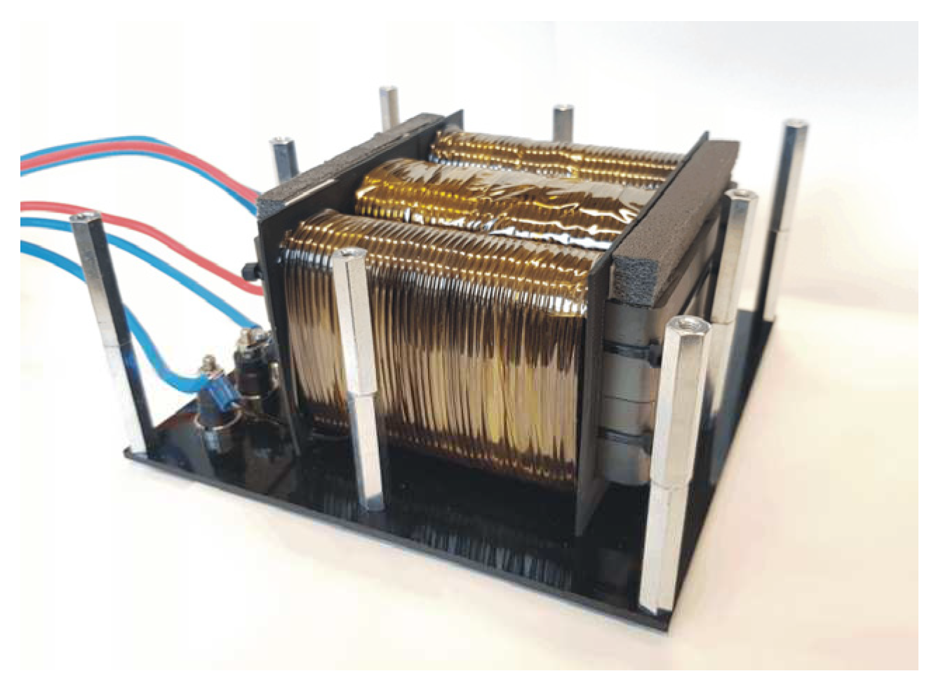
The aim of the first part of the research was to confirm the parameters for the laboratory prototype of TI, in relation to its field model. A photograph of the inductor is shown in
Figure 6.
The methodology used to measure the inductance of TI was described, in detail, in a previous paper [
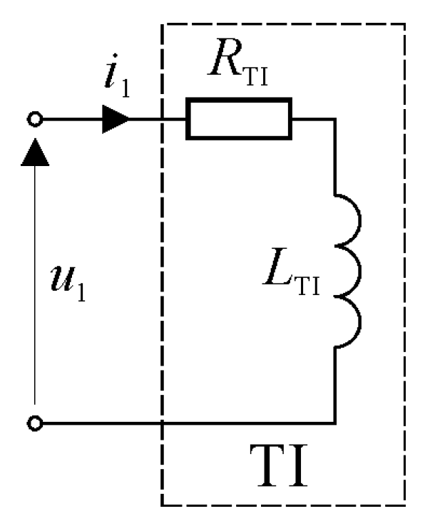
26] so, it is discussed here very briefly, only for the convenience of the reader. This methodology depended on the observation of voltage and current waveforms in the circuit with the TI, as shown in
Figure 7. These waveforms were then used as the basis for calculating the inductance of the TI.
The general formula that describes the voltage and current waveforms in this circuit, in the time-domain, is as follows:
For practical purposes, the resistive component of the circuit was neglected and the supply voltage was assumed to be a rectangular function of time, meaning that the current waveform will be a linear function of time, i.e. a first-order polynomial. As a result, the value of the inductance of the TI can be calculated, using the formula:
where
,
, and
represent the changes in the voltage, current, and time, respectively.
The assumption that neglecting the resistance TI does not result in a significant value of error, when calculating the inductance value, holds true [
26] under the condition that the measurement time-interval (
) is much shorter than the time-constant of this circuit, i.e.:
This statement was confirmed experimentally, based on a wide range of tests of numerous types of inductive devices; the examples of such works are [
23,
24,
26].
As a result of laboratory investigations of the TI model, the following values were obtained for the parameters of this device:
Number of turns: = = = 80;
Air gap width: = 2.0 mm;
Inductance (related to the quasi-linear range of the magnetic core operation) while the secondary winding was open: = 4.55 mH;
Inductance while the secondary winding was short-circuited: = 1.64 mH;
Winding resistance: = 110 mΩ, = 220 mΩ.
Based on these assumptions for the TI model, and from the results of laboratory investigations, the value of the coupling factor was calculated as = 0.80. The relationship between and is then equal to 2.8.
5.2. Tests of the Electrical System with a Tuned Inductor: Basic Configuration
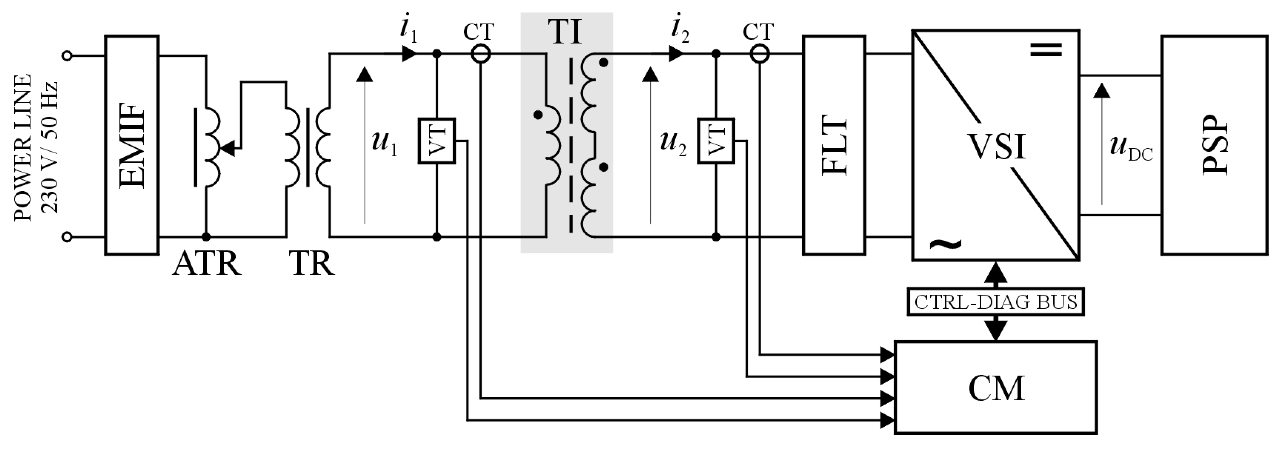
Figure 8 shows a block diagram of the laboratory circuit, used to test the operation of the tuned magnetic device (TI) in the basic configuration. The aim of these tests was to confirm the assumed features of the TI as a tunable magnetic device, i.e., its ability to change the equivalent inductance and more. The measurement circuit consisted of the following main blocks and components:
Power line and EMI filter (EMIF);
Auto-transformer (ATR) and transformer (TR);
Tested magnetic device (TI);
H-bridge, voltage source inverter (VSI);
LCL type filter (FLT), included at the output of the inverter;
Inverter control module (CM);
Isolated current and voltage transducers (CT and VT, respectively);
DC power supply with regulated the output voltage (PSP).
The CM and VSI are interconnected via control & diagnostic bus (CTRL-DIAG BUS). The VSI and FLT blocks made up the precision power electronics voltage controlled voltage source (VCVS), which powered the secondary winding of the transformer (the TI block).
A wide range of tests were carried out on the system with the inductive device, using “hardware-in-the-loop” modelling. Most of the waveforms were recorded, using the PLOT function of DSP Emulator software, which is the part of VisualDSP++
® environment [
27]. The PLOT function allows for graphic visualisation of data, stored as objects in the C/C++ language, such as numerical arrays, typically representing waveforms. A C/C++ compiler is one of the main software components of VisualDSP++. During tests, the gain coefficient of the PA was varied within the interval of <0, 2.5>. During tests, the RMS value of the supply voltage (
) was set to 7 V.
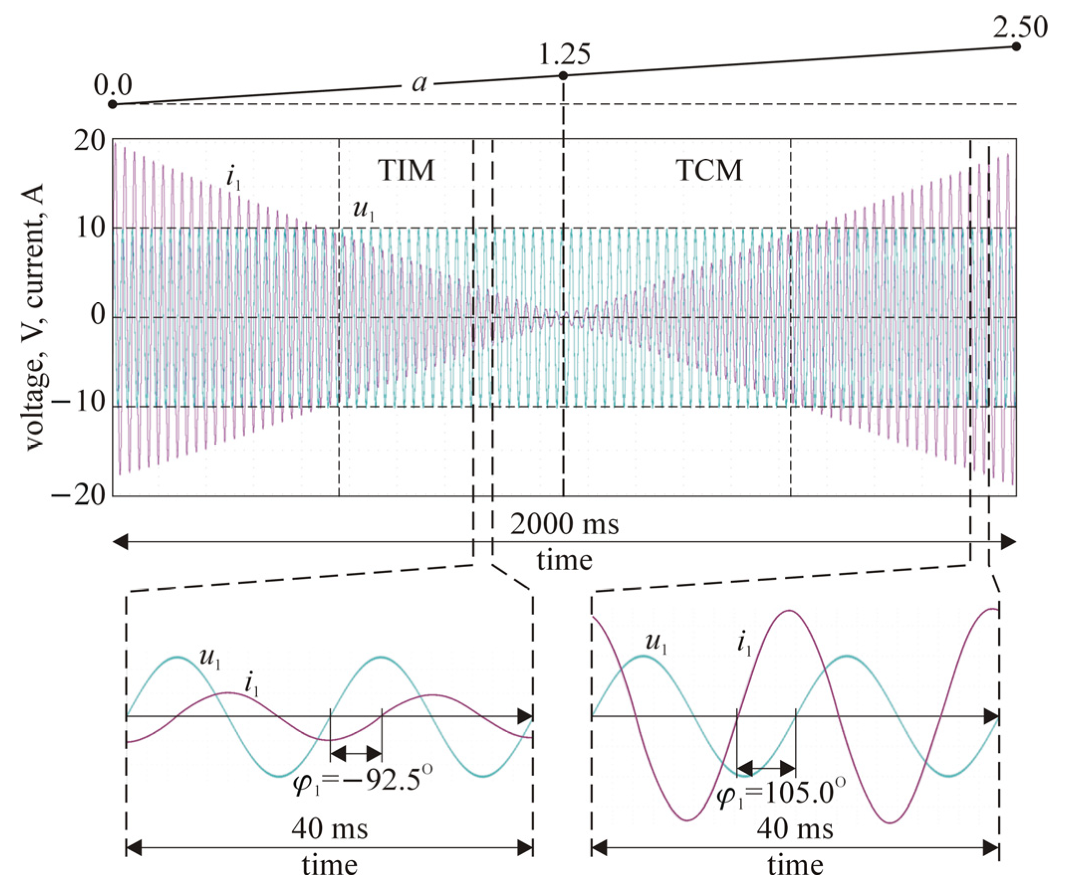
Figure 9 shows the most characteristic waveforms for the tested circuit, i.e.
and
, as function of
, over time. The lower part of this figure shows details of the waveforms, including the phase relationship between these quantities. It can be seen clearly that, after
exceeds the value of
, the circuit changes its character from an inductive to a capacitive one.
5.3. Tests of the Electrical System with a Tuned Inductor: Extended Configuration
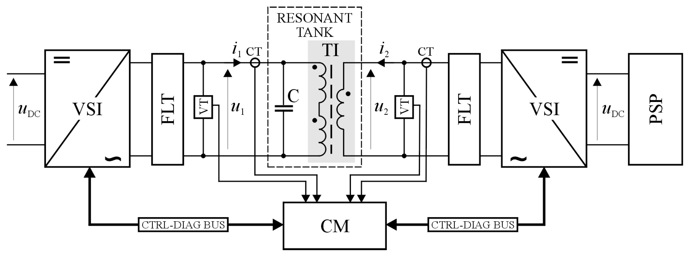
A block diagram of the laboratory circuit used to test the operation of the TI in the extended configuration is shown in
Figure 10. The aim of this part of tests was to confirm the features of the TI as a component of a tunable parallel resonant tank.
The tank (shown in the figure by the dashed line) was composed of TI and capacitive element, consisted of a set of high-quality polypropylene-film capacitors, with total value of C = 300 μF ±1 %. The gain coefficient of the PA was varied in the interval of <0, 1.25>. During these tests, the RMS value of the supply voltage () was set to 10 V and its basic frequency was equal to 150 Hz (i.e., the third harmonics of the power line voltage). Thus, the measurement circuit was demanded implementation of the second VCVS block.
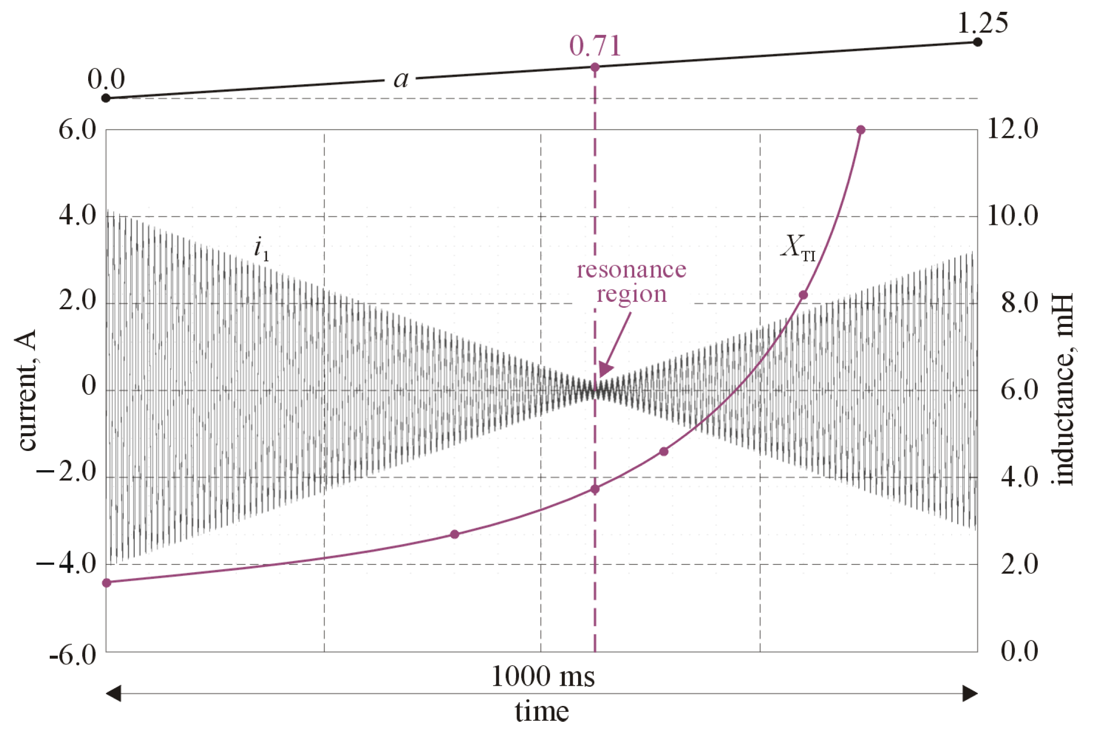
Figure 11 shows both the characteristic waveform for the circuit (
) and the plot of
, vs. time. A curve of the equivalent inductance, vs.
is also shown. From the figure, the moment at which parallel resonance occurs is clearly visible. This results from the given value of the equivalent inductance (reactance) of the TI, which is a function of
.
5.4. Discussion
The test results showed that, from the point of view of the relationship between the voltage and current, the inductive device presented here is able to operate in two modes, as either a tuned inductor or a tuned capacitor. However, the actual values of the equivalent inductance (“capacitance”) of TI were affected by an error of up to 15.0%. The value of this error depends on the gain coefficient, which may result in a decrease in the equivalent reactance of the device. The error arises from factors such as the presence of resistance in the real circuit, the difference between the theoretical and actual voltage values in the secondary circuit of the transformer (caused by the gain error of the power amplifier), and the presence of a ripple component in this voltage, which is caused by the pulse-width modulation (PWM), used to control the power electronics inverters. The phase shift of the primary current from the supply voltage is different from the desired value (i.e., −90° or +90°, depending on the mode of operation of the device), since the circuit contains, among others, the aforementioned TI winding resistances. The value of the phase error was in the range of 2.7–16.7%, depending on the actual value of the gain coefficient. Nevertheless, these tests proved that the proposed device can be an effective element of a tunable resonant tank, by determining its main property, in the form of the value of the self-resonance frequency. In this case, the error in the value of the resonance frequency as a function of the gain factor was no greater than 1% of its expected (theoretical) value. This is within the range of error of the measuring instruments used. It should be noted that, in the simplified version, the tunable inductive device was tested in a real electrical system, including the DC power supply, equipped with the function of active compensation of reactive and distortion power [
24].
Taking into account tests results (especially, included in the
Section 5.2) it can be concluded that the operation of the magnetic element presented in this work is similar to that of a gyrator [
28], as an inverter of impedance.
6. Conclusions
The work presents the principles of operation and test results for model of electrical systems including a variable inductance device. The operation of the device was based on the interaction between a pair of coupled fluxes, but without relying on the natural nonlinearity of the ferromagnetic circuit, as in most previous studies (e.g., [
19]). Instead, the interaction between two magnetic fluxes, in the quasi-linear range of operation of the ferromagnetic core, was exploited. Experimental results confirmed the possibility of obtaining the desired reactance value in a smooth manner, as a result of controlling the flux in the inductor, with relative error of no more than 15%. In the author’s opinion, this value can be considered satisfactory, in view of the high complexity of both the magnetic circuit of the device and the entire system with this device. In addition, tests of a tunable resonant tank confirmed the utility of this device in a power electrical system. Nevertheless, further investigations of the inductor are necessary, to assess the impact of non-linearity of the real magnetic core and power loss on its operation.
Assuming, it seems that the proposed device offers an attractive solution, particularly for electrical power systems with adaptive features, such as those used to improve the quality of electricity and for energy transmission via power lines. However, these applications for the inductor also need further research, using simulation and laboratory models.
List of acronyms
| APC |
Adaptive Passive Compensator |
| APF |
Active Power Filter |
| PA |
Power Amplifier |
| TCM |
Tuned Capacitor Mode |
| TI |
Tuned Inductor |
| TIM |
Tuned Inductor Mode |
| VCVS |
Voltage Controlled Voltage Source |
References
- Rashid, M.H. Power Electronics Handbook; Elsevier Ltd.: Oxford, UK, 2018. [Google Scholar]
- Akagi, H.; Watanabe, E.H.; Aredes, M. Instantaneous Power Theory and Applications to Power Conditioning; John Wiley & Sons: Hoboken, NJ, USA, 2017; ISBN 9781118362105. [Google Scholar]
- Pasko, M.; Buła, D.; Dębowski, K.; Grabowski, D.; Maciążek, M. Selected methods for improving operating conditions of three-phase systems working in the presence of current and voltage deformation—Part I. Arch. Electr. Eng. 2018, 67, 591–602. [Google Scholar] [CrossRef]
- Trinh, Q.; Lee, H. An enhanced grid current compensator for grid-connected distributed generation under nonlinear loads and grid voltage distortions. IEEE Trans. Ind. Electron. 2014, 61, 6528–6537. [Google Scholar] [CrossRef]
- Hamdy, M.; Abdelaziz, A.Y.; Ray, P.; Attia, M.A. Comparison between flexible AC transmission systems (FACTs) and filters regarding renewable energy systems harmonics mitigation. Int. J. Emerg. Electr. Power Syst. 2021, 23, 211–220. [Google Scholar] [CrossRef]
- Benchabira, A.; Khiat, M. A hybrid method for the optimal reactive power dispatch and the control of voltages in an electrical energy network. Arch. Electr. Eng. 2019, 68, 535–551. [Google Scholar] [CrossRef]
- Yang, Y.; Ma, J.; Ho, C.; Zou, Y. A new coupled-inductor structure for interleaving bidirectional DC-DC converters. IEEE J. Emerg. Sel. Top. Power Electron. 2015, 3, 841–849. [Google Scholar] [CrossRef]
- Yang, C.; Liu, Y.; Tseng, P.; Pan, T.; Chiu, H.; Lo, Y. DSP-based interleaved buck power factor corrector with adaptive slope compensation. IEEE Trans. Ind. Electron. 2015, 62, 4665–4677. [Google Scholar] [CrossRef]
- Onal, Y.; Sozer, Y. Bridgeless SEPIC PFC converter for low total harmonic distortion and high power factor. In Proceedings of the Applied Power Electronics Conference and Exposition (APEC), Long Beach, CA, USA, 20–24 March 2016; pp. 2693–2699. [Google Scholar] [CrossRef]
- Liu, J.; Xu, W.; Chan, K.W.; Liu, M.; Zhang, X.; Chan, N.H.L. A Three-phase single-stage AC–DC wireless-power-transfer converter with power factor correction and bus voltage control. IEEE J. Emerg. Sel. Top. Power Electron. 2020, 8, 1782–1800. [Google Scholar] [CrossRef]
- Masetti, C. Revision of European Standard EN 50160 on power quality: Reasons and solutions. In Proceedings of the 14th International Conference on Harmonics and Quality of Power-ICHQP, Bergamo, Italy, 26–29 September 2010. [Google Scholar] [CrossRef]
- Popescu, M.; Bitoleanu, A.; Linca, M.; Suru, C.V. Improving power quality by a four-wire shunt active power filter: A case study. Energies 2021, 14, 1951. [Google Scholar] [CrossRef]
- Czarnecki, L.; Almousa, M. Adaptive balancing by reactive compensators of three-phase linear loads supplied by nonsinusoidal voltage from four-wire lines. Am. J. Electr. Power Energy Syst. 2021, 10, 32–42. [Google Scholar] [CrossRef]
- Ye, T.; Dai, N.; Zhu, M. Optimise the series LC design of a quasi-proportional-resonant controlled hybrid active power filter for harmonic compensation. In Proceedings of the 11th Conference on Industrial Electronics and Applications (IEEE ICIEA), Hefei, China, 5–7 June 2016; pp. 624–629. [Google Scholar] [CrossRef]
- Depenbrock, M.; Marshal, D.A.; Wyk, J.D. Formulating requirements for universally applicable power theory as control algorithm in power compensators. Eur. Trans. Elect. Power ETEP 1994, 4, 445–456. [Google Scholar] [CrossRef]
- Qiao, X.; Bian, J.; Chen, C.; Li, H. Comparison and analysis of reactive power compensation strategy in power system. In Proceedings of the IEEE Sustainable Power and Energy Conference (IEEE iSPEC), Beijing, China, 21–23 November 2019; pp. 689–692. [Google Scholar] [CrossRef]
- Benysek, G.; Pasko, M. (Eds.) Power Theories for Improved Power Quality; Springer-Verlag: London, UK, 2012. [Google Scholar]
- Lee, Y.; Song, H. A reactive power compensation strategy for voltage stability challenges in the Korean power system with dynamic loads. Sustainability 2019, 11, 326. [Google Scholar] [CrossRef]
-
Magnetic Circuits and Transformers: A First Course for Power and Communication Engineers. MIT Department of Electrical Engineering, One Broadway 12th Floor Cambridge, MA 02142, USA, November 15, 1977, ISBN: 9780262630634.
- ANSYS Software. Available online: https://www.ansys.com/products/electronics/ansys-maxwell (accessed on 30 December 2022).
- Knypiński, Ł.; Nowak, L.; Demenko, A. Optimisation of the synchronous motor with hybrid permanent magnet excitation system. COMPEL 2015, 34, 448–4552. [Google Scholar] [CrossRef]
- MAGNETICS Inc. Available online: https://www.mag-inc.com/home (accessed on 30 December 2022).
- Gwóźdź, M.; Wojciechowski, R.M. Use of the tuned multi-legs inductor in the device for improving a quality of electric energy. In Proceedings of the LV Symposium on Electrical Machines (SME), Poznań, Poland, 27–28 April 2022; pp. 1–2. [Google Scholar]
- Ciepliński, Ł.; Gwóźdź, M.; Wojciechowski, R.M. Application of a tuned inductor in a DC power supply with an active compensation function. Energies 2022, 15, 6108. [Google Scholar] [CrossRef]
- ALFINE-TIM. Available online: http://analog.alfine.pl/oferta/produkty-alfine/systemy-uruchomieniowe (accessed on 30 December 2022).
- Gwóźdź, M. The application of tuned inductors in electric power systems. Energies 2022, 15, 8481. [Google Scholar] [CrossRef]
- VDSP++ 5.0, Run-Time Library Manual for SHARC® Processors, Revision 1.5; January 2011, Part Number 82-000420-09, Analog Devices, Inc.: Norwood, MA, USA, One Technology Way. Available online: https://www.analog.com/media/en/dsp-documentation/software-manuals/50_21k_rtl_mn_rev_1.5.pdf (accessed on 30 December 2022).
- Deliyannis, T.; Sun, Y.; Kel Fidler, J. Continuous-Time Active Filter Design; CRC Press, 1999; pp. 81–82. ISBN 0-8493-2573-0. [Google Scholar]
|
Disclaimer/Publisher’s Note: The statements, opinions and data contained in all publications are solely those of the individual author(s) and contributor(s) and not of MDPI and/or the editor(s). MDPI and/or the editor(s) disclaim responsibility for any injury to people or property resulting from any ideas, methods, instructions or products referred to in the content. |
© 2023 by the authors. Licensee MDPI, Basel, Switzerland. This article is an open access article distributed under the terms and conditions of the Creative Commons Attribution (CC BY) license (http://creativecommons.org/licenses/by/4.0/).
