Submitted:
04 July 2023
Posted:
06 July 2023
You are already at the latest version
Abstract
Keywords:
1. Introduction
2. Structure optimization of a microfluidic chip.
2.1. Structural modeling of microfluidic chips
2.2. Algorithm design
2.3. Layout calculation optimization
2.4. Routing algorithm optimization
2.5. Adjustment algorithm optimization
2.6. Improved algorithm flow
3. Experimental results and analysis
4. Conclusions
Author Contributions
Funding
Conflicts of Interest
References
- Fu, E.; Wentland, L. A survey of 3D printing technology applied to paper microfluidics. Lab on a chip 2021, 22, 9–25. [Google Scholar] [CrossRef]
- Yin, B.; Yue, W.; Sohan, A.; Zhou, T.; Qian, C.; Wan, X. Micromixer with Fine-Tuned Mathematical Spiral Structures. ACS omega 2021, 6, 30779–30789. [Google Scholar] [CrossRef]
- Yin, B.; Wan, X.; Qian, C.; Sohan, A.; Wang, S.; Zhou, T. Point-of-Care Testing for Multiple Cardiac Markers Based on a Snail-Shaped Microfluidic Chip. Frontiers in chemistry 2021, 9, 741058. [Google Scholar] [CrossRef]
- Yin, B.F.; Wan, X.H.; Yang, M.Z.; Qian, C.C.; Sohan, A. Wave-shaped microfluidic chip assisted point-of-care testing for accurate and rapid diagnosis of infections. Military Medical Research 2022, 9, 8–21. [Google Scholar] [CrossRef]
- Yin, B.; Qian, C.; Wan, X.; Muhtasim Fuad Sohan, A.S.M.; Lin, X. Tape integrated self-designed microfluidic chip for point-of-care immunoassays simultaneous detection of disease biomarkers with tunable detection range. Biosensors & bioelectronics 2022, 212, 114429. [Google Scholar]
- Yin, B.; Wan, X.; Qian, C.; Sohan, A.; Zhou, T.; Yue, W. Enzyme Method-Based Microfluidic Chip for the Rapid Detection of Copper Ions. Micromachines (Basel) 2021, 12, 1380–1390. [Google Scholar] [CrossRef]
- Shin, W.; Kim, H.J. 3D in vitro morphogenesis of human intestinal epithelium in a gut-on-a-chip or a hybrid chip with a cell culture insert. Nature protocols 2022, 17, 910–939. [Google Scholar] [CrossRef]
- Zhang, Y.; Tseng, T.M.; Schlichtmann, U. Portable all-in-one automated microfluidic system (PAMICON) with 3D-printed chip using novel fluid control mechanism. Sci Rep 2021, 11, 19189–19199. [Google Scholar] [CrossRef] [PubMed]
- Aishan, Y.; Funano, S.I.; Sato, A.; Ito, Y.; Ota, N.; Yalikun, Y.; Tanaka, Y. Bio-actuated microvalve in microfluidics using sensing and actuating function of Mimosa pudica. Sci Rep 2022, 12, 7653–7664. [Google Scholar] [CrossRef] [PubMed]
- Gong, J.; Wang, Q.; Liu, B.; Zhang, H.; Gui, L. A Novel On-Chip Liquid-Metal-Enabled Microvalve. Micromachines (Basel) 2021, 12, 1051–1065. [Google Scholar] [CrossRef] [PubMed]
- Im, S.B.; Uddin, M.J.; Jin, G.J.; Shim, J.S. A disposable on-chip microvalve and pump for programmable microfluidics. Lab on a chip 2018, 18, 1310–1319. [Google Scholar] [CrossRef] [PubMed]
- Liu, W.; He, H.; Zheng, S.Y. Microfluidics in Single-Cell Virology: Technologies and Applications. Trends in biotechnology 2020, 38, 1360–1372. [Google Scholar] [CrossRef] [PubMed]
- Peshin, S.; Madou, M.; Kulinsky, L. Microvalves for Applications in Centrifugal Microfluidics. Sensors (Basel, Switzerland) 2022, 22, 8955–8991. [Google Scholar] [CrossRef] [PubMed]
- Hayes, B.; Smith, L.; Kabutz, H.; Hayes, A.C.; Whiting, G.L.; Jayaram, K.; MacCurdy, R. Rapid Fabrication of Low-Cost Thermal Bubble-Driven Micro-Pumps. Micromachines (Basel) 2022, 13, 1634–1655. [Google Scholar] [CrossRef] [PubMed]
- Gao, R.Z.; Hébert, M.; Huissoon, J.; Ren, C.L. µPump: An open-source pressure pump for precision fluid handling in microfluidics. HardwareX 2020, 7, e00096. [Google Scholar] [CrossRef]
- Bao, Q.; Zhang, J.; Tang, M.; Huang, Z.; Lai, L.; Huang, J.; Wu, C. A Novel PZT Pump with Built-in Compliant Structures. Sensors (Basel, Switzerland) 2019, 19, 1301–1316. [Google Scholar] [CrossRef]
- Tang, P.C.; Eriksson, O.; Sjögren, J.; Fatsis-Kavalopoulos, N.; Kreuger, J.; Andersson, D.I. A Microfluidic Chip for Studies of the Dynamics of Antibiotic Resistance Selection in Bacterial Biofilms. Frontiers in cellular and infection microbiology 2022, 12, 896149. [Google Scholar] [CrossRef]
- Reyes, D.R.; van Heeren, H. Proceedings of the First Workshop on Standards for Microfluidics. Journal of research of the National Institute of Standards and Technology 2019, 124, 1–22. [Google Scholar] [CrossRef]
- Tian, L.L.; Li, C.H.; Ye, Q.C.; Li, Y.F.; Huang, C.Z.; Zhan, L.; Wang, D.M.; Zhen, S.J. A centrifugal microfluidic chip for point-of-care testing of staphylococcal enterotoxin B in complex matrices. Nanoscale 2022, 14, 1380–1385. [Google Scholar] [CrossRef]
- Chantar, H.; Tubishat, M.; Essgaer, M.; Mirjalili, S. Hybrid Binary Dragonfly Algorithm with Simulated Annealing for Feature Selection. SN computer science 2021, 2, 295–306. [Google Scholar] [CrossRef]
- Pei, J.; Xu, L.; Huang, Y.; Jiao, Q.; Yang, M.; Ma, D.; Jiang, S.; Li, H.; Li, Y.; Liu, S.; et al. A Two-Step Simulated Annealing Algorithm for Spectral Data Feature Extraction. Sensors (Basel, Switzerland) 2023, 23, 893–908. [Google Scholar] [CrossRef] [PubMed]
- Benítez-Hidalgo, A.; Nebro, A.J.; Aldana-Montes, J.F. Sequoya: multiobjective multiple sequence alignment in Python. Bioinformatics (Oxford, England) 2020, 36, 3892–3893. [Google Scholar] [CrossRef] [PubMed]
- Meinecke, C.R.; Heldt, G.; Blaudeck, T.; Lindberg, F.W.; van Delft, F.; Rahman, M.A.; Salhotra, A.; Månsson, A.; Linke, H.; Korten, T.; et al. Nanolithographic Fabrication Technologies for Network-Based Biocomputation Devices. Materials (Basel, Switzerland) 2023, 16, 1046–1062. [Google Scholar] [CrossRef] [PubMed]
- Vlaic, S.; Conrad, T.; Tokarski-Schnelle, C.; Gustafsson, M.; Dahmen, U.; Guthke, R.; Schuster, S. ModuleDiscoverer: Identification of regulatory modules in protein-protein interaction networks. Sci Rep 2018, 8, 433–444. [Google Scholar] [CrossRef] [PubMed]
- Valverde, M.G.; Mille, L.S.; Figler, K.P.; Cervantes, E.; Li, V.Y.; Bonventre, J.V.; Masereeuw, R.; Zhang, Y.S. Biomimetic models of the glomerulus. Nature reviews. Nephrology 2022, 18, 241–257. [Google Scholar] [CrossRef] [PubMed]
- Zhang, J.; Tavakoli, H.; Ma, L.; Li, X.; Han, L.; Li, X. Immunotherapy discovery on tumor organoid-on-a-chip platforms that recapitulate the tumor microenvironment. Advanced drug delivery reviews 2022, 187, 114365. [Google Scholar] [CrossRef]
- Cho, S.; Lee, S.; Ahn, S.I. Design and engineering of organ-on-a-chip. Biomedical engineering letters 2023, 13, 97–109. [Google Scholar] [CrossRef]
- Jie, Y. Deep Learning-Guided Simulated Annealing for Designing Vocational High Educational System. Applied bionics and biomechanics 2022, 2022, 7187863. [Google Scholar] [CrossRef]
- Meng, X.; Wang, N.; Liu, J.; Liu, Q. An Improved Simulated Annealing-Based Decision Model for the Hybrid Flow Shop Scheduling of Aviation Ordnance Handling. Computational intelligence and neuroscience 2022, 2022, 1843675. [Google Scholar] [CrossRef]
- Pakela, J.M.; Tseng, H.H.; Matuszak, M.M.; Ten Haken, R.K.; McShan, D.L.; El Naqa, I. Quantum-inspired algorithm for radiotherapy planning optimization. Medical physics 2020, 47, 5–18. [Google Scholar] [CrossRef]
- Leber, A.; Dong, C.; Laperrousaz, S.; Banerjee, H.; Abdelaziz, M.; Bartolomei, N.; Schyrr, B.; Temelkuran, B.; Sorin, F. Highly Integrated Multi-Material Fibers for Soft Robotics. Advanced science (Weinheim, Baden-Wurttemberg, Germany) 2023, 10, e2204016. [Google Scholar] [CrossRef]
- Zeng, W.; Guo, L.; Xu, S.; Chen, J.; Zhou, J. High-Throughput Screening Technology in Industrial Biotechnology. Trends in biotechnology 2020, 38, 888–906. [Google Scholar] [CrossRef]
- Zabihihesari, A.; Hilliker, A.J.; Rezai, P. Fly-on-a-Chip: Microfluidics for Drosophila melanogaster Studies. Integrative biology : quantitative biosciences from nano to macro 2019, 11, 425–443. [Google Scholar] [CrossRef] [PubMed]
- Cheng, C.; Foxworthy, G.; Fridman, G. On-chip ionic current sensor. Applied physics. A, Materials science & processing 2021, 127, 314–324. [Google Scholar]
- Wei, C.; Zong, Y.; Jiang, Y. Bioinspired Wire-on-Pillar Magneto-Responsive Superhydrophobic Arrays. ACS Appl Mater Interfaces 2023, 15, 24989–24998. [Google Scholar] [CrossRef] [PubMed]
- Sakaguchi, K.; Akimoto, K.; Takaira, M.; Tanaka, R.I.; Shimizu, T.; Umezu, S. Cell-Based Microfluidic Device Utilizing Cell Sheet Technology. Cyborg and bionic systems (Washington, D.C.) 2022, 2022, 9758187. [Google Scholar] [CrossRef]
- Ducrée, J. Systematic review of centrifugal valving based on digital twin modeling towards highly integrated lab-on-a-disc systems. Microsystems & nanoengineering 2021, 7, 104–130. [Google Scholar]
- Sanka, R.; Lippai, J.; Samarasekera, D.; Nemsick, S.; Densmore, D. 3DμF - Interactive Design Environment for Continuous Flow Microfluidic Devices. Sci Rep 2019, 9, 9166–9176. [Google Scholar] [CrossRef]
- Honrado, C.; McGrath, J.S.; Reale, R.; Bisegna, P.; Swami, N.S.; Caselli, F. A neural network approach for real-time particle/cell characterization in microfluidic impedance cytometry. Analytical and bioanalytical chemistry 2020, 412, 3835–3845. [Google Scholar] [CrossRef]
- Ross, G.A.; Rustenburg, A.S.; Grinaway, P.B.; Fass, J.; Chodera, J.D. Biomolecular Simulations under Realistic Macroscopic Salt Conditions. The journal of physical chemistry. B 2018, 122, 5466–5486. [Google Scholar] [CrossRef]
- Song, C.; Du, Q.; Yang, S.; Feng, H.; Pang, H.; Li, C. Flexible joint parameters identification method based on improved tracking differentiator and adaptive differential evolution. The Review of scientific instruments 2022, 93, 084706. [Google Scholar] [CrossRef] [PubMed]
- Suh, D.; Radak, B.K.; Chipot, C.; Roux, B. Enhanced configurational sampling with hybrid non-equilibrium molecular dynamics-Monte Carlo propagator. The Journal of chemical physics 2018, 148, 14101–14110. [Google Scholar] [CrossRef] [PubMed]
Disclaimer/Publisher’s Note: The statements, opinions, and data contained in all publications are solely those of the individual author(s) and contributor(s) and not of MDPI and/or the editor(s). MDPI and/or the editor(s) disclaim responsibility for any injury to people or property resulting from any ideas, methods, instructions, or products referred to in the content. |
| Input: sequence pair (SX, SY), width (length) of n devices, width [n] (heights [n]) | |
| Output: x (y) coordinates x_coords (y_coords), the W (H) dimension of the layout structure. | |
| 1. for(i = 1 to n) | |
| 2. weights [i] = widths [i] | //Weight of device-width |
| 3. (x_coords, W) = LCS (SX, SY, weights) | //X coordinate, total width W |
| 4. for(i = 1 to n) | |
| 5. weights [i] = heights [i] | //Weight of device height |
| 6. SXR[i]=SX[n+1-i] | //Reverse SX |
| 7. (y_coords, H) = LCS(SXR, SY, weights) | //Y coordinate, total height H |
| Input: sequences S1 and S2, weights of n devices [n] | |
| Output: position of each module, total length L | |
| 1. for(i =1 to n) | |
| 2. block_order[S2[i]]=i | //Index of each device in S2 |
| 3. lengths[i]=0 | //Total length initialization of all devices |
| 4. for(i=1 to n) | |
| 5. block=S1[i] | //Current device |
| 6. index=block_order[block] | //Index of current device in S2 |
| 7. positions[block]=lengths[index] | //Calculate the position of the device |
| 8. t_span=positions[block]+weights[block] | //Determine the current fast length |
| 9. for(j=index to n) | |
| 10. if(t_span>lengths[j]) | |
| 11. lengths[j]=t_span | //The length of the current device replaces the former |
| 12. else break | |
| 13. L=lengths[n] | //Total length |
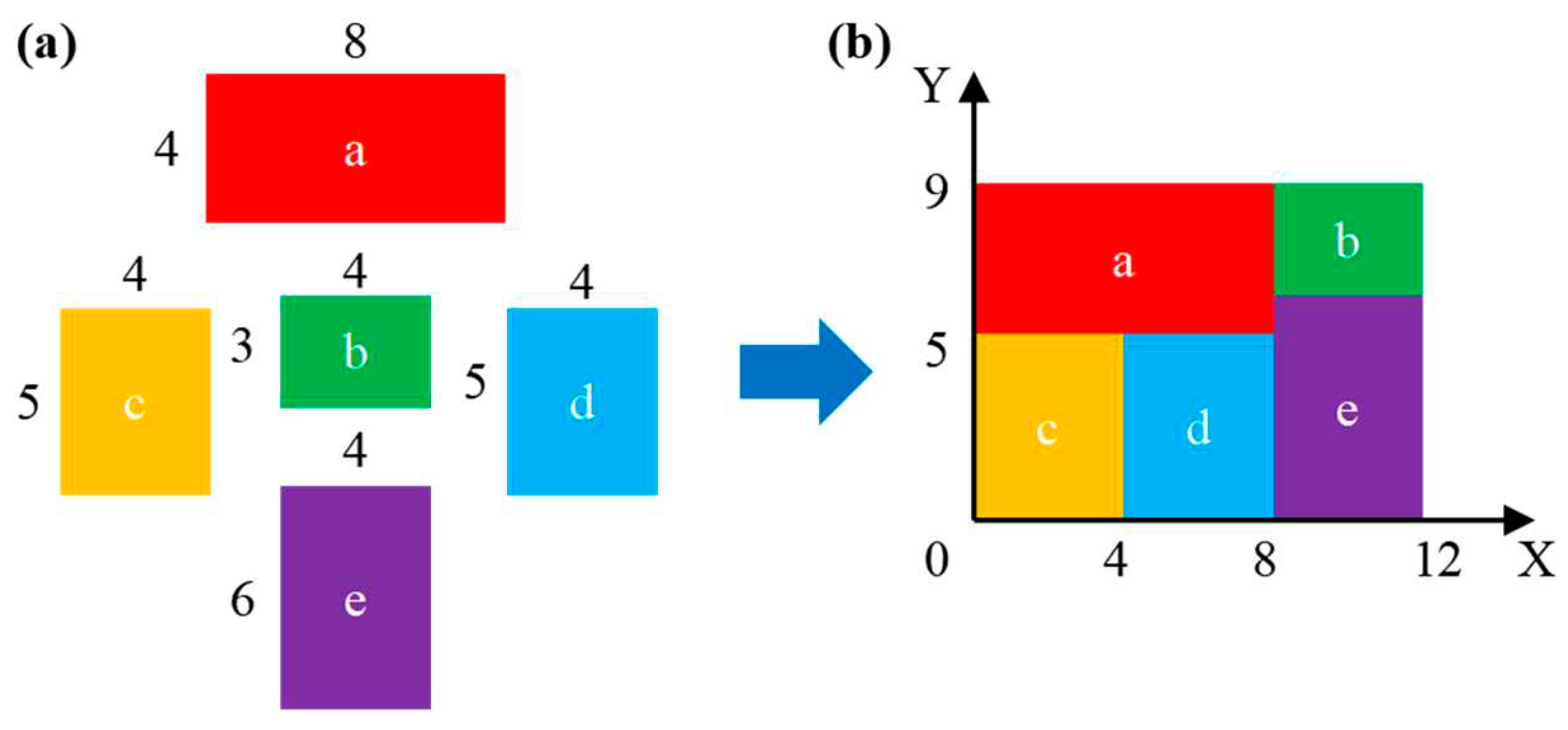
| device | widths | heights |
|---|---|---|
| a | 8 | 4 |
| b | 4 | 3 |
| c | 4 | 5 |
| d | 4 | 5 |
| e | 4 | 6 |
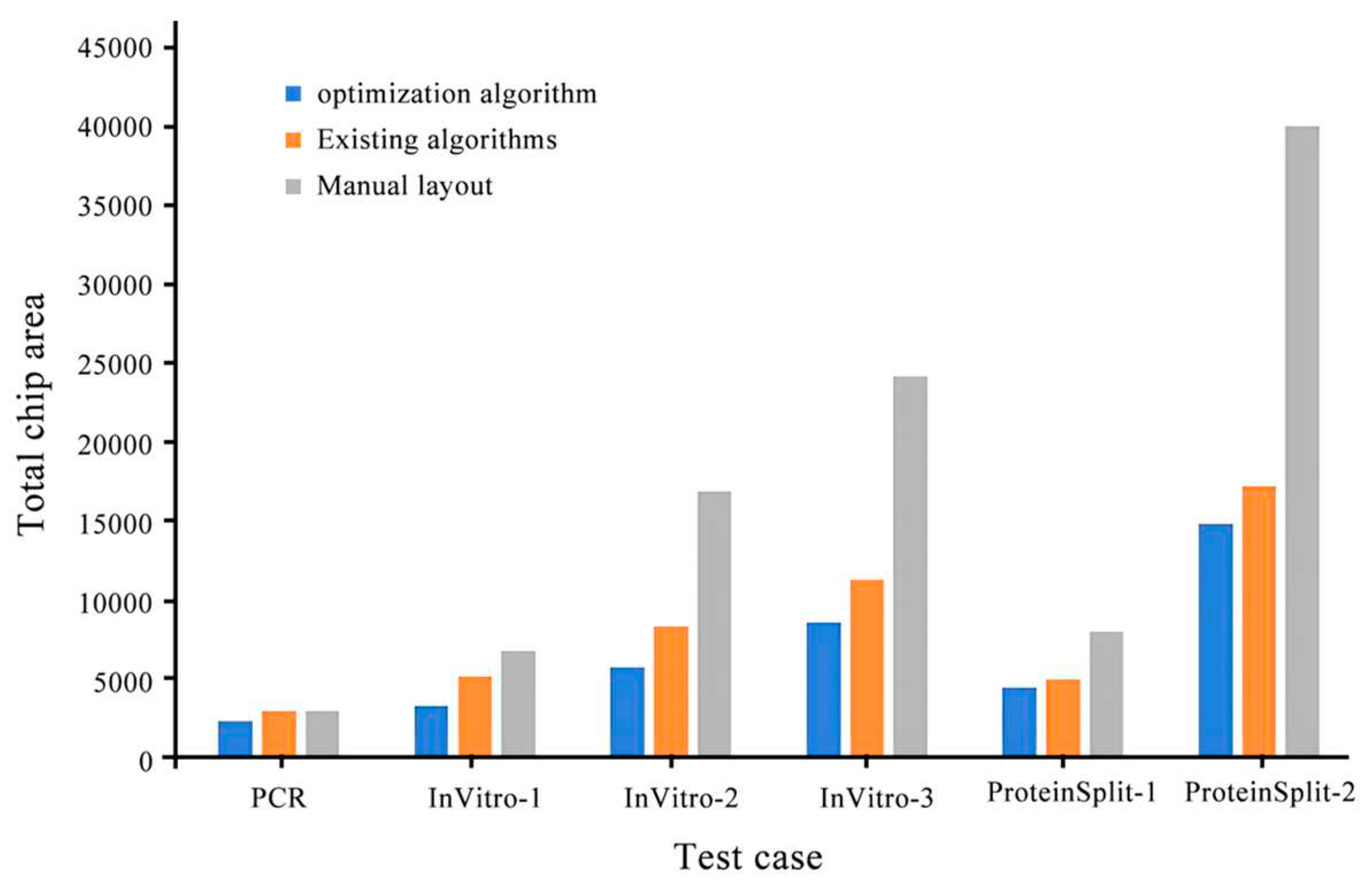
| Test case | Chip area (Existing algorithm/optimization algorithm) |
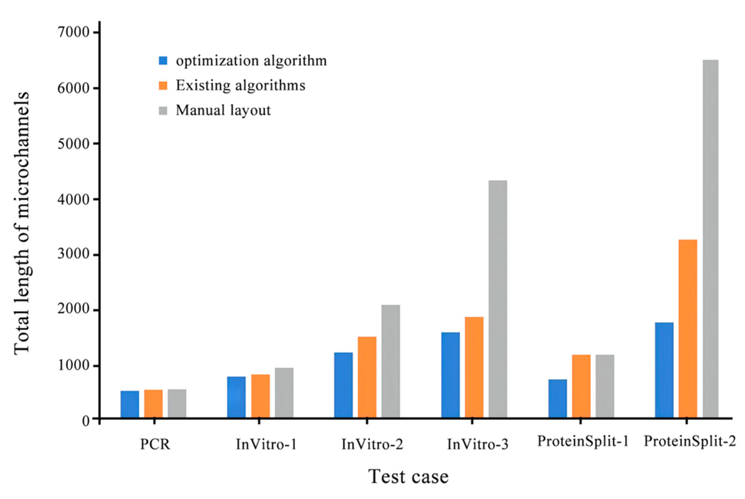
Microchannel length (Existing algorithm/optimization algorithm) |
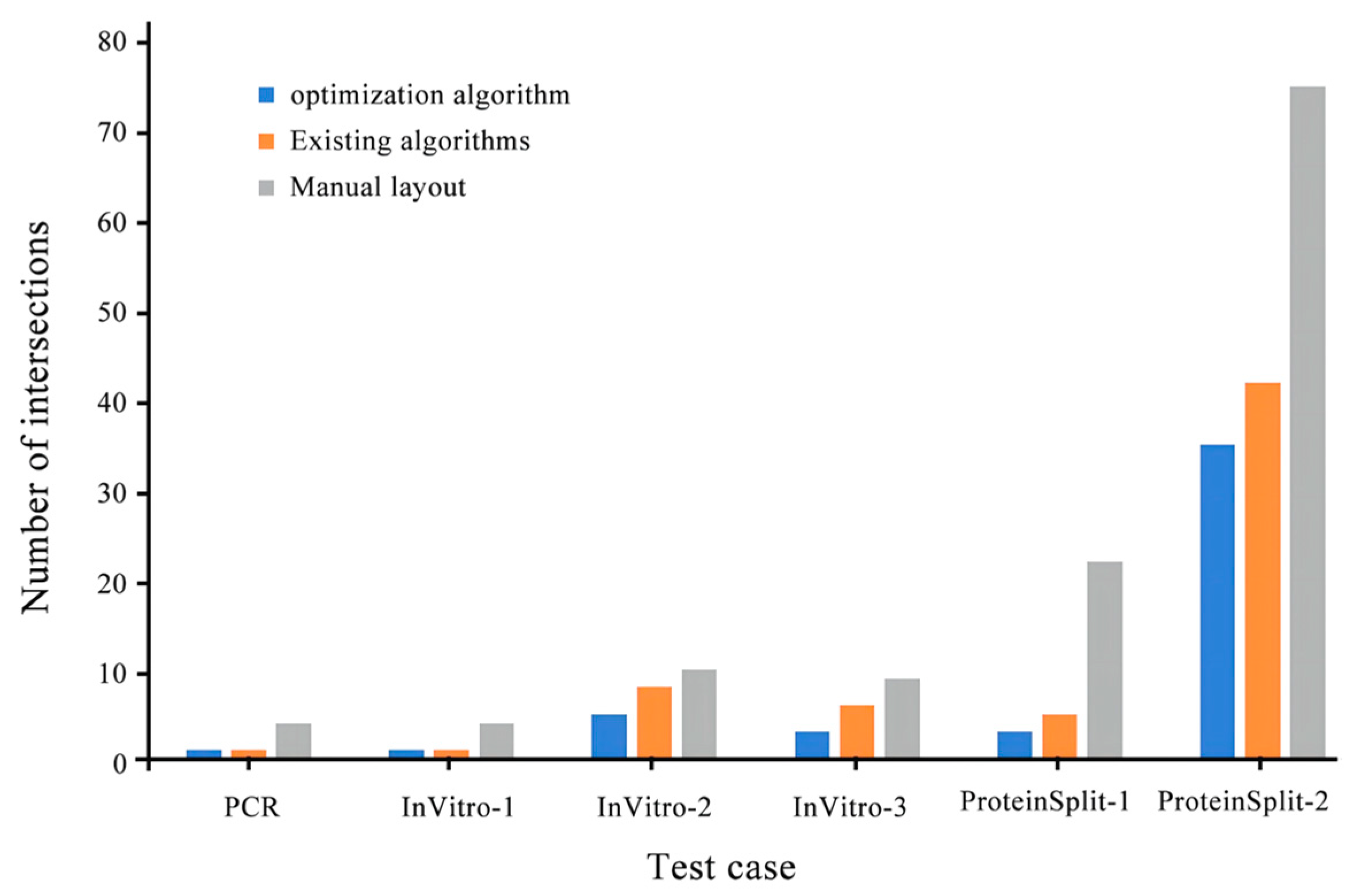
Microchannel intersection (Existing algorithm/optimization algorithm) |
Percent improvement (%) |
|---|---|---|---|---|
| PCR | 2958/2850 | 522/509 | 1/1 | 3.6 |
| InVitro-1 | 5110/3906 | 802/765 | 1/1 | 23.5 |
| InVitro-2 | 8232/5688 | 1485/1203 | 8/5 | 30.9 |
| InVitro-3 | 11187/8460 | 1864/1568 | 6/3 | 24.3 |
| ProteinSplit-1 | 4914/4422 | 1162/713 | 5/3 | 10.0 |
| ProteinSplit-2 | 17030/14690 | 3247/1749 | 42/35 | 13.7 |
Disclaimer/Publisher’s Note: The statements, opinions and data contained in all publications are solely those of the individual author(s) and contributor(s) and not of MDPI and/or the editor(s). MDPI and/or the editor(s) disclaim responsibility for any injury to people or property resulting from any ideas, methods, instructions or products referred to in the content. |
© 2023 by the authors. Licensee MDPI, Basel, Switzerland. This article is an open access article distributed under the terms and conditions of the Creative Commons Attribution (CC BY) license (http://creativecommons.org/licenses/by/4.0/).


