1. Introduction
Power converter technologies play an increasingly important role in many applications mainly because of their capability to efficiently manage the electrical energy [
1]. In this regard, the high penetration of power electronic converters has been justified primarily because of the growth of the electricity generated by renewable energies such as solar and wind [
2]. Since all power converters connected to the grid must fulfil grid codes, power quality has recently become one of the main issues to solve [
3,
4]. A power quality problem can be seen as the divergence of magnitude and frequency from the ideal sinusoidal waveform [
5,
6]. This divergence typically impacts currents and voltage at the grid side and at the load side. In this regards, recently has been proposed in several papers to address the power quality issues to reduce losses and increase the efficiency of the voltage source converter (VSC) [
7,
8]. The dizzying advance of power converters has been enhanced by developing high-performance microprocessors capable of implementing complex nonlinear digital controllers. The field of power electronic semiconductors has recently developed new high-speed switching devices with tremendous low on-state loss. One of the most promising power electronic semiconductors is SiC-MOSFET used in this paper. As a result, new power electronic converters can be smaller than the classical ones [
9].
From the point of view of the conventional AC-DC-AC the two-level voltage source converters (2L-VSCs) are still one of the most used converters for many applications, and nowadays the 2L-VSCs are considered the fundamental component in both industrial applications and renewable energies. However, the reduced number of output voltage levels generate losses problems and poor power quality due to their poor harmonic profile [
10,
11]. To solve this issue, the modular multilevel converter (MMC) has drawn the attention of both industry and energy sectors due to its capability to generate sinusoidal voltages and currents with a low content of harmonic distortions. Among these MMC topologies, the cascade H-Bridge (CHB) based is a popular choice justified mainly by its modularity, which simplifies the extension for a higher number of levels of the MMC. Moreover, MMC does not demand a vast number of flying capacitors or clamping diodes [
12]. Consequently, one of the most widely discussed topologies in the literature are the seven-level voltage source converters (7L-VSCs) based on three CHB cells in serie per phase. [
13]. However, both 2L-VSC and 7L-VSC topologies are based on AC-DC-AC configurations, which requires the inclusion of an intermediate stage of energy storage elements such as capacitor banks. These additional components contribute to increased weight, volume, and above all these capacitors add a possibility of failure in the VSCs. In this sense, recent research efforts have focused on the development of a versatile direct AC-AC power interface that adopts a modular architecture. This innovative approach enables the interconnection of AC sources to the grid and load side without the need for energy storage elements. Within this context, the matrix converter (MC) has emerged as a promising solution. The MC facilitates the generation of a three-phase sinusoidal voltage with adjustable amplitude and frequency by utilizing fully controlled bi-directional switches, eliminating the requirement for energy storage elements [
14].
Among these VSC topologies, the commonly employed power semiconductor devices are IGBTs. However, SiC-MOSFETs have gained attention as an alternative due to their ability to operate at higher switching frequencies compared to IGBTs [
15,
16,
17]. Nevertheless, simply incorporating faster switching devices is insufficient to improve power quality. It is crucial to prioritize the design of the entire converter to ensure enhanced performance at high switching frequencies with power semiconductor devices [
18,
19]. This article presents a comprehensive approach to the design of voltage source converters, focusing particularly on three types of converters based on SiC-MOSFET semiconductor devices. This article is divided as follows.
Section 2 introduces the H-Bridge cells design. Then, in
Section 3, the 2L-VSCs based on CHB cells in paralell configuration is presented, and the experimental result under fault condition are analyzed. In
Section 4, the 7L-VSCs topology is addresses. In
Section 5 the MC design and experimental results are presented. Finally, the main conclusions of this work are given in the last section.
2. H-Bridge cell based converters
In recent years, the trend in power electronics design has shifted towards modular solutions. Modularity enables the scalability of the converter, allowing for an increase in power capacity by arranging several H-Bridge cells in parallel. Alternatively, assembling cells in series can result in a multilevel converter. A modular design for an H-Bridge cell must consider various aspects, such as the switching signals of the power semiconductors, the generation of dead times, and the implementation of protection circuits. These considerations are essential to provide robustness to the H-Bridge cell and ensure its reliable operation. Furthermore, the use of a modular approach can also simplify maintenance and repair processes, as individual cells can be replaced if necessary, without affecting the entire system. Overall, the modular design approach offers several advantages, including scalability, robustness, and ease of maintenance, making it a popular choice for power converter design [
20].
2.1. Switching signal drivers
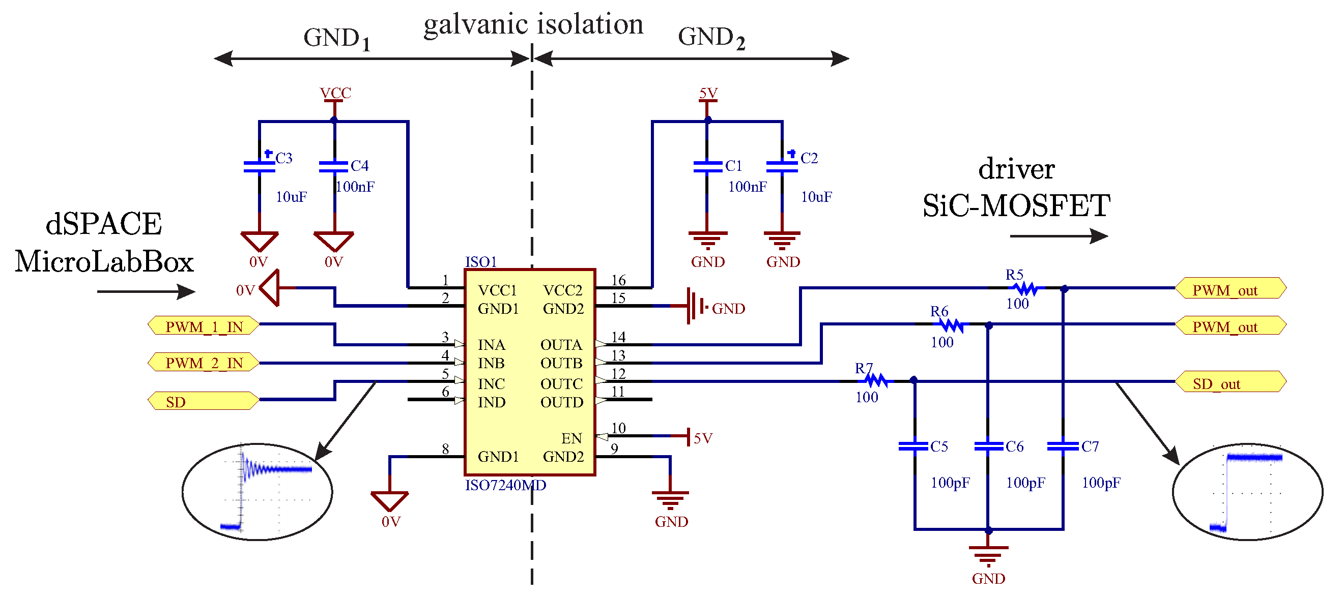
The switching signal drivers are an essential component in the control circuit of SiC-MOSFETs semiconductor devices, they ensure the proper operation of the power conversion system. However, these drivers are susceptible to the electrical noise generated by the high-frequency switching of the power semiconductor devices. To overcome this issue, it is necessary to incorporate a galvanic isolation stage in the driver circuit. This galvanic isolation stage helps in achieving immunity to electrical noise and ensures the stable operation of the power conversion system. The driver circuit, as shown in
Figure 1, exhibits an under damped characteristic of the input signal from the control module to the galvanic isolator. To compensate for this under damping, a passive low-pass filter is used. The design of this filter takes into consideration the maximum switching frequency of the power semiconductor device, and it helps in reducing the noise and improving the performance of the driver circuit.
2.2. Dead time generation circuit
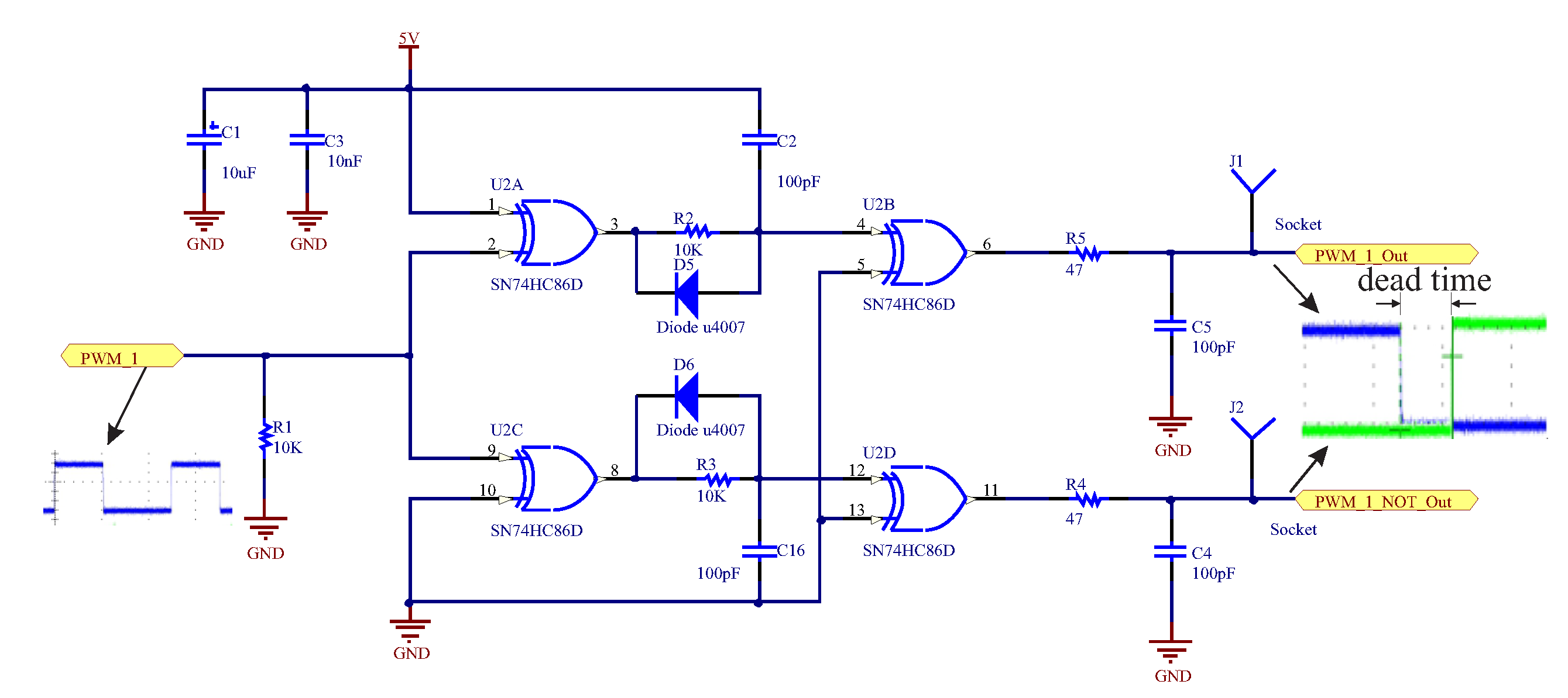
In addition to galvanic isolation, it is also crucial to implement dead time in the complementary signals applied to the half-h-bridge. Dead time is a brief interval where both switches in the half-h-bridge are turned off to avoid short circuits between edge changes of the switching signals [
21]. This ensures that the output voltage is always proportional to the control signal and reduces the likelihood of power device failure due to short circuits.
Figure 2 displays the driver circuitry, where the application of dead time is evident in the complementary signals [
22]. The input signal from the control module to the galvanic isolator exhibits an under damped characteristic, which is compensated for by the use of a passive low-pass filter. The filter is designed to suppress high-frequency noise generated by the switching of the power semiconductor device, while considering the maximum switching frequency.
2.3. Gate complementary signals generation
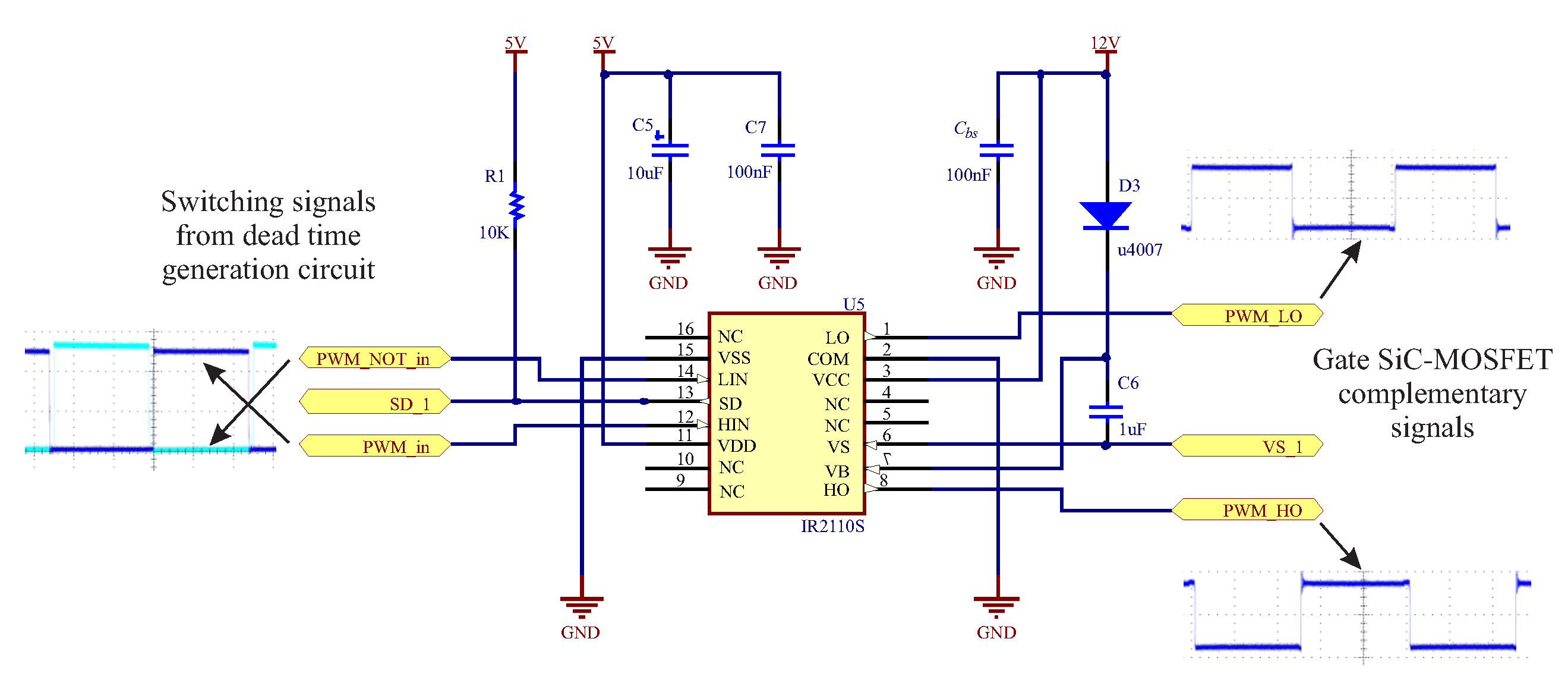
The IR2110S device, as a high voltage, high speed power MOSFET and IGBT driver with independent high and low side referenced output channels, is crucial in properly driving the high-side devices of a bridge circuit, as well as the low-side devices. As shown in
Figure 3, the gate driver circuit employs a bootstrap circuit, which provides the required voltage to the high-side devices. Specifically, the bootstrap capacitor C1 is charged by the voltage across the low-side device and then used to switch the high-side device [
23]. The advantage of this configuration is that it allows for the use of a single isolated power supply for the driver circuit, thereby reducing the overall system complexity and cost. Moreover, the IR2110S device incorporates an under-voltage lockout function, which ensures that the power MOSFETs and IGBTs are not damaged due to insufficient voltage levels, thus improving the reliability of the circuit.
2.4. H-Bridge cell experimental test
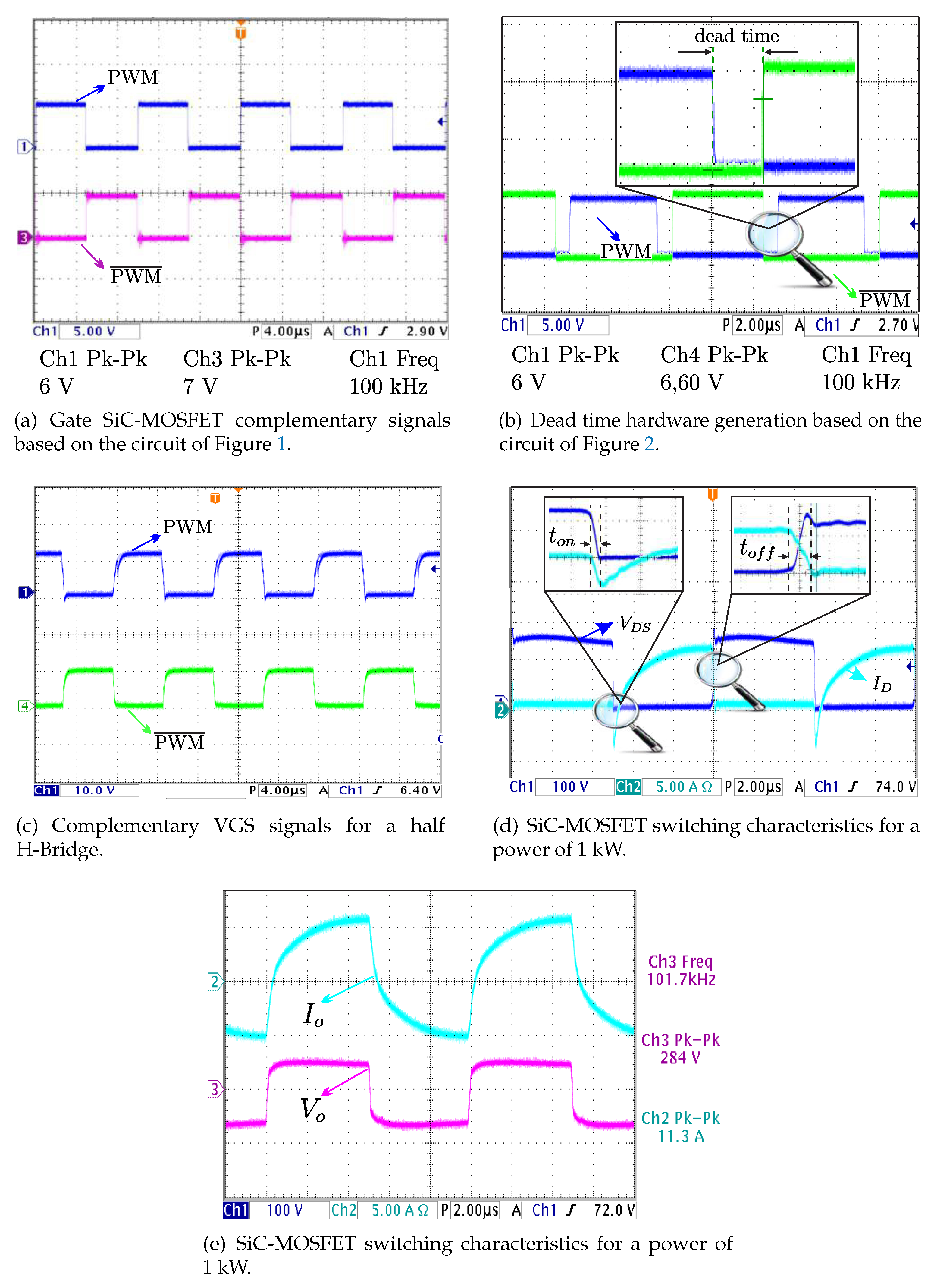
In the oscillogram of
Figure 4 (a), the output signals
and
from the signal conditioner can be observed. As can be seen, the
and
signals do not present overshoots or oscillations, mainly due to the action of the low-pass RC filter, although they do present a slight attenuation in amplitude due to the signal passing through the filter. However, this last characteristic does not affect the general operation of the triggering system. Subsequently, the
and
signals obtained from the conditioning circuit pass to the block in charge of generating the complements of each branch of the H-Bridge cell, to then generate the dead time. This generation of dead time can be observed in the oscillogram of
Figure 4 (b), where an enlargement of the signal graph can also be appreciated for a better identification of the dead time generation. The measured value of the dead time is approximately 1
s for a switching frequency of 100 kHz. The dead time is obtained by a circuit composed of logic gates from the 74HC86 series and combined with resistive and capacitive elements.
The complementary PWM signals generated by the control circuits implemented using the IR2110S integrated circuit are sent to each SiC-MOSFET device to perform the corresponding switching. Each IR2110S integrated circuit controls one branch of a H-Bridge, so two IR2110S are required to implement a cell. In the oscillogram of
Figure 4 (c), the trigger signals can be observed, which have a delay time during the high and low transitions. These delays are due to the input parasitic capacitances of the SiC-MOSFET devices, which, together with the resistance
, form a low-pass filter that produces a slight distortion of the control signal. On the other hand, to analyze the switching characteristics, it is necessary to measure the current signals
and voltage signals
on the power device. Desirable characteristics such as reduced overshoot or oscillations are observed. These characteristics can be seen in the oscillogram of
Figure 4 (d), where a simultaneous representation of the voltage (
) and current (
) signals can be observed.
The output voltage (
) and output current (
) are shown in the oscillogram of
Figure 4 (e). It can be observed that the signal
has a smoother transition between high and low levels compared to the output voltage (
), mainly due to the inductive nature of the load connected to the converter for performing the preliminary experimental tests. It can be seen that the output signals do not present significant overshoot or oscillations, therefore their response is as expected for the type of load considered during the test.
3. Two-level multi modular VSC topology
The scalable 2L-VSC topology consists of parallel-connected H-bridge cells, as shown in the schematic of
Figure 5 (a). The modular characteristic makes it particularly useful for applications where a compact converter, high energy density, and good reliability are required. This is possible by incorporating a redundant scheme, constituting an advantage compared to conventional converters. The following characteristics: simple and compact power circuit, scalability in terms of nominal power and possibility of operation in the event of faults due to redundancy of modules connected in parallel, result in a more robust, economical and flexible VSC compared to traditional configurations.
From the point of view of the power semiconductor devices, SiC-MOSFETs have a comparative advantage in terms of switching losses and switching frequencies, compared to IGBT-type semiconductor devices. The implemented scalable multi-modular 2L-VSC which is shown in
Figure 5 (b) integrates SiC-MOSFET-type semiconductors, and its switching hardware has been designed to achieve switching frequencies close to 100 kHz.
3.1. Two-level multi modular VSC experimental results
The parameters used in the experimental test bench of the 2L-VSC are shown in
Table 1. In
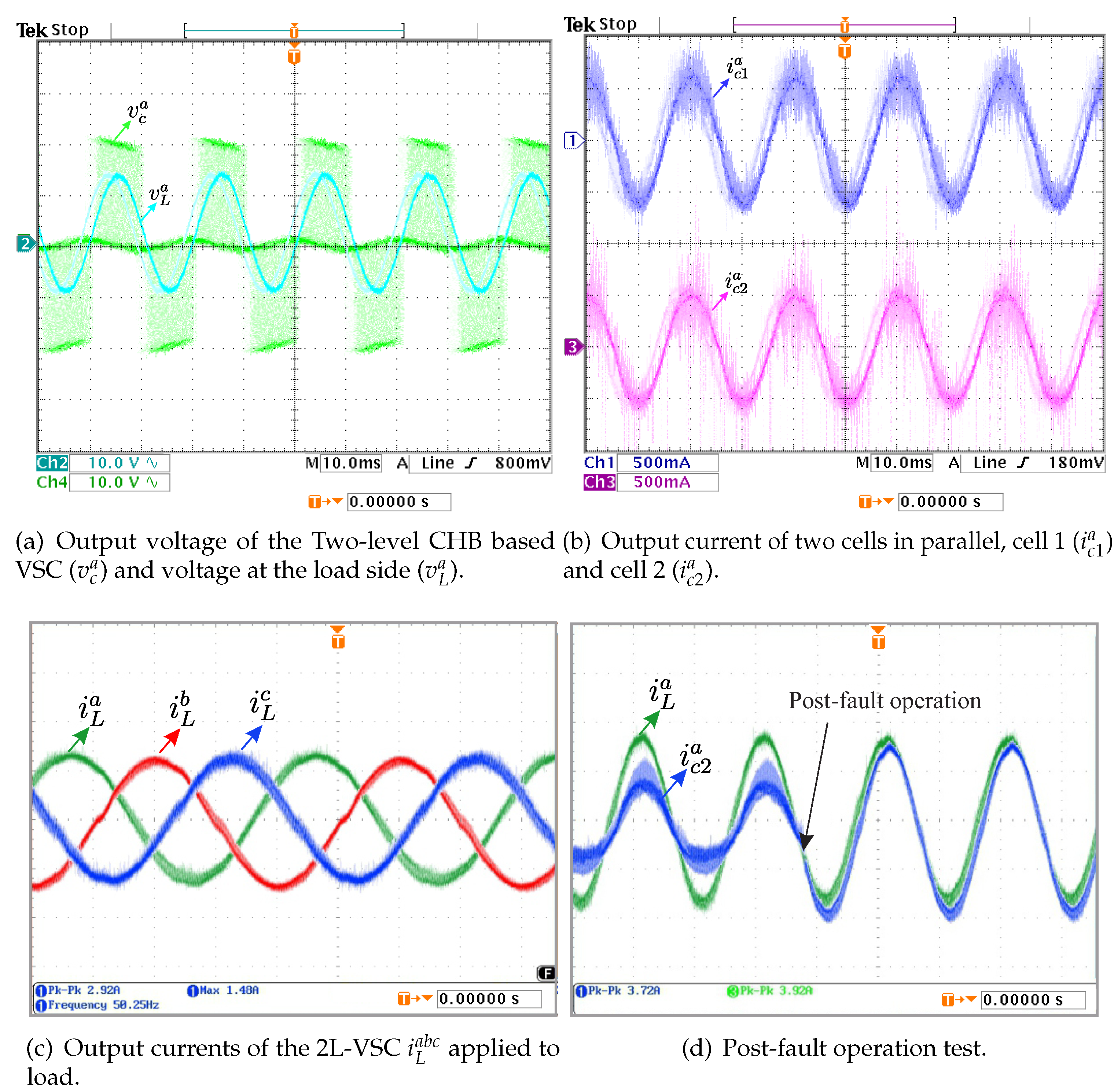
Figure 6 (a), the output voltage of the 2L-VSC can be observed before the output filter (
), where a switched waveform generated by the PWM modulation applied to the converter can be seen. After the output filter, a sinusoidal waveform without harmonics is observed because the output filter is configured as a low-pass filter, attenuating high-order harmonics. At the same time, the current distribution in two modules connected in parallel can be illustrated in
Figure 6 (b), where it can be concluded that the current distribution per module is practically equivalent.
On the other hand,
Figure 6 (c) depicts the voltages of the three phases measured at the point of common coupling (PCC) at the three-phase load side. The applied voltage to the load generates a symmetric current flow across the two parallel-connected cells (
and
), resulting in a quantified current of 3.72 A peak-to-peak on the load.
Figure 6 (d) illustrates how the current on the cell 2 (
) doubles to keep the current in the load (
) constant when the cell 1 is intentionally disconnected (
= 0A), emulating a post-fault behavior. These experimental results demonstrate the robustness of the proposed 2L-VSC with redundant cells operating in parallel making it particularly useful for those applications where high reliability is required.
4. Seven-level multi modular VSC topology
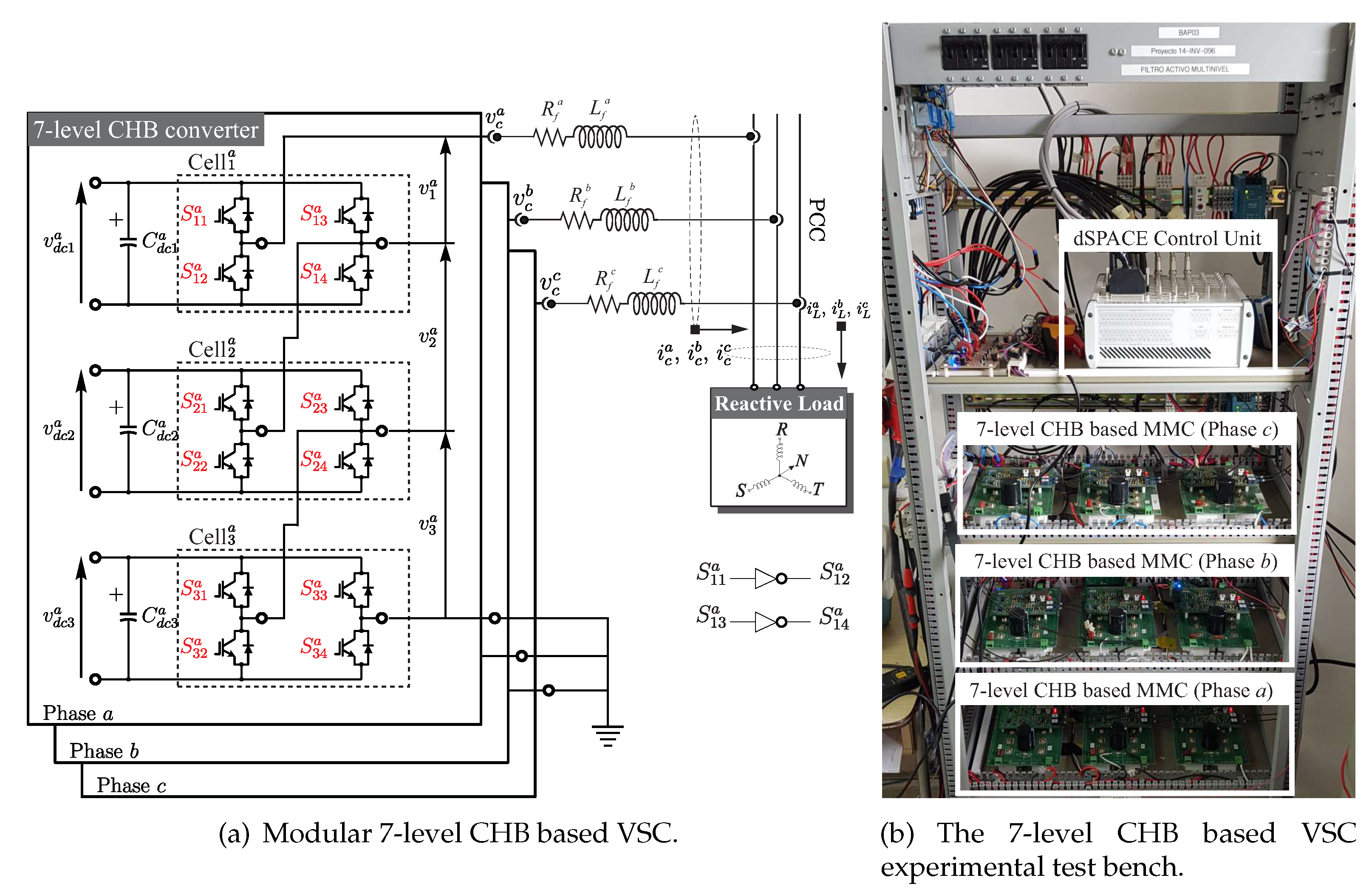
The scalable 7L-VSC topology, which is based on CHB cells, consists of a three independent cells per phase connected in series with independent DC-link (
), as depicted in
Figure 7 (a). This operational scheme incorporates SiC-MOSFET switching semiconductor devices and an output inductance
which operates as a filter at the output of the converter. The DC-link voltage (
) serves as the energy source, while the switching semiconductors synthesize the signals that are injected into the load at the connection point. The output inductance attenuates the harmonic effects resulting from the switching of the power devices in the converter.
Figure 7 (b) illustrates the integration of the different elements that comprise the experimental test bench of the 7L-VSC. One notable advantage of this design is its versatility and modularity, allowing for multiple configurations with minimal changes to the converter’s structure. Additionally, it is possible to expand the number of levels by adding more cascaded cells.
4.1. Seven-level multi modular VSC experimental results
The 7L-VSC tests are performed by interconnecting three cells in cascaded per phase. The
voltage feeding each cell are independently set to 30V, resulting in a total of 90V maximum output voltage for each phase of the seven-level converter. To verify the correct operation of the 7L-VSC, the converter output is connected through the output filter to a three phase resistive load (
= 16
). A switching frequency of 33kHz is configured.
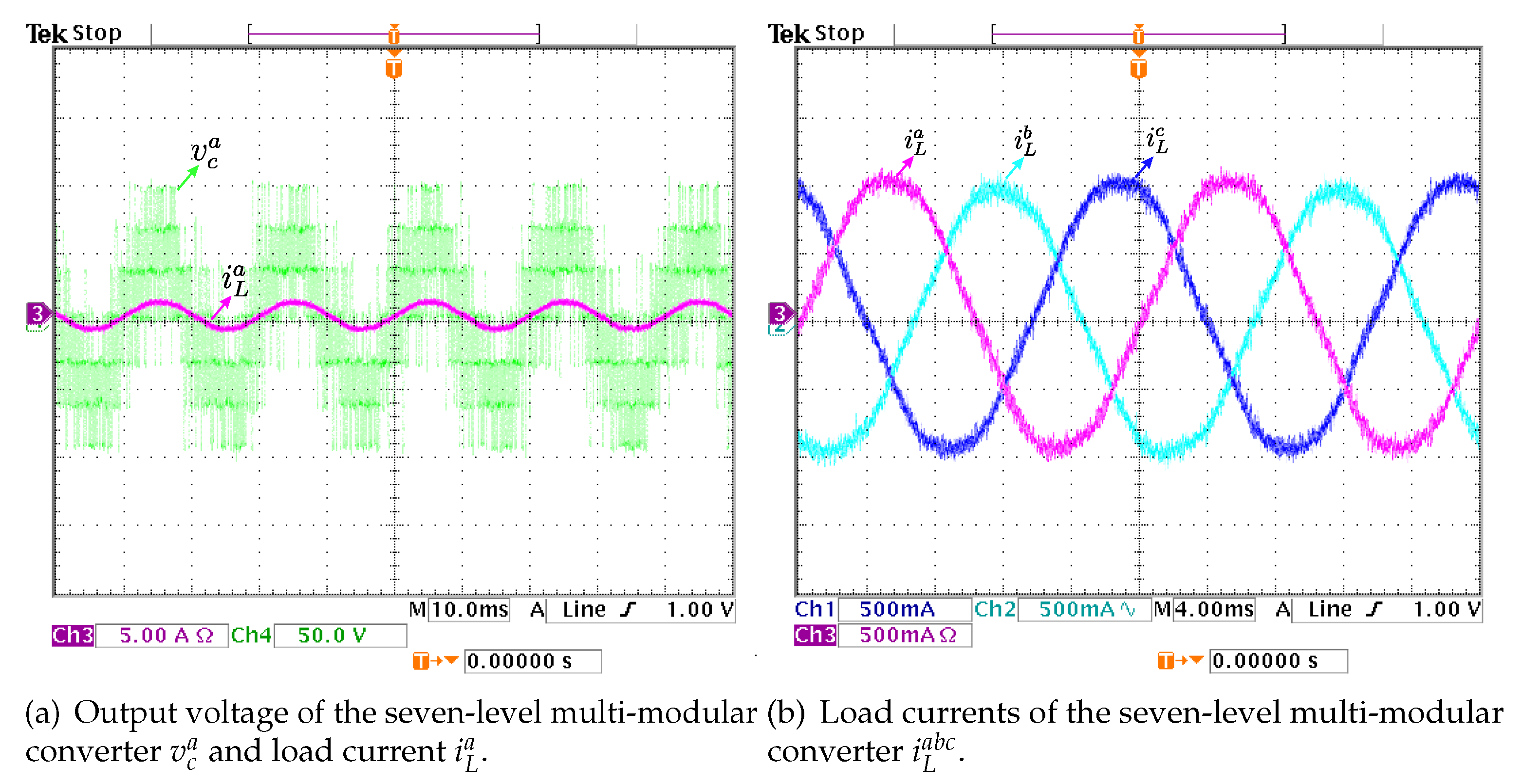
Figure 8 (a) shows the output voltage of one phase of the 7L-VSC before the output filter and the current
generated on the resistive load for phase "a". These graphs demonstrate that the current supplied to the load exhibits low harmonic distortion, which is expected due to the multi-level converter’s capability to generate sinusoidal signals.
Figure 8 (b) shows the Output currents of the seven-level multi-modular converter at the point of common coupling applied to three-phase load.
5. Voltage source matrix converter topology
The matrix converter (MC) is a single-stage AC-AC converter capable of directly supplying an "
n" phase load from an "
m" phase source (
MC) without the need for intermediate AC-DC conversion stages [
24]. The main advantages of MCs compared to widely used back-to-back conversion systems, which consist of rectifier stages connected to an inverter with an intermediate energy storage stage (capacitor bank), are as follows: reduced size, lightweight and long lifespan due to the absence of large electrolytic capacitors in the main circuit and high efficiency due to a single power conversion stage resulting in fewer switch losses compared to two-stage converters. Given these advantages, MCs are currently used in a wide range of AC-AC conversion applications, such as industrial applications requiring variable-speed electric motor drives, electric mobility, and more recently, wind energy conversion systems [
25,
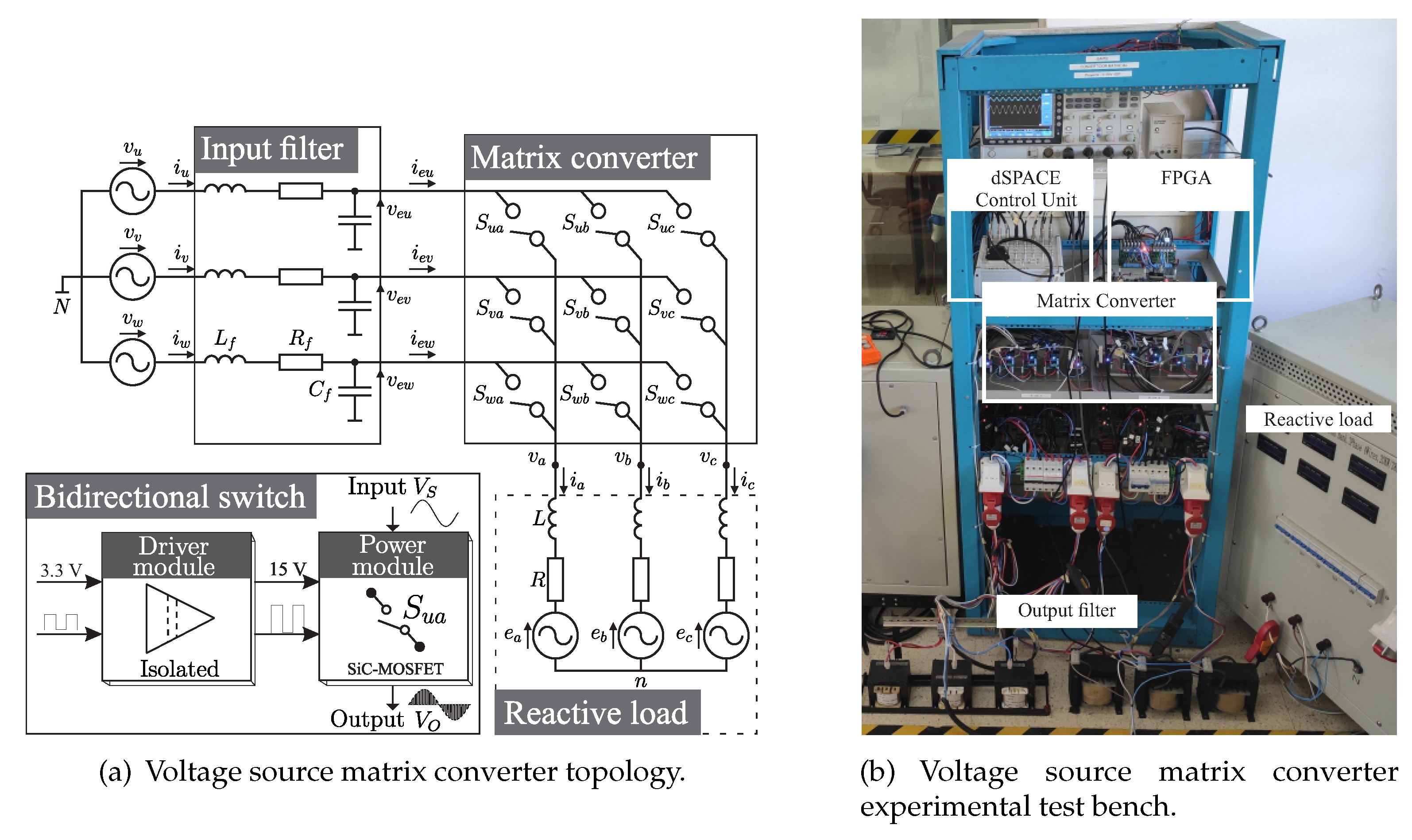
26]. The general topology for the MC is shown in
Figure 9 (a). In this case, a voltage-source matrix converter (VSMC) is obtained. To achieve good performance, the VSMC should be equipped with a source filter. The source filter is generally required to minimize high-frequency components in the input currents and reduce the impact of disturbances on the input grid. However, the size of the filter elements is inversely proportional to the VSMC’s switching frequency.
Figure 9 (b) shows the implemented experimental setup of the VSMC based on bidirectional switches designed using SiC-MOSFET semiconductor devices.
5.1. Bidirectional switch design
The bidirectional switch (Bi-Sw) design is divided into two main parts dominated control block and power block, respectively.
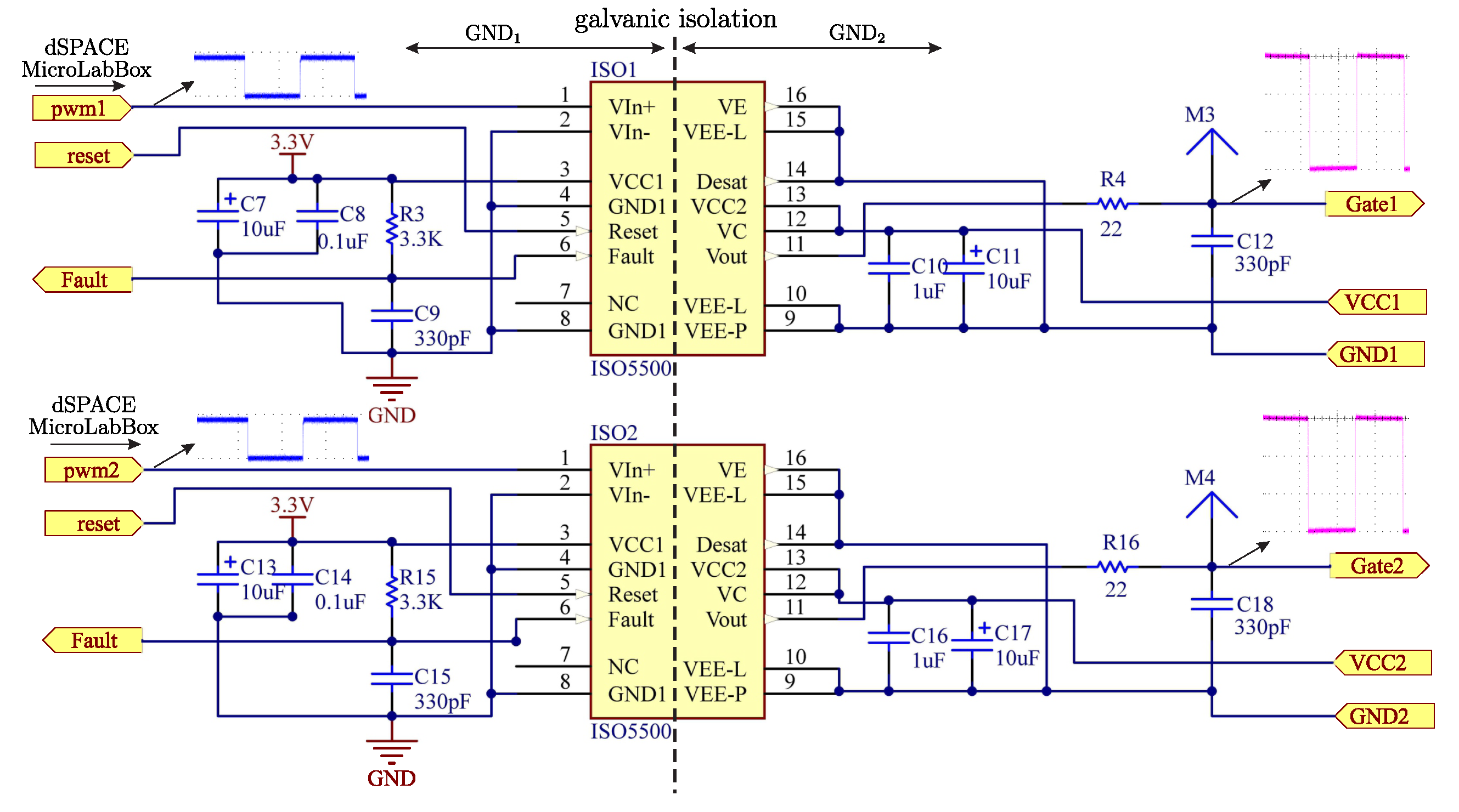
Figure 9 (a) shows the block diagram of the basic Bi-Sw operation. The control module performs signal conditioning for voltage and current levels (3.3V to 15V) required by the power module for proper operation of its components, and electrical noise isolation. The power module is based on the SiC-MOSFET semiconductor device, which basically works in cut-off and saturation zones at all times, controlling the current flow in both directions. The driver module has been implemented using the ISO5500 device. The ISO5500 is a gate driver device for IGBT and power MOSFET semiconductors, it has TTL input and a power output separated by a capacitive isolation barrier. This isolation barrier makes that there is a separation between the input signal grounds and the power stage, preventing voltage and current noise, produced by high switching and power can disturb the digital control devices. In
Figure 10, the electrical diagram of the driver module is observed, it consists of two main driver devices ISO5500, the first stage is powered with 3.3V and has the inputs PWM1 and PWM2, responsible for receiving the control signals from the MicroLabBox control unit. The second stage is fed with VCC1 = VCC2 = 15V, which corresponds to an output stage and higher power that is responsible for properly biasing the SiC-MOSFETs, Gate1 and Gate2 outputs, respectively.
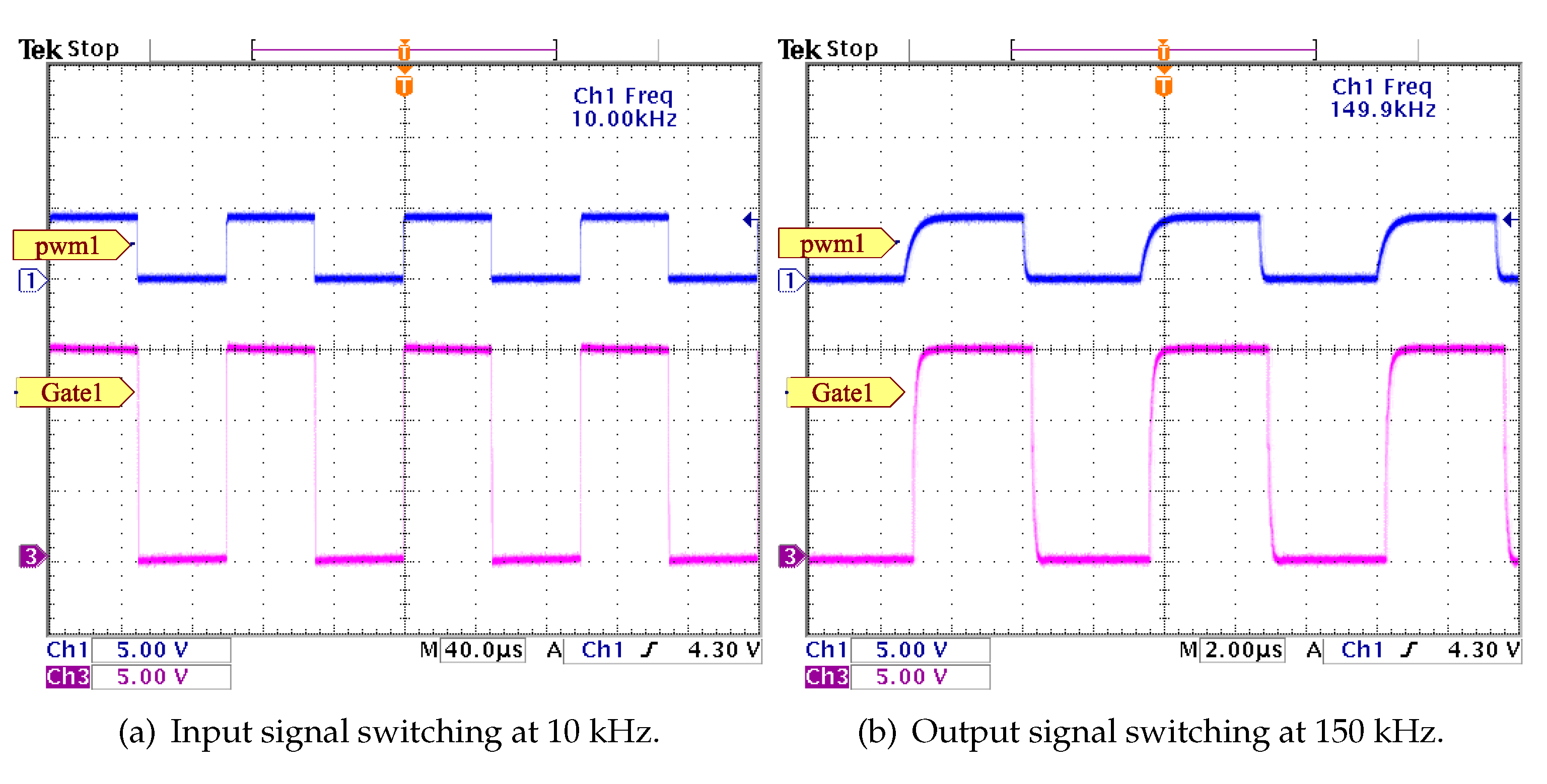
Figure 11 shows the evaluations of the module at different switching frequencies.
Figure 11 (a) corresponds to a PWM test signal equal to 5V/10kHz input PWM1 and the output response at Gate1 of 15V peak, measured by oscilloscope probes, is observed. A similar result is presented in
Figure 11 (b) for a signal equal to 5V/150kHz, where both experiments show very good responses to high switching frequencies.
The Bi-Sw power module is implemented with a set of SiC-MOSFETs (SCH2080KE) power semiconductor devices. The SCH2080KE packages have a built-in anti-parallel diode, which makes it possible for the current to have an alternative path when changing direction. This configuration of power semiconductors results in the formation of a switch capable of blocking voltages and currents in both directions with a wide bandwidth range.
5.2. Voltage source matrix converter experimental results
VSMC testing is performed using the experimental test bench described in the
Figure 9 (b), where an AC voltage variator is used as input source and at the output balanced three phase loads type
connected in star of values equal to
R = 16
and
L = 10 mH. For this test, the space vector modulation (SVM) strategy has been used, in which the 27 valid vectors of the MC are used to obtain a desired output voltage. For the implementation of the SVM it is necessary to measure the input voltages (
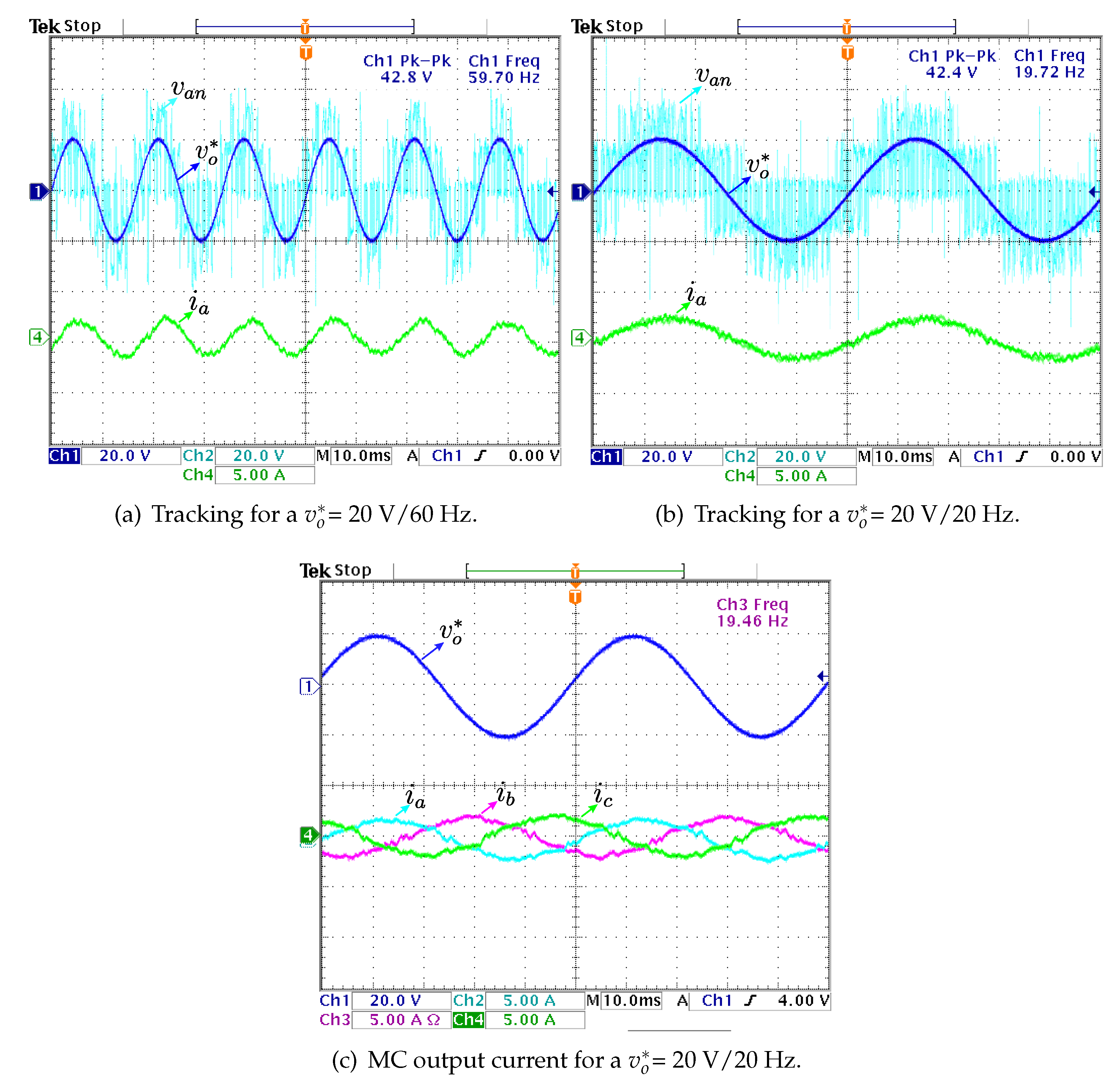
) to the VSMC. The results in
Figure 12 are obtained at a sampling frequency
. In
Figure 12 (a), the waveforms of the output voltage
and output current
are observed for a reference
= 20V/60Hz, and in
Figure 12 (b) the same test performed but for a frequency of
= 20V/20Hz. The waveforms of the three-phase output currents are shown in
Figure 12 (c). The results obtained show the correct tracking in the desired reference as well as the output currents on the
load present an expected sinusoidal shape.
6. Conclusion
In this article, we have presented a comprehensive approach to the design of VSCs, focusing on three types of converters based on SiC-MOSFET semiconductor devices. We have addressed the limitations of conventional AC-DC-AC 2L-VSCs and explored alternative solutions to improve overall performance and reliability. Our experimental results have shown the effectiveness of these VSC topologies in various operating conditions, including fault conditions. The parallel operation has provided valuable insights into the behavior and reliability of the converters, demonstrating their robustness and potential for practical applications in applications where a scalable power converter is required. On the other hand, the modular 7L-VSC based on CHB cells has demonstrated its capability to generate sinusoidal voltages and currents with low harmonic distortions at the load side. The modularity of the 7L-VSC based on CHB cells simplifies its extension to higher levels, making it a competitive choice in the new era of VSCs in applications where a power quality is required. Furthermore, experimental results shows that the VSMC has emerged as a promising solution for direct AC-AC power interfacing without the need for energy storage elements. The utilization of fully controlled bi-directional switches enables the generation of a three-phase sinusoidal voltage with adjustable amplitude and frequency. The incorporation of SiC-MOSFET semiconductor devices in these converters offers the advantage of higher switching frequencies, contributing to enhanced performance and reduced size compared to conventional converters.
Author Contributions
Conceptualization, R.G. and S.T.; methodology, R.G. and J.P. software, S.T. and E.M.; validation, R.G., J.P., S.T and E.M.; formal analysis, R.G., S.T, E.M. and J.P.; investigation, R.G., S.T., E.M. and J.P.; writing, original draft preparation, R.G. and S.T.; writing, review and editing, R.G. and S.T.; visualization, R.G. and S.T.; project administration, R.G.; funding acquisition, R.G.
Funding
This research has been funded through the Consejo Nacional de Ciencia y Tecnología (CONACYT)-Paraguay, Grant Number POSG16-05, Grant 14-INV-096, Grant 14-INV-097 and Grant PINV15-584.
Conflicts of Interest
The authors declare no conflict of interest.
Abbreviations
The following abbreviations are used in this manuscript:
| AC |
Alternating current |
| Bi-Sw |
Bidirectional switch |
| CHB |
Cascade H-Bridge |
| DC |
Direct current |
| IGBT |
Isolated Gate Bipolar Transistors |
| 2L-VSCs |
Two-level voltage source converters |
| 7L-VSCs |
Seven-level voltage source converters |
| MC |
Matrix converter |
| MMC |
Modular multilevel converter |
| MOSFET |
Metal-Oxide-Semiconductor Field-Effect Transistor |
| PWM |
Pulse-width modulation |
| PCC |
Point of common coupling |
|
Resistive and inductive load |
| SVM |
Space vector modulation |
| SiC |
Silicon Carbide |
| TTL |
Transistor-transistor logic |
| VSC |
Voltage source converter |
| VSMC |
Voltage source matrix converter |
| Nomenclature |
|
Dc-link capacitor |
|
, ,
|
Load phase currents |
|
, ,
|
Converter phase currents |
|
, ,
|
Converter phase voltages |
|
MC input voltage |
|
MC output phase voltage |
|
MC output current |
|
Sampling time |
|
Dc-link voltage |
|
Filter resistance |
|
Filter inductance |
References
- Murillo-Yarce, D.; Rivera, M.; Restrepo, C.; Rodríguez, R.; Wheeler, P.W.; Zanchetta, P.; Mirzaeva, G. Sequential Predictive Current Control of a VSI with Common-Mode Voltage Reduction. IEEE Proc. PEMD 2021. [Google Scholar]
- Milev, K.; Yaramasu, V.; Dekka, A.; Kouro, S. Predictive control of multichannel boost converter and VSI-based six-phase PMSG wind energy systems with fixed switching frequency. IEEE Proc. PEDSTC. IEEE, 2020, pp. 1–6.
- Abdelaziz, F.; Azzouz, Z.e.; Omari, A. Common mode voltage mitigation using a new modified model predictive control (mmpc) in a three phase voltage source inverter. Proc. ENERGYCon. IEEE, 2020, pp. 93–97.
- Gil-González, W.; Escobar-Mejía, A.; Montoya-Giraldo, O. Model Predictive Direct Power Control Applied to Grid-Connected Voltage Source Inverters. Proc. PEDG. IEEE, 2020, pp. 610–614.
- Xu, J.; Soeiro, T.B.; Gao, F.; Chen, L.; Tang, H.; Bauer, P.; Dragičević, T. Carrier-based modulated model predictive control strategy for three-phase two-level VSIs. Trans. Energy Conver. 2021, 36, 1673–1687. [Google Scholar] [CrossRef]
- Rojas, D.; Rivera, M.; Toledo, S.; Wheeler, P. Predictive control techniques applied to a 2L-VSI. Proc. CHILECON. IEEE, 2021, pp. 1–6.
- Rojas, D.; Rivera, M.; Muñoz, J.; Wheeler, P. Cascaded predictive control for a three-phase VSI with different cost functions. Proc. CHILECON. IEEE, 2021, pp. 1–6.
- Xu, J.; Gao, F.; Soeiro, T.B.; Chen, L.; Tarisciotti, L.; Tang, H.; Bauer, P. Model Predictive Control for the Reduction of DC-link Current Ripple in Two-level Three-phase Voltage Source Inverters. Proc. ECCE. IEEE, 2020, pp. P–1.
- Dabkara, M.; Gupta, Y.; Sharma, N.; Sharma, A. A Solar PV Standalone System with Predictive Current Controlled Voltage Source Inverter. Proc. ICETCE. IEEE, 2020, pp. 1–6.
- Comparatore, L.; Renault, A.; Pacher, J.; Rodas, J.; Gregor, R. Finite Control Set Model Predictive Control Strategies for a Three-Phase Seven-level Cascade H-Bridge DSTATCOM. IEEE Proc. ICRERA, 2018, pp. 779–784.
- Xu, Z.; Liu, Y.; Cao, B.; Liu, B.; Li, S. Research and Application of Compensation Characteristics of DSTATCOM under Unbalanced Load. IEEE Proc. IAEAC, 2018, pp. 806–810.
- Renault, A.; Rodas, J.; Comparatore, L.; Pacher, J.; Gregor, R. Modulated Predictive Current Control Technique for a Three-Phase Four-Wire Active Power Filter based on H-bridge Two-Level Converter. IEEE Proc. UPEC, 2018, pp. 1–6.
- Kehl, Z.; Glasberger, T.; Peroutka, Z. Finite Control Set Model Predictive Control of Static Compensator. IEEE Proc. ISIE, 2019, pp. 858–863.
- Praženica, M.; Resutík, P.; Kaščák, S. Practical Implementation of the Indirect Control to the Direct 3 x 5 Matrix Converter Using DSP and Low-Cost FPGA. Sensors 2023, 23. [Google Scholar] [CrossRef] [PubMed]
- Renault, A.; Ayala, M.; Comparatore, L.; Pacher, J.; Gregor, R. Comparative Study of Predictive-Fixed Switching Techniques for a Cascaded H-Bridge Two level STATCOM. IEEE Proc. UPEC, 2018, pp. 1–6.
- Maqueda, E.; Toledo, S.; Gregor, R.; Caballero, D.; Gavilán, F.; Rodas, J.; Rivera, M.; Wheeler, P. An assessment of predictive current control applied to the direct matrix converter based on SiC-MOSFET bidirectional switches. 2017 IEEE Southern Power Electronics Conference (SPEC), 2017, pp. 1–6. [CrossRef]
- Pacher, J.; Rodas, J.; Gregor, R.; Rivera, M.; Renault, A.; Comparatore, L. Efficiency analysis of a modular H-bridge based on SiC MOSFET. Taylor & Francis Trans. 2019, 7, 59–67. [Google Scholar]
- Ipoum-Ngome, P.G.; Mon-Nzongo, D.L.; Flesch, R.C.C.; Song-Manguelle, J.; Wang, M.; Jin, T. Model-free predictive current control for multilevel voltage source inverters. Trans. Ind. Electron. 2020, 68, 9984–9997. [Google Scholar] [CrossRef]
- Vu, H.C.; Lee, H.H. Model-Predictive Current Control Scheme for Seven-Phase Voltage-Source Inverter With Reduced Common-Mode Voltage and Current Harmonics. IEEE J. Emerg. Sel. Top. Power Electron. 2020, 9, 3610–3621. [Google Scholar] [CrossRef]
- Zhang, L.; Yuan, X.; Wu, X.; Shi, C.; Zhang, J.; Zhang, Y. Performance evaluation of high-power SiC MOSFET modules in comparison to Si IGBT modules. IEEE Transactions on Power Electronics 2019, 34, 1181–1196. [Google Scholar] [CrossRef]
- Jiao, N.; Wang, S.; Liu, T.; Wang, Y.; Chen, Z. Harmonic Quantitative Analysis for Dead-Time Effects in SPWM Inverters. IEEE Access 2019, 7, 43143–43152. [Google Scholar] [CrossRef]
- Li, B.; Xu, J.; Ye, J.; Wang, H.; Huang, S.; Li, Y.; Shen, A. A New Model-Based Dead-Time Compensation Strategy for Cascaded H-Bridge Converters. IEEE Transactions on Industrial Electronics 2023, 70, 3793–3802. [Google Scholar] [CrossRef]
- Infineon-Semiconductors. 600 V High and Low Side Driver IC, 2017.
- Gili, L.C.; Dias, J.C.; Lazzarin, T.B. Review, Challenges and Potential of AC/AC Matrix Converters CMC, MMMC, and M3C. Energies 2022, 15. [Google Scholar] [CrossRef]
- Toledo, S.; Caballero, D.; Maqueda, E.; Cáceres, J.J.; Rivera, M.; Gregor, R.; Wheeler, P. Predictive Control Applied to Matrix Converters: A Systematic Literature Review. Energies 2022, 15. [Google Scholar] [CrossRef]
- Diaz, M.; Cárdenas Dobson, R.; Ibaceta, E.; Mora, A.; Urrutia, M.; Espinoza, M.; Rojas, F.; Wheeler, P. An Overview of Applications of the Modular Multilevel Matrix Converter. Energies 2020, 13. [Google Scholar] [CrossRef]
|
Disclaimer/Publisher’s Note: The statements, opinions and data contained in all publications are solely those of the individual author(s) and contributor(s) and not of MDPI and/or the editor(s). MDPI and/or the editor(s) disclaim responsibility for any injury to people or property resulting from any ideas, methods, instructions or products referred to in the content. |
© 2023 by the authors. Licensee MDPI, Basel, Switzerland. This article is an open access article distributed under the terms and conditions of the Creative Commons Attribution (CC BY) license (http://creativecommons.org/licenses/by/4.0/).
