1. Introduction
With the increasing popularity of consumer electronics products, such as laptops, smartphones, display cards, and tablets, high-quality Printed Circuit Board (PCB) manufacturing is important. Because of this surge in the demand for PCBs in the market, manufacturers are required to produce PCBs in large quantities. However, maintaining the quality of such large numbers of PCBs is challenging. With the advent of computer vision [
1] and artificial intelligence [
2] techniques, automated computer visual inspection methods are found to be beneficial for improving the performance for high volume industrial production.
One typical approach for automated computer visual inspection is based on template-matching method [
3,
4,
5] with a flaw-free reference. Basic template-based approaches accomplish defect detection by measuring the similarity (or dissimilarity) between the given test image and the reference. A common drawback of some template matching approaches is that proper alignment between the test image and template is desired for the correlation computation. However, for many applications, the enforcement of alignment operations may be difficult, resulting in degradation in detection accuracy. Furthermore, some of these technique focus only on the inspection of solder joints or bare PCBs without components. Nevertheless, component placement inspection is a significant and challenging problem for PCB manufacturing. Many defects are caused by errors in PCB component placement, such as missing or misaligned components, or the incorrect rotation of the components.
Automated component placement inspection on a PCB can be achieved by the employment of sematic segmentation or object detection methods. The sematic segmentation techniques [
6,
7] aim to separate images under examination into regions. Each individual region belongs to an independent component on PCB [
8,
9]. One challenging issue for the segmentation-based is the dense and/or uneven distributions of components on a board. It may be difficult to detect a component in a densely populated region on the PCB [
8,
9]. In addition, large varieties of components may further degrade the accuracy for component detection. For the components with small sizes, lower segmentation accuracy may be introduced due to the class-imbalanced problem [
10,
11]. Therefore, it would be difficult to adopt the segmentation-based surface defect detection techniques [
12] for the component placement inspection.
The region-based Convolutional Neural Networks (CNNs) [
13,
14,
15,
16] for object detection have also been found to be effective. Many of the techniques attains high detection accuracy by the employment of anchor boxes as detection candidates [
17,
18,
19]. Anchor boxes are the boxes with various sizes and aspect ratios. A large set of anchor boxes [
11] may be required for accurate detection. Subsequently, high computation overhead is usually introduced for both training and inference. In addition, expensive manual labeling efforts are required when the varieties of components are high [
20].
Alternatives to the anchor based approaches are to represent each object as a single [
21] or multiple keypoints [
22,
23]. For the technique with a single keypoint, the keypoint of an object is the center of the bounding box of the object. When an object is represented by a pair or a triplet of keypoints, each keypoint represents the center or corners of the bounding box. The corresponding object detection operations are equivalent to finding the keypoints of the objects. The need for anchor boxes is then bypassed.
Although the keypoint-based methods have the advantages of simplicity and high detection accuracy, the reusability of network models are not taken into consideration. As a result of supply chain management for components, even for the same products, it is likely that the corresponding PCBs are constantly updated by the accommodation of new component classes and removal of old ones. When the Neural Network (NN) models are shared by all the classes, it would then be necessary to re-train the networks for the updated PCBs. For the component classes which are shared by original and updated PCBs, the variations in detection accuracy would be likely due to the re-training. Therefore, robustness in inspection accuracy would be an important issue. Although the reusability and robustness can be improved by training a dedicated NN for each component class, the number of NNs will grow. As a result, similar to anchor-based approaches, high computational complexities for both training and inference may be necessary for the keypoint-based methods for the component detection.
The objective of this study is to develop a novel automated computer vision algorithm for component placement inspection on PCBs. The corresponding Internet of Things (IoT) systems will also be built for field test. The proposed algorithm is a keypoint based technique. Therefore, it has simple training and inference process without the requirement of anchor boxes. The efforts for manual labelling can be significantly lowered. In addition, no templates are necessary. The alignment issues for the template-based techniques can then be avoided. In the proposed algorithm, the inspection for components from the same class is regarded as a single task. In the architecture, the tasks are separated into more than one groups. Different tasks in the same group may share the same network layers for feature extraction. Each task only has its own dedicated output layers. The network size and computational complexities for the algorithm may still remain low even for a PCB consisting of large number of component classes.
To alleviate the efforts for re-training when PCBs are updated and/or new PCB target are available, the reuse of NNs of existing components are also taken into consideration for our training operations. When a new component class is accommodated, training is necessary only for the network layers for the new class, and for the classes sharing the same group with the new class. For the classes belonging to other groups, the corresponding layers can be directly reused. In this way, the training efforts for the inclusion of new classes can be lowered.
The remaining parts of the this study is organized as follows. In
Section 2, we present the proposed algorithm for component placement inspection in detail.
Section 3 contains some experimental results for the algorithm. The concluding remarks are then included in
Section 4.
2. Proposed Algorithm
In this section, we start with the keypoint-based NN for the component placement inspection with single class. The keypoint-based NN is then generalized to multiple classes with model reuse. The two-stage training procedure for the model reuse is then presented in detail. A list of commonly used symbols is shown in
Table A1.
2.1. Component Placement Inspection for a Single Class
Figure 1 shows the block diagram of proposed NN model for the single-class component detection. As shown in the figure, the network model can be separated into two portions: frontend network and backend network. The frontend network is used for the feature extraction of the input image. The backend network produces the results for component placement inspection. It provides the heatmap indicating the likelihood of each pixel in the image belongs to the component. The size of the component can also be predicted by the backend network.
Let
X be an input image of width
W and height
H. Our goal is to produce a heatmap
Y with width
and height
, where
R is the output stride size. Let
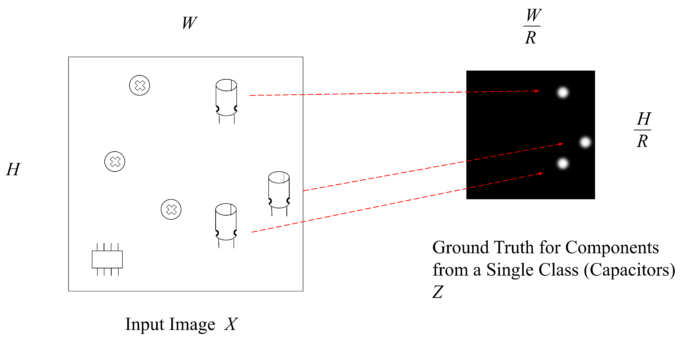
Z be the ground truth of
Y. The ground truth is determined by the keypoint of each component on the input image. As shown in
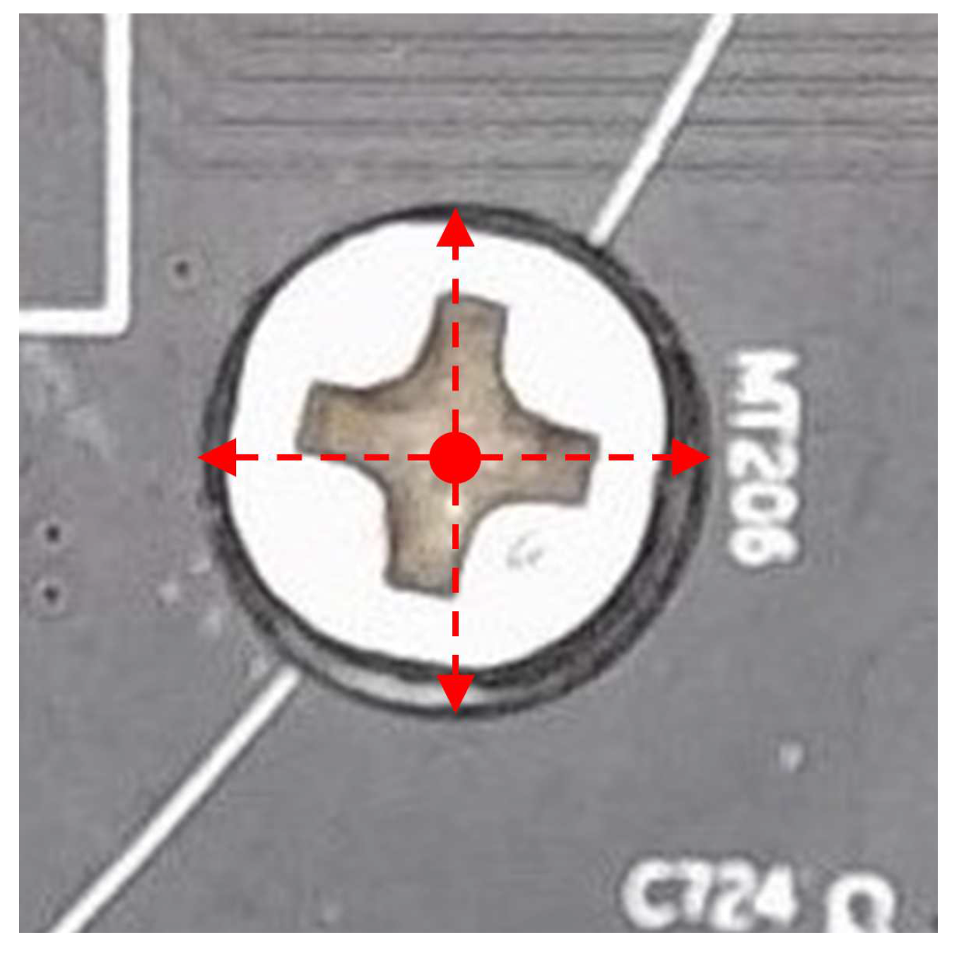
Figure 2, the keypoint of a component is the centroid of the component. For the sake of simplicity, assume that we only focus on the detection of components from a single class in the input image. Let
be the location of a component from the class. We then compute
Z for the component by splatting the keypoint of the component using Gaussian kernel. That is,
where
is the
-th pixel of the ground truth image
Z , and the
is the standard deviation dependent on the size of the component. In the case two or more components of the class are presented, the overlapping of the corresponding kernels are likely. We then take the element-wise maximum over the Gaussian kernels for components.
Figure 3 shows an example of ground truth image for the detection of capacitors on the PCB.
Let
be the loss function for heatmap the training of the proposed network model. A variant of focal loss function [
11] is adopted for the function
. That is,
where
where
is the
-th component of heatmap
Y, and the parameters
and
should be pre-specified before the training.
In addition to the detection of component location by heatmap
Y, it may be desired to find the component size for inspection. This can be accomplished by appending a network branch in the backend network, as shown in
Figure 1. Let
be the output of the branch for size estimation, where
and
are the images with width
and height
. Furthermore, let
K be the number components, and
,
be the ground truth of width and height of the
k-th component,
. The loss function for the component sizes is defined as
where
and
are the estimated width and height of component
k from
S. Let
be the ground truth location of the keypoint of the
k-th component,
. The estimation
and
can be computed by
The total loss for the training of the proposed network model, denoted by
, for single class is then given by
2.2. Component Placement Inspection for Multiple Classes
As shown in
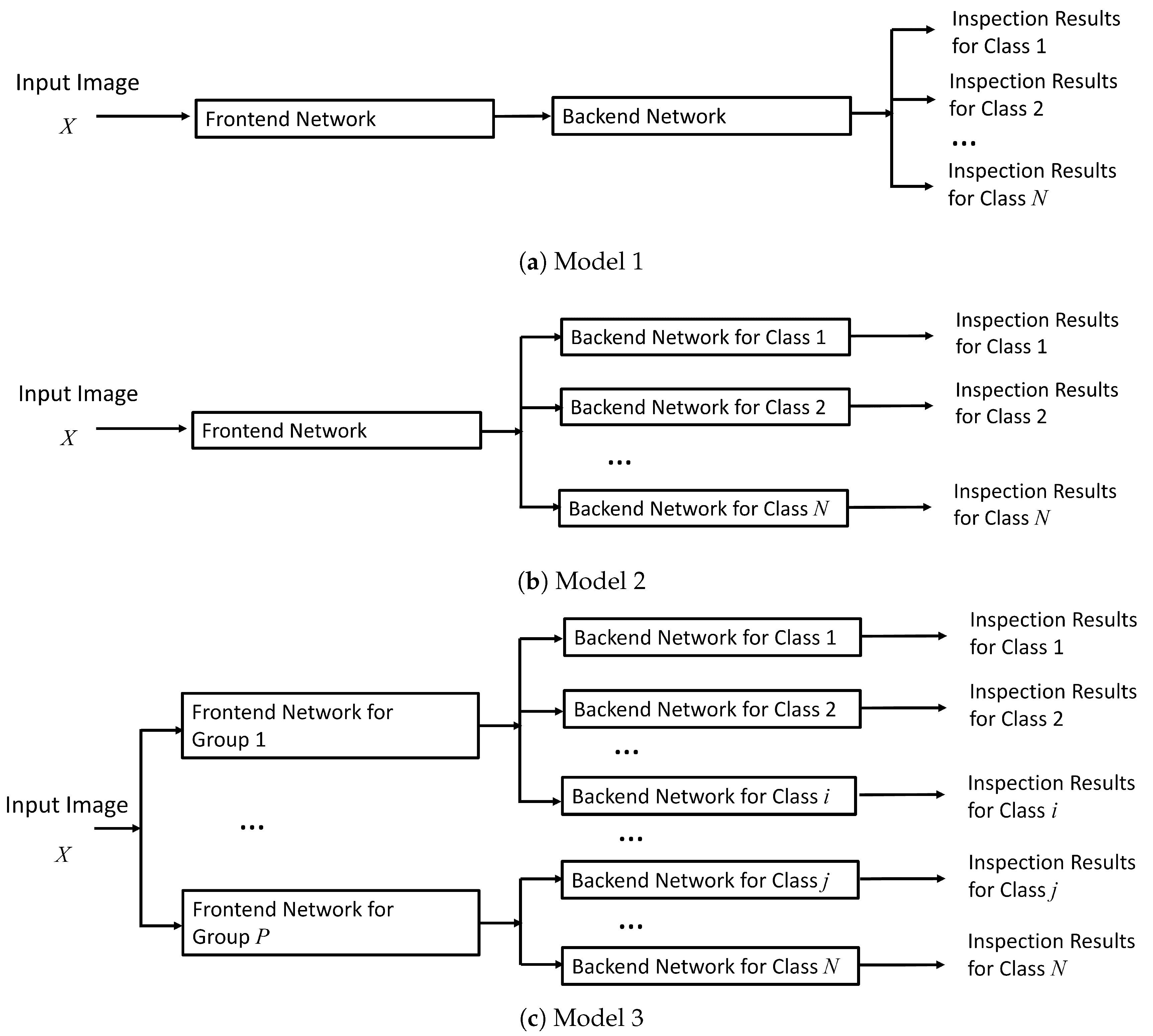
Figure 4, the NN model for the component placement inspection for multiple classes can be viewed as an extension of its counterpart for single class. Let
N be the number of component classes for the inspection. Consequently, there are
N heatmaps for the detection of components, where the
c-th heatmap
Y is adopted for the detection of components in
c-th class. Likewise, there are
N pairs of images for the estimation of component sizes, where the
c-th pair
is used for the estimation of component sizes.
From
Figure 4, we can see that there are three network models for multiple classes. For the first approach, as shown in
Figure 4a, is a direct employment of the model for a single class for multiple classes. That is, all the classes share the same frontend network and backend network. When the number of component classes
N increases, the model size and computation latency for inference can be maintained. However, the shared frontend network and/or backend network may not be matched to a particular class. Therefore, the detection accuracy for the class may be degraded. Furthermore, the reusability of the model may be in important issue. Because all the classes in the model are jointly trained, the incorporation of new classes may result in the re-training of all the classes. Large overhead may then be required for the inspection of new PCBs, where the accommodation of new classes for component inspection is necessary.
The second model allows all the classes share the same frontend network for feature extraction. Furthermore, each class has its own dedicated output branches in the backend network, as shown in
Figure 4b. Because of the sharing of the frontend network, the overall model size and computation complexities can still be low for large number of classes
N. In addition, because there is a dedicated backend network for each class in the second model, it may outperform the first model for component inspection. Nevertheless, when the incorporation of new classes is desired, it may still be necessary to re-train all the existing classes because the shared frontend network needs to be fine tuned for the new class as well as the existing classes.
The third model can be viewed as an extension of the second model. We separate
N classes of components into
P groups in the third model. The classes belonging to the same group share the same frontend network for feature extraction. Therefore, there are
P frontend networks in the third model, as shown in
Figure 4c. One simple approach for carrying out the grouping is based on the shapes of the components. For example, components with similar shapes can be grouped together. The shape information for each group can then be fully exploited for producing accurate heatmaps for component placement prediction. Because there is a dedicated frontend network for each group for feature extraction, the third model may have superior performance over the first and the second model for component inspection. Moreover, the networks in the third model could be re-used. That is, the accommodation of a new component class may require the training of only the NNs in the group the new class belongs to. The networks in the other groups can be effectively re-used.
2.3. Two-Stage Training Process
The proposed two-stage training process can be applied for the three models proposed in
Section 2.2. There are two stages for the training of the models. The training operations at the first stage can be viewed as the pre-training operations for the frontend networks. Based on the results from the first stage, the goal at the second stage is for the refinement for the frontend networks and the complete training for the backend networks. The two-stage training operations is based on the training set with
a training images, denoted by
.
2.3.1. First Stage Training
The goal for training at the first stage for each network model is to provide an effective frontend network for feature extraction. This training process can be viewed as a representation learning process [
24] to fully exploit the features for subsequent generation of heatmaps for the backend networks. For each training image in
, data augmentation operations are employed to produce
b images. The employment of data augmentation is able to include more variations for the training set. Let
be the set of augmented images derived from the
i-th image in
. For a fixed
i, it is desired that the frontend network will produce similar features for the augmented images from the set of augmented images
. Conversely, images from different augmented sets should produce different features. For the PCB inspection, it is usually desired that the impacts on illumination to the inspection accuracy can be minimized. Therefore, the data augmentation in this study is to provide images with different illuminations. In this way, the proposed frontend networks for are less sensitive to the variations in illuminations on the PCBs.
The training at the first stage is carried out on tuple-by-tuple basis. For each training image
, a number of tuples are formed, where each tuple contains
elements. Let
be a tuple for
, where
is an image drawn randomly from the set
. Let
be the set of tuples from training image
. The loss function for the training at the first stage is given as
where the function
F denotes the frontend network.
2.3.2. Second Stage Training
At the second stage, both the frontend and the backend networks are trained by the training set
. The frontend networks acquired from the first stage are served as the initial frontend networks at the second stage. The initial backend networks are randomly generated. The loss function in (
6) is also adopted for the training at the second stage. That is,
where
and
are the
and
defined in (
2) and (
4) for the components in class
c, respectively.
An advantage of the two-stage training process is that the impact of illuminations for placement inspection can be effectively lowered. Based on the representation learning scheme at the first stage, features robust to illuminations can be provided for the subsequent heatmap generation. This is beneficial for attaining high accuracy for detecting components on PCB boards without introducing false alarms.
2.4. Examples of Frontend and Backend Networks
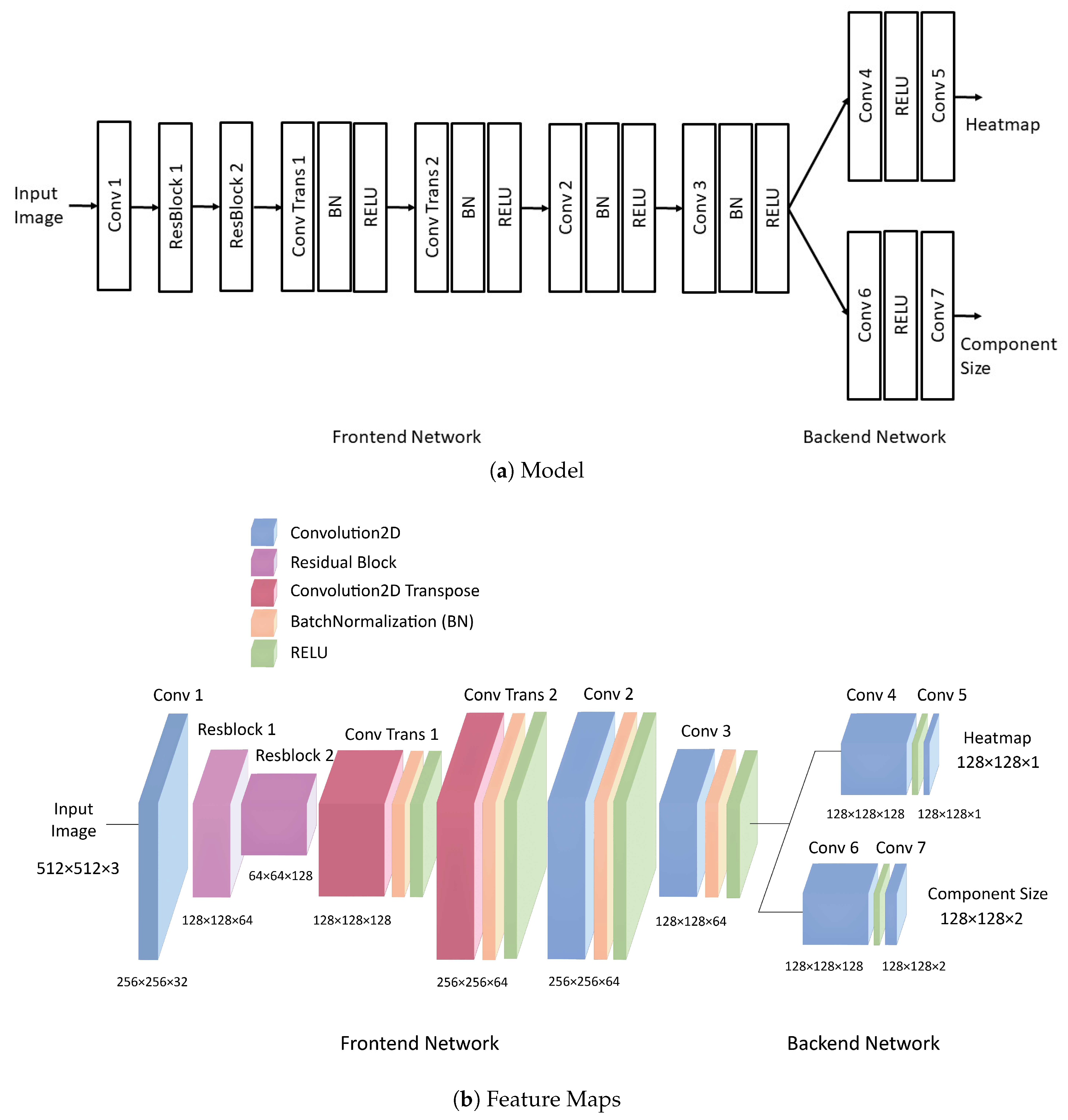
The frontend and backend networks considered in this study are not restricted to any specific types of networks. However, for the evaluation purpose, examples of frontend and backend networks are provided, as shown in
Figure 5, where the block diagram of the model and the feature maps produced by each layer of the model are revealed in
Figure 5a,b, respectively.
We can see from
Figure 5 that the complexities for the frontend network are higher than those for the backend network. In the frontend network, the Residual Blocks (ResBlock) [
25] and up-down networks [
26] are employed for compact and efficient feature representation. Each ResBlock contains a shortcut [
25] for efficient weight updating. The 2-dimenional Convolution (Conv) networks, together with their transposed (Conv Trans) counterparts, are adopted for the implementation of up-down networks. Both the Batch Normalization (BN) and REctified Linear Unit (RELU) activation functions are also included in residual blocks and up-down networks.
Each backend network is dedicated to only a single class. To reduce the complexities for the entire component inspection networks, each backend network has a simple architecture. We can observe from
Figure 5 that there are only two convolution layers for each backend network. The simplicity of backend networks is beneficial for facilitating both the training and inference operations especially when the number of classes
N is large for component inspection.
3. Experimental Results
This section provides the experimental results of the proposed work. The experimental setup is first presented. The performance metrics are then discussed. This is followed by numerical results and comparisons among the proposed and existing techniques.
3.1. Experimental setup
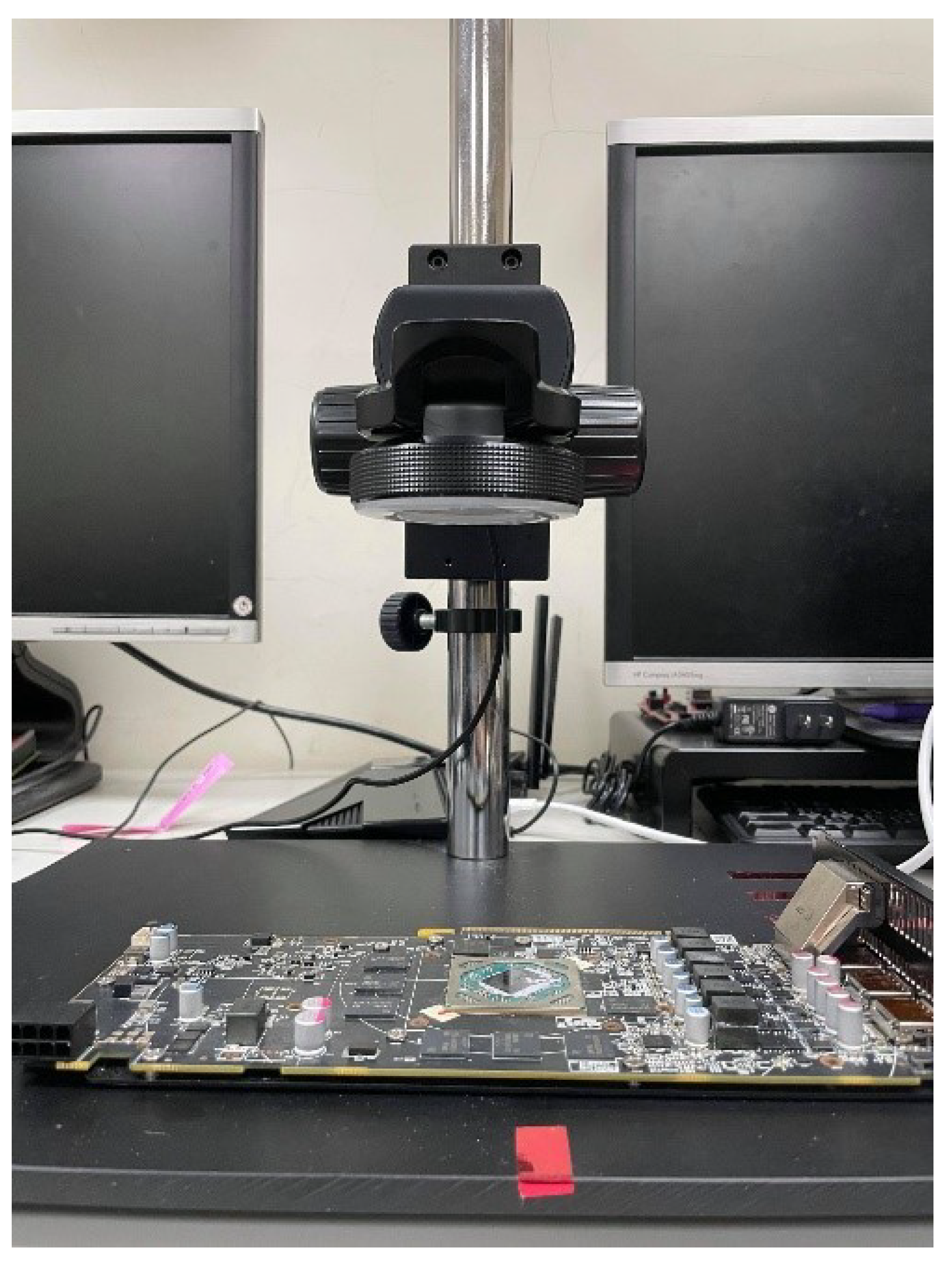
The setup of the experiments is shown in
Figure 6, which is a simple inspection platform with a high resolution industrial camera FLIR Blackfly S USB 3. The platform can be easily integrated into a real production line for online inspection. The development of NN models is based on Keras built on the top of Tensorflow 2.0.
In the experiment results, we consider only the inspection of components of screws, capacitors, mounting holes, 3-pin chips and 8-pin chips of the PCB, as shown in
Figure 7. That is, there are
component classes. In many assembly lines, some of these components such as screws may be placed on the PCB manually. As a result, component misplacements are likely. Furthermore, it may be difficult to perform accurate component inspection for components such as 3-pin chips because of the complex background, and the small component sizes. Successful inspection of the components shown in
Figure 7 would be a promising indication for accurate inspection of the other PCB components.
The images for our experiments have equal size
. That is, the height and width of input images are
. However, the sizes of different PCBs may vary. Therefore, when their sizes are larger, they will be divided into
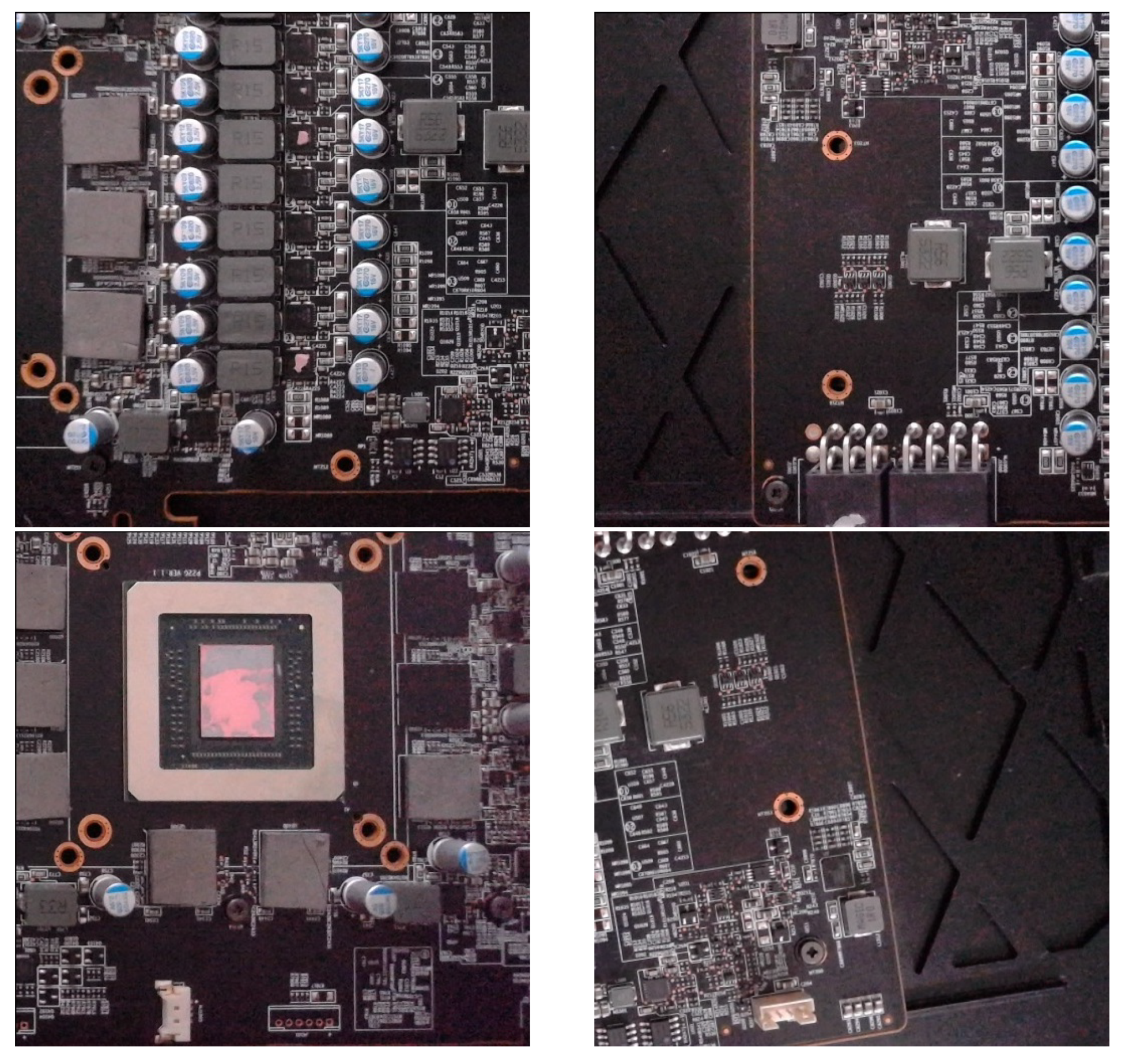
subimages for the inspection. To increase the varieties of training set, different cropping results from the training PCBs are adopted as training images. Some examples are shown in
Figure 8. The training set
contains
images. The
i-th image in the training set
is further augmented to from the set
containing
images. After different cropping and augmentation of images, 2880 images (e.g,
) with
are created for the training of the proposed NN model.
Table 1 shows the parameters at each layer of the basic NN model considered in this study. For the sake of simplicity, this model contains only one frontend network and one backend network for a single class inspection, where the names of layers are defined in
Figure 5. More frontend networks and/or backend networks with the same specification can be appended in the model for the applications requiring multiple groups with multiple classes.
Table 2 shows the specification of Model 1, Model 2 and Model 3 for five component classes. For meaningful comparisons, as shown in
Table 2, all the models have the same dimension
for input image
X. That is, original width and height are
. In addition, they have the same dimension
for output images
Y and
S. Because
, we see that the output stride size is
for heatmap generation.
We can also observe from
Table 2 that Model 1 has smallest size as compared with Model 2 and Model 3. This is because Model 1 has only a single frontend NN and a single backend NN shared by all the component classes. By contrast, in Model 2, a dedicated backend NN is assigned to each component class. Furthermore, all the component classes are separated into
grounps in the Model 3. In fact, the screws, mounting holes, and capacitors form the first group, and the 3-pin and 8-pin chips are in the second group. In Model 3, each group has its own fronend NN. The Model 3 therefore has largest size.
3.2. Performance metrics
The performance metrics considered in this study include the quality of component placement inspection, network size, and the computation time of the proposed model. The component inspection accuracy, such as Average Precision (AP) [
27,
28] value and F1 score [
27,
28], are used as the quality of component placement inspection in experiments. Images of PCBs not belonging to training set are adopted as the test set for the evaluation of AP value and F1 score. The network size is defined as the number of weights in the network. The network size indicates the memory resources required for the deployment of the network. The computation time is the inference latency for the model. It reveals the promptness of the model for inspection.
Both the AP value and F1 score are evaluated by precision and recall rates. For a given component class
c, let TP (True Positive) and FN (False Negative) be the number of components of class
c in the test set which are detected and missed, respectively. Let FP (False Positive) be the number of components from other classes in the test set which are falsely identified as components of class
c. The precision and recall [
27] rates are then defined as
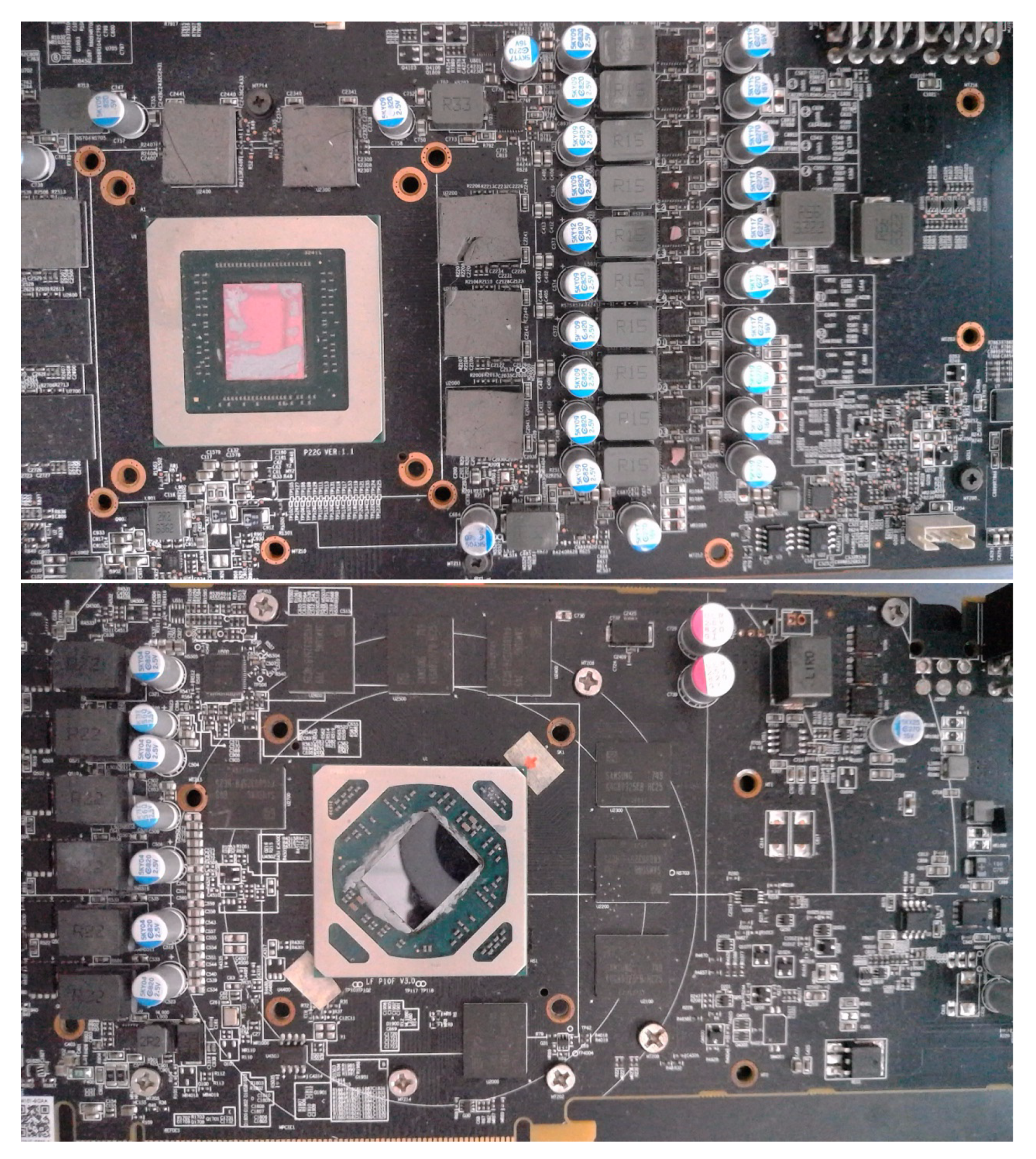
The measurements of precision and recall rates are based on the testing images extracted from the PCBs shown in
Figure 9, which are different from the training images.
Because different threshold values for detection may result in different pairs of precision and recall rates, a Precision-Recall curve could be obtained by sweeping the threshold values. The AP value is then defined as the area under the Precision-Recall curve. Higher AP values imply better Precision-Recall performance.
Given a pair of precision and recall rates, the computation of the corresponding F1 score [
27] is given by
The score provides a comprehensive evaluation based on Precision and Recall. Given a Precision-Recall Curve, the corresponding F1 score is obtained by finding the pair of precision and recall values on the curve attaining the maximum F1 score.
3.3. Numerical Results and Comparisons
Table 3 shows the corresponding AP values and F1 scores of the proposed two-stage training process for Model 1 for different components considered in this study. For comparison purpose, the AP values and F1 scores with only single-stage training process for Model 1 are also included, where the representation learning for the frontend network is omitted. The Model 1 by single-stage training can be viewed as the basic key-point algorithm [
21] for object detection. From
Table 3, it can be observed that two-stage training process is able to achieve higher AP values and F1 scores as compared with its single-stage counterpart. This is because the representation learning operations are beneficial for providing robust features for the subsequent heatmap generation and component size estimations.
The comparisons on AP values and F1 scores among Model 1, Model 2 and Model 3 are included in
Table 4. The proposed two-stage training process are adopted for the training of all the models. It can be observed from
Table 4 that Model 3 has superior AP values and F1 scores over Model 2 and Model 1 for many of the component classes. Model 3 has higher accuracy because there is a dedicated frontend NN for each group of the components. By contrast, a single frontend NN is shared by all the component classes. It would then be difficult for Model 2 and Model 1 to carry out accurate detection for each individual component class.
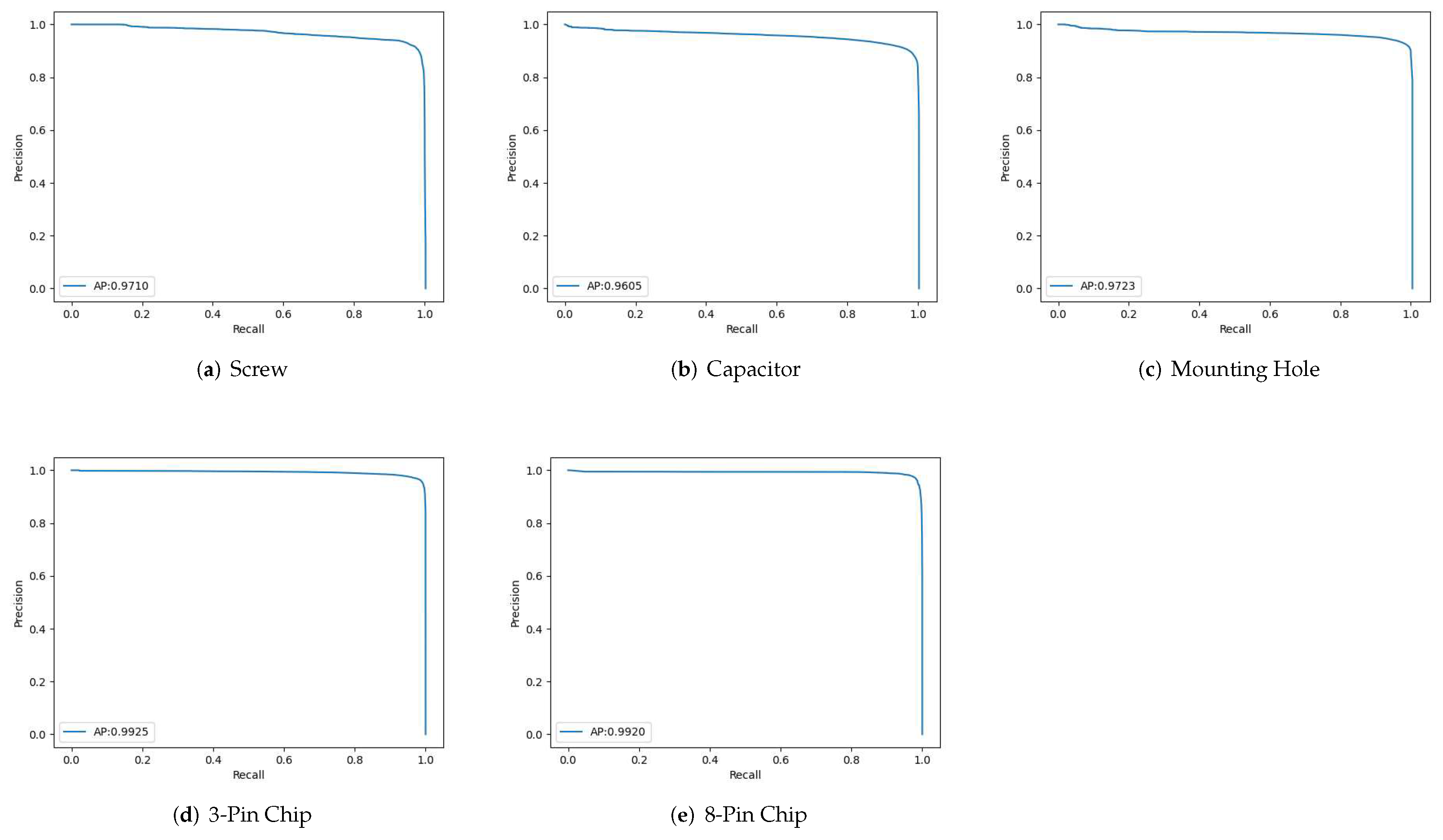
Figure 10 reveals the precision-recall curves for all the component classes considered in this study for Model 3 with two-stage training operations. It can be observed from
Figure 10 that the proposed algorithm is able to maintain high precision even with high recall value. In particular, for the class of screws, when the recall value achieves 0.916, the precision value is 0.973. Therefore, the proposed algorithm is able to achieve high detection accuracy without triggering large number of false alarms.
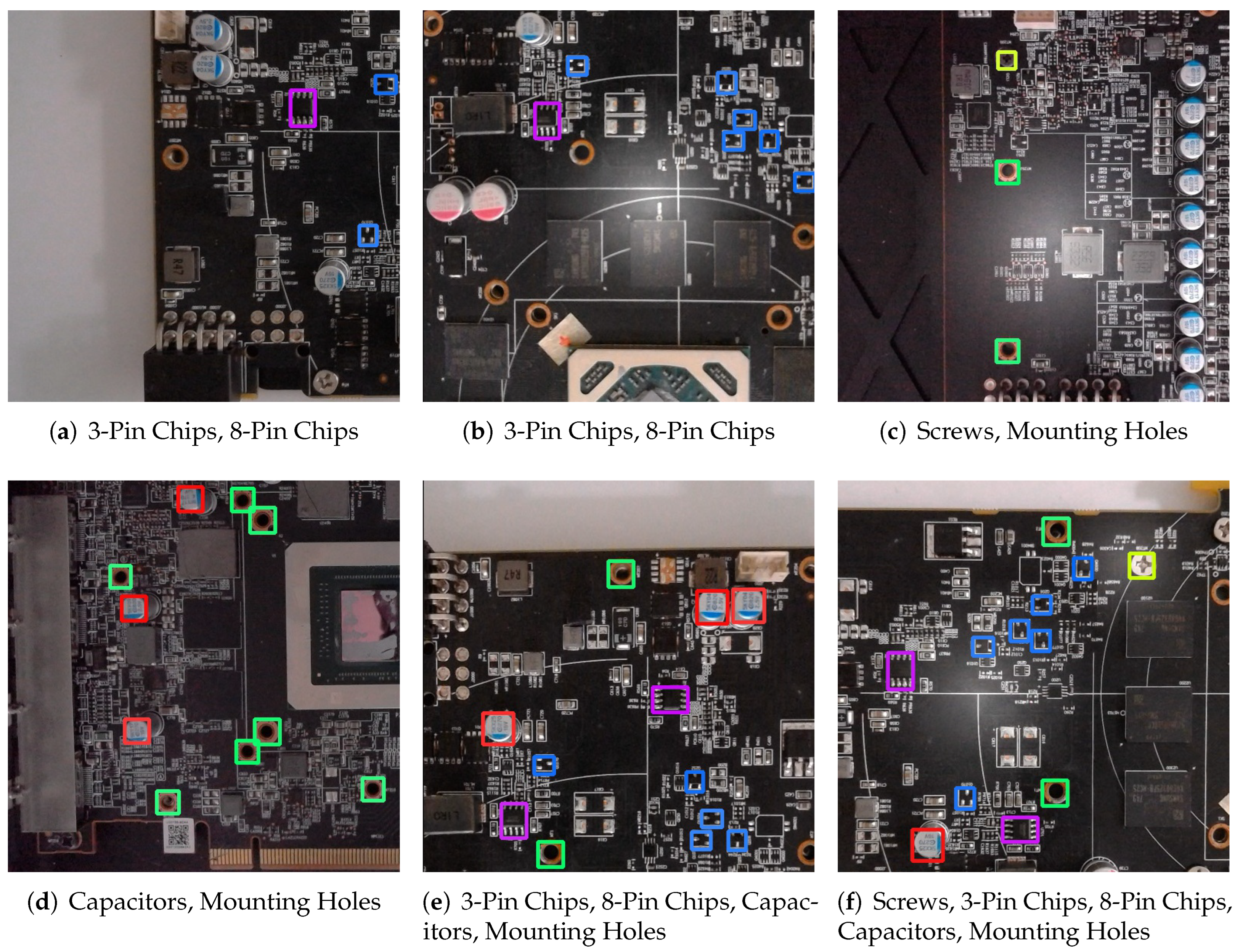
Figure 11 shows examples of the inspection results for the capacitors for different PCBs. Accurate locations and sizes of the capacitors can still be acquired even for the images from the testing set. To further demonstrate the effectiveness of the proposed algorithm,
Figure 12 reveals examples for the joint inspection for screws, capacitors, mounting holes, 3-pin chips and 8-pin chips. It can be observed from the figure that joint inspection of five components can also be effectively carried out. In fact, the sizes of some of the components such as 3-pin chips are very small so that it may be difficult to identify the components even by direct visual inspection. The proposed algorithm is able to provide accurate inspection for small components for complex backgrounds. These examples reveal that the proposed algorithm is effective for improving PCB inspection quality for automatic manufacturing in smart factory.
In
Table 5, comparisons of the proposed algorithm with existing works such as Faster Region-based Convolutional Neural Network (Faster RCNN) [
19], Single Shot Detection with MobileNet (SSD+MobileNet) [
29] and DEtection TRansformer (DETR) [
30] are made for inspection quality. Furthermore, because it is desired to deploy the NN models in embedded platforms with limited computation capacity and/or storage size, computation speed for inference and model size are then important concerns for the corresponding applications. Therefore, as shown in
Table 6, we also consider the comparisons on inference latency and model sizes among these algorithms in this study. The inference latency is measured on a Personal Computer (PC) and an embedded platform. The PC is with Intel Core I9-9900K CPU and nVidia GeForce RTX3080 Ti GPU. The embedded platform is the Jetson Nano with ARM Cortex A57 CPU and nVidia Maxwell GPU.
We can see from
Table 5 and
Table 6 that the proposed algorithm outperforms many of the existing algorithms for the inspection of components. In fact, the proposed algorithm has higher AP value and F1 score as compared with those of Faster-RCNN [
19] and SSD+MobileNet [
29] for the detection of all components. The proposed algorithm also has comparable AP values and F1 scores to those of DETR [
30]. In addition, the proposed algorithm has significantly lower inference time for PC-based inference. In particular, the inference time of the proposed algorithm and DETR are 21.4 ms and 206.5 ms for PC, respectively. The throughput (in Frames Per Second, FPS) of the proposed algorithm and DETR are then 46.73 and 4.84, respectively. The proposed algorithm has faster computation speed because it has smaller network size as compared with its DETR counterpart. In addition, it would be difficult to deploy DETR to low cost embedded devices such as Jetson Nano because of its large network size. By contrast, we have successfully deployed the proposed algorithm to Jetson Nano. The latency of the proposed algorithm for the Jetson Nano is 146.9 ms. That is, the algorithm achieves 6.81 FPS even for low-cost embedded devices. The proposed algorithm therefore has the advantages of high inspection accuracy, low inference latency, small model sizes, and low cost deployment. All these preliminary evaluations reveal that the proposed algorithm is promising for the real-time high accuracy component placement inspection.
4. Conclusions
Experimental results have shown that the proposed algorithm is effective for component displacement inspection for PCBs. The algorithm provides a simple labelling process for training. The sizes of the proposed networks are also significantly lower than existing ones. The two-stage training process is beneficial for the feature extraction for enhancing the inspection accuracy. Furthermore, the algorithm has high model reusability, and low computation complexities for inspection. Real-time component inspection with low deployment costs could then be implemented for a production line. Finally, the algorithm is able to achieve high detection accuracy even when multiple classes of components are presented on the PCBs. This advantage is beneficial for the deployment of the algorithm for component inspection over large varieties of PCBs.
Author Contributions
Conceptualization, W.-J.H. and T.-M.T.; methodology, S.-T.C. and W.-J.H.; software, S.-T.C.; validation, S.-T.C. and W.-J.H.; investigation, S.-T.C. and T.-M.T.; resources, W.-J.H.; writing—original draft preparation, W.-J.H.; writing—review and editing, W.-J.H.; visualization, S.T.-C.; supervision, W.-J.H.; project administration, W.-J.H. and T.-M.T.; funding acquisition, W.-J.H. All authors have read and agreed to the published version of the manuscript.
Funding
The original research work presented in this paper was made possible in part by National Science and Technology Council, Taiwan, under grants MOST 111-2622-E-003-001 and MOST 111-2221-E-003-009-MY2.
Institutional Review Board Statement
Not applicable.
Informed Consent Statement
Not applicable.
Data Availability Statement
The data are contained within the article.
Conflicts of Interest
The authors declare no conflict of interest. The funders had no role in the design of the study; in the collection, analyses, or interpretation of data; in the writing of the manuscript; or in the decision to publish the results.
Abbreviations
The following abbreviations are used in this manuscript:
| AP |
Average Precision |
| BN |
Batch Normalization |
| CNN |
Convolutional Neural Network |
| Conv |
2-Dimenional Convolution |
| DETR |
DEtection TRansformer |
| Faster RCNN |
Faster Region-based Convolutional Neural Network |
| FN |
False Negative |
| FP |
False Positive |
| IoT |
Internet-of-Things |
| NN |
Neural Network |
| PC |
Personal Computer |
| PCB |
Printed Circuit Board |
| ResBlock |
Residual Block |
| RELU |
REctified Linear Unit |
| SSD |
Single Shot Detection |
| TP |
True Positive |
Appendix A. Frequently Used Symbols
Table A1.
A list of symbols used in this study.
Table A1.
A list of symbols used in this study.
|
Set of training images. |
| a |
The number of training images in the training set . |
|
An augmented image randomly drawn from the set . |
|
Set of augmented images derived from the i-th image of . |
| b |
The number of augmented images in set . |
| F |
The function F denotes the frontend network. |
| H |
Hight of the input image X. |
|
Ground truth of the height of the k-th component. |
|
Estimated height of the k-th component. can be obtained from by (5). |
| K |
Number of components. |
| N |
Number of component classes for inspection. |
| P |
Number of groups. |
| R |
Output stride size. |
| S |
are the results of size estimation for components. |
|
Estimation of height of components. |
|
Estimation of width of components. |
| T |
A tuple containing elements for the first stage training. |
| X |
An input image for component placement inspection. |
|
the i-th image of the set of training images. |
| Y |
Output heatmap produced by the proposed neural network. |
|
The -th pixel of the output heatmap Y. |
| W |
Width of the input image X. |
|
Ground truth of the width of the k-th component. |
|
Estimated width of the k-th component. can be obtained from by (5). |
| Z |
Ground truth for the heatmap Y. |
|
The -th pixel of the ground truth image Z. |
References
- Szeliski, R. Computer Vision: Algorithms and Applications; Springer-Verlag: London, UK, 2011. [Google Scholar]
- Goodfellow, I.; Bengio, Y.; Courville, A. Deep Learning; MIT Press: Cambridge, MA, USA, 2016. [Google Scholar]
- Chauhan, A.P.S.; Bhardwaj, S.C. Detection of bare PCB defects by image subtraction method using machine vision. In Proceedings of the World Congress on Engineering, London, UK, 6-8 July 2011; vol. 2; pp. 6–8. [Google Scholar]
- Mogharrebi, M.; Prabuwono, A.S.; Sahran, S.; Aghamohammadi, A. Missing Component Detection on PCB Using Neural Networks. In Advances in Electrical Engineering and Electrical Machines; Zheng, D., Ed.; Lecture Notes in Electrical Engineering; Springer: Berlin/Heidelberg, Germany, 2011; vol 134. [Google Scholar]
- Tan, J.S.; Mohd-Mokhtar, R. Neural Network for the Detection of Misplaced and Missing Regions in Images. In Proceedings of the IEEE Conf. on Automatic Control and Intelligent Systems; 2017; pp. 134–139. [Google Scholar]
- Long, J.; Shelhamer, E.; Darrell, T. Fully Convolutional Networks for Semantic Segmentation. In Proceedings of the IEEE Conf. on Computer Vision and Pattern Recognition (CVPR); 2015; pp. 3431–3440. [Google Scholar]
- Ronneberger, O.; Fischer, P.; Brox, T. U-Net: Convolutional networks for biomedical image segmentation. In Proceedings of the Int. Conf. Medical Image Computing and Computer-Assisted Intervention; 2015. [Google Scholar]
- Lim, D.U.; Kim, Y.G.; Park, T.H. SMD classification for automated optical inspection machine using convolution neural network. In Proceedings of the IEEE Int. Conf. Robotic Computing (IRC), Naples, Italy; 2019; pp. 395–398. [Google Scholar]
- Li, D.; Li, C.; Chen, C.; Zhao, Z. Semantic Segmentation of a Printed Circuit Board for Component Recognition Based on Depth Images. Sensors 2020, 8, 5318. [Google Scholar] [CrossRef] [PubMed]
- Krawczyk, B. Learning from imbalanced data: open challenges and future directions. Progress in Artificial Intelligence 2016, 5, 221–232. [Google Scholar] [CrossRef]
- Lin, T.Y.; Goyal, P.; Girshick, R.; He, K.; Dollar, P. Focal Loss for Dense Object Detection. arXiv Preprint 2017, arXiv:1708.02002. [Google Scholar]
- Lai, C.W.; Zhang, L.; Tai, T.M.; Tsai, C.C.; Hwang, W.J.; Jhang, Y.J. Automated Surface Defect Inspection Based on Autoencoders and Fully Convolutional Neural Networks. Applied Sciences 2021, 11, 7838. [Google Scholar] [CrossRef]
- Lin, Y.L.; Chiang, Y.M.; Hsu, H.C. Capacitor Detection in PCB Using YOLO Algorithm. In Proceedings of the IEEE Int. Conf. System Science and Engineering; 2018. [Google Scholar]
- Jiao, L.; Zhang, F.; Liu, F.; Yang, S.; Li, L.; Feng, Z.; Qu, R. A Survey of Deep Learning Based Object Detection. IEEE Access 2019, 7, 128837–128868. [Google Scholar] [CrossRef]
- Adibhatla, V.A.; Chih, H.-C.; Hsu, C.-C.; Cheng, J.; Abbod, M.F.; Shieh, J.S. Defect Detection in Printed Circuit Boards Using You-Only-Look-Once Convolutional Neural Networks. Electronics 2021, 9, 1547. [Google Scholar] [CrossRef]
- Li, J.; Li, W.Y.; Chen, Y.; Gu, J. A PCB Electronic Components Detection Network Design Based on Effective Receptive Field Size and Anchor Size Matching. Computational Intelligence and Neural Science 2021. [Google Scholar] [CrossRef] [PubMed]
- Ren, S.; He, K.; Girshick, R.; Sun, J. Faster R-CNN: Towards Real- Time Object Detection with Region Networks. In Proceedings of the Advances in Neural Information Processing Systems (NIPS); 2015. [Google Scholar]
- Fu, C.Y.; Liu, W.; Ranga, A.; Tyagi, A.; Berg, A.C. DSSD: Deconvolutional Single Shot Detector. arXiv Preprint 2017, arXiv:1701.06659. [Google Scholar]
- Huang, J.; Rathod, V.; Sun, C.; Zhu, M.; Korattikara, A.; Fathi, A.; Fischer, I.; Wojna, Z.; Song, Y.; Guadarrama, S.; Murphy, K. Speed/accuracy trade-offs for modern convolutional object detectors. In Proceedings of the IEEE Conf. on Computer Vision and Pattern Recognition (CVPR); 2017. [Google Scholar]
- Kuo, C.W.; Ashmore, J.D.; Huggins, D.; Kira, Z. Data-Efficient Graph Embedding Learning for PCB Component Detection. In Proceedings of the Winter Conf. Applications of Computer Vision; 2019. [Google Scholar]
- Zhou, X.; Wang, D.; Krahenbuhl, P. Objects as Points. arXiv Preprint 2019, arXiv:1904.07850v1. [Google Scholar]
- Law, H.; Deng, J. CornerNet: Detecting Objects as Paired Keypoints. In Proceedings of the European Conf. Computer Vision; 2018; pp. 734–750. [Google Scholar]
- Duan, K.; Bai, S.; Xie, L.; Qi, H.; Huang, Q.; Tian, Q. CenterNet: Keypoint Triplets for Object Detection. arXiv Preprint 2019, arXiv:1904.08189. [Google Scholar]
- Sohn, K. Improved Deep Metric Learning with Multi-class N-pair Loss Objective. In Proceedings of the Advances in Neural Information Processing Systems; 2016. [Google Scholar]
- Wu, Z.; Shen, C.; van den Hengel, A. Wider or Deeper: Revisiting the ResNet Model for Visual Recognition. Pattern Recognit. 2019, 90, 119–133. [Google Scholar] [CrossRef]
- Chen, C.; Tian, X.; Xiong, Z.; Wu, F. UDNet: Up-Down Network for Compact and Efficient Feature Representation in Image Super-Resolution. In Proceedings of the IEEE Int. Conf. on Computer Vision (ICCV), 2017; pp. 1069-1076. [Google Scholar]
- Goutte, C.; Gaussier, E. A Probabilistic Interpretation of Precision, Recall and F-Score, with Implication for Evaluation. Lecture Notes in Computer Science 2005, 3408, 345–359. [Google Scholar]
- Boyd, K.; Eng, K.H.; Page, C.D. Area under the Precision-Recall Curve: Point Estimates and Confidence Intervals. Lecture Notes in Computer Science 2013, 8190, 451–466. [Google Scholar]
- Sandler, M.; Howard, A.; Zhu, M.; Zhmoginov, A.; Chen, L.C. MobileNetV2: Inverted Residuals and Linear Bottlenecks. In Proceedings of the IEEE Conf. on Computer Vision and Pattern Recognition (CVPR); 2018. [Google Scholar]
- Carion, N.; Massa, F.; Synnaeve, G.; Usunier, N.; Kirilov, A.; Zagoruyko, S. End-to-End Object Detection with Transformers. arXiv Preprint 2020, arXiv:2005.12872. [Google Scholar]
Figure 1.
The block diagram of proposed NN model for the single-class component detection.
Figure 1.
The block diagram of proposed NN model for the single-class component detection.
Figure 2.
An example showing the keypoint of a component. In the example, the screw on the image is the target component to be inspected. The centroid of the screw is the keypoint.
Figure 2.
An example showing the keypoint of a component. In the example, the screw on the image is the target component to be inspected. The centroid of the screw is the keypoint.
Figure 3.
An example of ground truth of heatmap for the inspection of capacitors on a PCB.
Figure 3.
An example of ground truth of heatmap for the inspection of capacitors on a PCB.
Figure 4.
Three network models for the multi-class component placement inspection.
Figure 4.
Three network models for the multi-class component placement inspection.
Figure 5.
Examples of frontend and backend networks for a single class, where each Conv layer is a 2-dimentional convolution layer, and each Conv Trans layer is a 2-dimensional transposed convolution layer. In addition, ResBlock is a residual block with a short cut, BN denotes Batch Normalization, and RELU is an activation function.
Figure 6.
The setup of the experiment. A high resolution industrial camera is adopted for the acquisition of images from the PCBs.
Figure 6.
The setup of the experiment. A high resolution industrial camera is adopted for the acquisition of images from the PCBs.
Figure 7.
The component classes considered in the experiments.
Figure 7.
The component classes considered in the experiments.
Figure 8.
Examples of different cropping results for the training images.
Figure 8.
Examples of different cropping results for the training images.
Figure 9.
Test PCBs considered in this study. The test images are acquired from the PCBs.
Figure 9.
Test PCBs considered in this study. The test images are acquired from the PCBs.
Figure 10.
Precision-Recall curves of the five component classes considered in this study. The corresponding network model is Model 3 with two-stage training process.
Figure 10.
Precision-Recall curves of the five component classes considered in this study. The corresponding network model is Model 3 with two-stage training process.
Figure 11.
Examples of the inspection results for the capacitors for different PCBs.
Figure 11.
Examples of the inspection results for the capacitors for different PCBs.
Figure 12.
Examples for the joint inspection for screws, capacitors, mounting holes, 3-pin chips and 8-pin chips.
Figure 12.
Examples for the joint inspection for screws, capacitors, mounting holes, 3-pin chips and 8-pin chips.
Table 1.
The parameters of the example model containing only one frontend network and one backend network for a single class inspection. The names of layers are defined in
Figure 5. The layer size and network size are the number of weights for a layer and a network, respectively.
Table 1.
The parameters of the example model containing only one frontend network and one backend network for a single class inspection. The names of layers are defined in
Figure 5. The layer size and network size are the number of weights for a layer and a network, respectively.
| Network |
Frontend Network |
Backend Network |
| Layer |
Conv 1 |
Resblock 1 |
Resblock 2 |
Conv Trans 1 |
Conv Trans 2 |
Conv 2 |
Conv 3 |
Conv 4 |
Conv 5 |
Conv 6 |
Conv 7 |
| Stride Size |
2 |
2 |
2 |
2 |
2 |
1 |
2 |
1 |
1 |
1 |
1 |
| Kernel Size |
|
|
|
|
|
|
|
|
|
|
|
| Input Tensor |
|
|
|
|
|
|
|
|
|
|
|
| Dimension |
3 |
32 |
64 |
128 |
128 |
64 |
64 |
64 |
128 |
64 |
128 |
| Layer Size |
4,736 |
29,856 |
119,104 |
147,584 |
73,792 |
36,928 |
36,928 |
73,856 |
129 |
73,856 |
258 |
| Network Size |
452,128 |
148,099 |
Table 2.
The specifications of the proposed NN models for the inspection of 5 component classes. The model size is defined as the number of weights in the whole model.
Table 2.
The specifications of the proposed NN models for the inspection of 5 component classes. The model size is defined as the number of weights in the whole model.
| Model Type |
Model 1 |
Model 2 |
Model 3 |
| Input X Dimension |
|
|
|
| Output Y Dimension |
|
|
|
| Output S Dimension |
|
|
|
| Model Size |
600,743 |
1,192,623 |
1,644,751 |
| Model Configuration |
1 Frontend NN |
1 Frontend NN |
2 Frontend NNs |
| |
1 Backend NN |
5 Backend NN |
5 Backend NNs |
Table 3.
The inspection accuracy of various component classes of the Model 1 with single-stage and two-stage training processes.
Table 3.
The inspection accuracy of various component classes of the Model 1 with single-stage and two-stage training processes.
| Training Process |
Inspection Accuracy |
Screw |
Mounting Hole |
Capacitor |
3-pin Chip |
8-pin Chip |
| Single-Stage |
AP |
0.9460 |
0.9316 |
0.9391 |
0.9682 |
0.9665 |
| [21] |
F1 |
0.9283 |
0.8876 |
0.8867 |
0.9123 |
0.9055 |
| Two-Stage |
AP |
0.9695 |
0.9400 |
0.9532 |
0.9801 |
0.9755 |
| |
F1 |
0.9482 |
0.8912 |
0.9320 |
0.9429 |
0.9296 |
Table 4.
The AP values and F1 scores of various component classes for Model 1, Model 2 and Model 3. The two-stage training process is employed for the models.
Table 4.
The AP values and F1 scores of various component classes for Model 1, Model 2 and Model 3. The two-stage training process is employed for the models.
| Component Class |
Model 1 |
Model 2 |
Model 3 |
| |
AP |
F1 |
AP |
F1 |
AP |
F1 |
| Capacitor |
0.9532 |
0.9320 |
0.9739 |
0.9368 |
0.9605 |
0.9363 |
| Screw |
0.9695 |
0.9482 |
0.9709 |
0.9453 |
0.9710 |
0.9435 |
| 3-pin Chip |
0.9801 |
0.9429 |
0.9930 |
0.9734 |
0.9925 |
0.9739 |
| 8-pin Chip |
0.9755 |
0.9296 |
0.9892 |
0.9662 |
0.9920 |
0.9760 |
| Mounting Hole |
0.9400 |
0.8912 |
0.9437 |
0.9437 |
0.9723 |
0.9545 |
Table 5.
The inspection accuracy of various component classes for various algorithms.
Table 5.
The inspection accuracy of various component classes for various algorithms.
| Training Process |
Inspection Accuracy |
Screw |
Mounting Hole |
Capacitor |
3-pin Chip |
8-pin Chip |
| Proposed |
AP |
0.9710 |
0.9723 |
0.9605 |
0.9925 |
0.9920 |
| Model 3 |
F1 |
0.9435 |
0.9545 |
0.9363 |
0.9739 |
0.9760 |
| Faster RCNN |
AP |
0.9680 |
0.9335 |
0.9523 |
0.9734 |
0.9895 |
| [19] |
F1 |
0.9078 |
0.8755 |
0.9018 |
0.9363 |
0.9702 |
| SSD + MobileNet |
AP |
0.9218 |
0.8986 |
0.9459 |
0.9585 |
0.9799 |
| [29] |
F1 |
0.8425 |
0.8610 |
0.8930 |
0.9042 |
0.9833 |
| DETR |
AP |
0.9800 |
0.9472 |
0.9641 |
0.9944 |
0.9986 |
| [30] |
F1 |
0.9469 |
0.9341 |
0.9389 |
0.9735 |
0.9946 |
Table 6.
The weight sizes and computation time for inference for various algorithms.
Table 6.
The weight sizes and computation time for inference for various algorithms.
| Algorithm |
Weight Size |
Inference Latency |
| |
|
PC |
Jetson Nano |
| Proposed (Two-Stage) |
1,644,751 |
21.4 ms |
146.9 ms |
| Faster RCNN [19] |
28,337,682 |
56.1 ms |
NA |
| SSD + MobileNet [29] |
2,601,212 |
46.4 ms |
167.6 ms |
| DETR [30] |
41,487,306 |
206.5 ms |
NA |
|
Disclaimer/Publisher’s Note: The statements, opinions and data contained in all publications are solely those of the individual author(s) and contributor(s) and not of MDPI and/or the editor(s). MDPI and/or the editor(s) disclaim responsibility for any injury to people or property resulting from any ideas, methods, instructions or products referred to in the content. |
© 2023 by the authors. Licensee MDPI, Basel, Switzerland. This article is an open access article distributed under the terms and conditions of the Creative Commons Attribution (CC BY) license (http://creativecommons.org/licenses/by/4.0/).

