1. Introduction
With the advancement in semiconductor technology, highly integrated and miniaturized designs of semiconductors are being used to improve the overall performance of the device. In this regard, the high-aspect-ratio (HAR) patterns prevail with the aim to reduce critical dimensions in the current semiconductor manufacturing processes. Plasma etching techniques like reactive ion etching (RIE), which employs reactive ionized gases in the plasma, are used for HAR patterning. Studies have examined the importance of suppressing lateral etching and increasing vertical etching in HAR silicon etching so as to achieve a smooth vertical sidewall profile with high etch rate and selectivity [
1]. When the aspect ratio of the etch pattern is increased, 3D-NAND flash memory products have exhibited feature distortions, such as twisting, bowing, and edge roughening [
2]. These etch pattern distortion problems are caused by the energetic ions in the plasma, as observed in the retarded etch rate in the high-aspect-ratio contact (HARC) pattern etch process due to ion charging inside shallow and deep contract holes. This etch rate retardation can be overcome by employing high-frequency bias power in semiconductor etch equipment to increase plasma potential in HARC pattern etch so as to increase the ion bombardment energy across the plasma sheath. Ion energy distribution and ion angular distribution that enters a wafer perpendicular to the plasma sheath surface are controlled using low-frequency bias power [
3,
4]. When the bias power is increased to the level of a few kilo Watts, surface collision with the wafer surface increases, causing the heated ions to become uncontrollable and result in the distorted etch sidewall profile. From the thermal perspective, the increased wafer surface temperature may lead to undesirable chemical reactions, and the thermal stress caused by temperature variation or differences in coefficient of thermal expansion in 3D multilayer structures such as ONO stack process may lead to wafer warpage [
5,
6].
The etched feature profile and critical dimension uniformity are controlled via the temperature of wafer-in-process (WIP) [
7]. Wafer-temperature uniformity can create multiple integrated circuits (ICs) that have the etch profiles required for a wafer. Research is being conducted to control wafer-temperature uniformity from the component perspective. In the case of electrostatic chuck that is in direct contact with the wafer, an excellent etching profile is generated by improving WIP temperature uniformity through a cryogenic environment [
8]. Studies have also proposed methods to improve WIP temperature uniformity based on the heat transfer or the cooling path shape of the chuck for the contact region between electrostatic chuck and wafer [
9,
10,
11,
12]. In addition, the wafer-temperature uniformity is also improved by tuning the height and the baffle shape of the edge ring [
13]. Previous research works have showed that controlling WIP temperature is a key parameter to ensure the etching profile in HARC.
Etch process employs reactive ionized gas species, such as SF6, Cl2, or C4F8 with a mixture of additive gases of O2, N2, He, Ar, etc. The ratio and flow rate of the injected gases affect the etch rate and uniformity [
14,
15,
16]. This shows that both the physical reaction of the inert gas and the chemical reaction of the reactive gas on the wafer surface should be considered in the etch process. Excessive chemical reactions in procedures requiring anisotropic etch may result in poor surface uniformity and rough sidewalls due to the isotropic etch and unpredictable radical movement [
17]. Thus, the parameters that affect temperature changes need to be optimized to control temperature-sensitive chemical reactions. Temperature source like chuck temperature and chamber wall temperature might indirectly affect WIP temperature during the etching process [
18,
19]. Ion generated from plasma can directly affect WIP temperature. When ions fall from the plasma to the wafer surface, ion bombardment occurs in which the energy of the ions is transferred by converting them into thermal energy [
20,
21].
Heat flux refers to the transfer rate of thermal energy in the unit area per unit time with a physical metric unit of W/m2. The heat flux directly affecting WIP temperature from the plasma side surface can be calculated by analyzing the ions. The heat flux from the plasma to the wafer consist of parameters such as the energy of ions and the density of ions [
22]. It is essential to determine the effect of changes in process parameters on the ion characteristics in plasma so as to accurately calculate heat flux. With the increase or decrease in the collision of ions in the sheath according to the changes in the mean free path, the source power affects ion density as it controls plasma density, the bias power influences ion energy, and the pressure affects etch rate and etch profile [
23]. Thus, the etch profile can be altered depending on the ion energy distribution based on plasma properties or the ion angle distribution applied to the wafer, as shown above [
24]. The WIP temperature must be analyzed and controlled to enhance the etching rate and improve uniformity [
25]. Different methods such as optical thermometer, thermal flux sensor, and wafer-type monitoring apparatus, have been proposed for analyzing WIP temperature [
26,
27,
28,
29]. In the present study, heat flux was calculated using inductive coupled plasma (ICP)-RIE equipment in a invasive way to predict wafer surface temperature. In addition, the parameters required for calculation were compared using optical emission spectroscopy (OES) and single Langmuir probe (SLP), and the calculation was verified through etch-temp-sensor-wafer (ETSW). The remaining sections of this study are detailed as follows: Section II describes theory related to heat flux, Section III describes experimental apparatus, and Section IV explains the results, and Section V presents the conclusions of this study.
2. Theory
2.1. Heat Flux Calculation Method
Heat fluxes are compared using two models. First, the model can be expressed as follows [
30].
where
denotes the total heat influx,
denotes the heat capacity of the wafer, and
denotes surface wafer-temperature. The total heat flux value is calculated using the difference between the initial wafer-temperature and the temperature after the process, and the heat capacity of the wafer. In this calculation, energy transfer efficiency is considered to substantially apply the ion bombardment energy transfer from plasma to the wafer [
31]. The energy transfer efficiency from ions of a specific gas to the wafer is given as follows.
where
denotes the energy transfer efficiency, and
denotes the mass ratio of bombarding ion (
to Si atom (
, as presented in the following equation.
In addition, the effect of energy-transfer due to the angle at which ions enter the wafer cannot be ignored, and the angle of incidence is assumed to be θ = 90° through the low-pressure condition.
The second model calculates the heat flux incident from the plasma to the wafer and can be expressed as follows.
where
denotes the total plasma heat flux incident on the wafer,
denotes the total energy influx, and
denotes wafer surface area. The total energy influx parameter should be comprehended and calculated to determine the plasma heat flux. Total energy influx is expressed as follows.
where
denotes energy flux due to ion,
denotes energy flux due to electron,
denotes energy flux of neutrals due to electron and vibration excitation,
denotes energy flux of reactions associated with other gas phases, and
denotes energy flux due to chemical reaction in wafer surface. However, this study considers only the physical reaction of ions, which is the main parameter of anisotropic etching and increasing wafer-temperature required according to HAR. The term summarizing the ion energy flux is as follows.
where
denotes kinetic energy of ion, and
is energy balance of the substrate due to recombination. The two terms can be expressed as follows.
Kinetic energy of ion consists of ion flux density
and ion mean energy
, and the recombination energy of ion is replaced by ionization energy
instead of ion mean energy. The expression of ion flux density is used according to the pressure or other conditions. The Bohm-flux equation expressed in Eqn. (9) was utilized since it is used in the target process at a low-pressure (<10 Pa). In addition, ion mean energy may be expressed as a difference between plasma potential
and bias potential
, as shown in Eqn. (10).
With reference to
Figure 1, the plasma characteristics for potential leak (
) are considered and applied [
32]. Applying Eqn. (11) to Maxwellian electron energy distribution function (EEDF) in Eqn. (7) of kinetic energy of ion, the final equation to obtain plasma heat flux may be expressed as follows.
Thus, electron density () and electron temperature () are the main parameters of the finally organized heat flux equation.
2.2. OES Line Ratio Method
As described above, the major plasma parameters for plasma heat flux value are compared using OES. The OES sensor monitors the intensity of a particular wavelength produced by an excited electron of an atom as it transitions back to its ground state in plasma. Although OES measures optics, the values of electron density and electron temperature can also be obtained using the line-ratio method. The line-ratio method is categorized into a corona model and a collisional-radiative model (CRM). The corona model has low electron density and high electron temperature and is used under very low-pressure (<1 Pa) and low ionization ratio (<10−5) conditions. In comparison, the CRM model has wider applications. The CRM model has high electron density and low electron temperature and is used under relatively high pressure (1–10 Pa) conditions and high ionization ratio (>10−5). The CRM was used in this study because of its suitable pressure and argon discharge conditions required for the calculation of the plasma heat flux.
In the case of excited argon atoms, electron impact excitation and spontaneous radiation are the dominant processes at low-pressure. The concentration of atoms in excited states is calculated by the ratio of electron impact excitation (
rate coefficient to the sum of electron impact de-excitation (
rate coefficient and spontaneous radiation (
rate coefficient. Therefore, it is a function of electron density and electron temperature; in addition, the intensity ratio of the two emission lines is a function of two parameters [
33]. By using the ratio coefficient and the ratio balance equation of the electron impact process of the corona model, Q is expressed as follows.
Here
denotes electron kinetic energy,
denotes electron mass,
EEDF, and
denotes the cross-section of the relevant electron impact process. CRM is considered because of the high-lying
ns or
nd level, unlike the process in the corona model. Other than these reactions, electron impact transition between excited levels (
and radiation trapping process (
are complicated and difficult to consider. Therefore, to simplify CRM, excitation from metastable in rate balance equation should be ignored by selecting a specific np level, a zero total angle momentum quantum number (
) of argon gas. Make a note that data for argon
p levels with
were quoted from the previous research work [
33]. Thus, when
, the total excitation rate coefficient is summarized as follows [
34].
where
denotes the sum of
(ground state to np levels) and
(ground state to high-lying
ns and
nd levels). The constants
,
and
can be found in [
33], and rate equation is expressed as follows.
where
denotes the electron density,
denotes gas density,
denotes total Einstein coefficient,
denotes the population density of species, and
denotes the characteristic density of electron impact transition. The final equation of electron density and temperature according to the intensity ratio using the preceding equations is expressed as follows.
where
denotes intensity ratio of different emission line of argon, and
denotes the branching ratio of emission lines.
3. Experimental apparatus
3.1. Experimental Equipment and Sensor Used
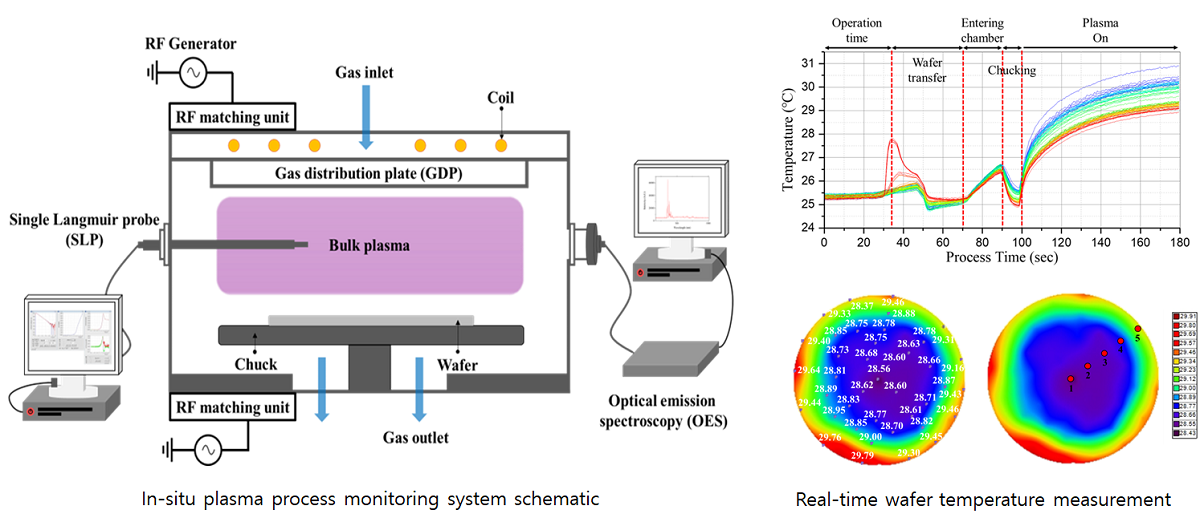
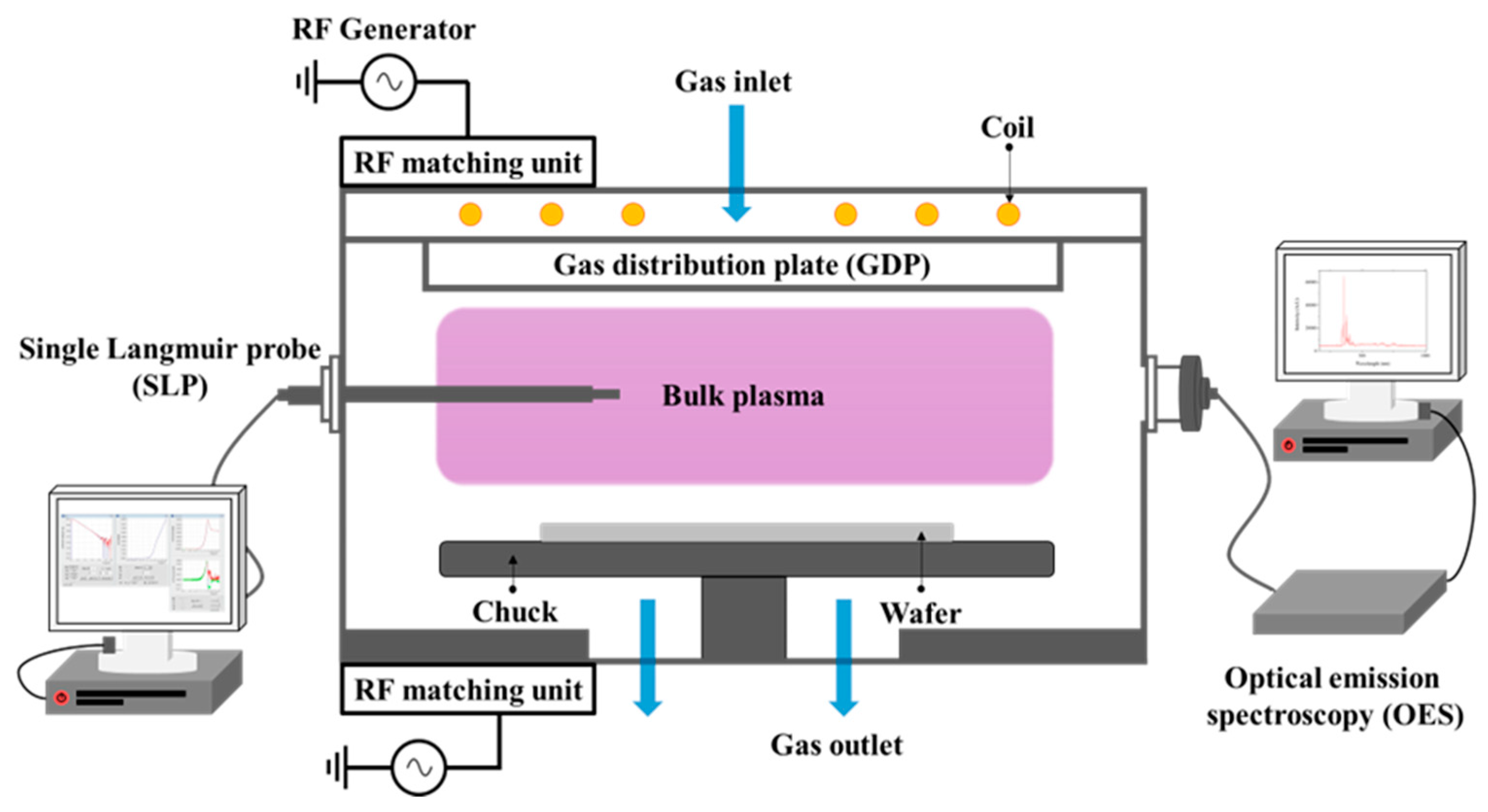
Figure 2 illustrates the experimental procedure followed in the study. As shown in the figure, plasma was generated using an ICP-RIE, developed by Plasmart, Daejeon, Korea. The ICP source power was 13.56 MHz, bias power was 12.56 MHz, and the RF matching unit was configured. The vacuum system comprised a roughing pump and a turbo molecular pump so as to set-up and maintain a low-pressure environment of tens of mTorr or less. In the case of process gas, a gas distribution plate located above the chamber is injected into the chamber by a set value through a mass flow controller. There are two viewports in the sidewall of the chamber. To conduct the experiment, an OES sensor, which is a non-invasive method for diagnosing plasma, was mounted on the front part, and an SLP, which is an invasive method, was mounted on the side part of the chamber. OES used the SM245 (Korea Spectral Products; Seoul, Korea), which has an optical resolution range of up to less than 10 nm and a measurable wavelength range of 200 nm to 1050 nm. By using the controller and the Wise Probe from P&A Solutions Product, SLP acquired data on
and
by monitoring the electron energy probability function (EEPF), the current-voltage (I-V) curve, and harmonics.
3.2. Experiment 1: OES Wavelength Selection
The experiment is categorized into a preliminary experiment for OES data analysis for wavelength selection and a main experiment for heat flux calculation. In the preliminary experiment, a 6-inch dummy wafer was placed on the chuck, and then Ar gas was injected into the chamber to discharge plasma. To select an appropriate wavelength, a wavelength value with a certain trend should be determined and then the line-ratio should be analyzed without a dramatic difference in intensity tendency despite changes in process parameters. Therefore, the Ar flow rate was fixed, and the pressure and source power were selected for the process parameter so as to select the wavelength. This is because light emission is caused by excitation and de-excitation reactions that require specific energy. At this point, the reaction is mainly caused by the mean free path value. The pressure and source power parameters affect the density of plasma, which in turn affects the mean free path. Therefore, gas density was set, and the source power and pressure parameters were chosen so as to determine the amount of energy transfer that generates a reaction. Pressure was split in units of 10 mTorr from 30 mTorr to 70 mTorr, and source power was split in the incremental step of 100 W from 100 W to 300 W. Wavelength data collection through the OES sensor was conducted and analyzed.
3.3. Experiment 2: SLP vs OES
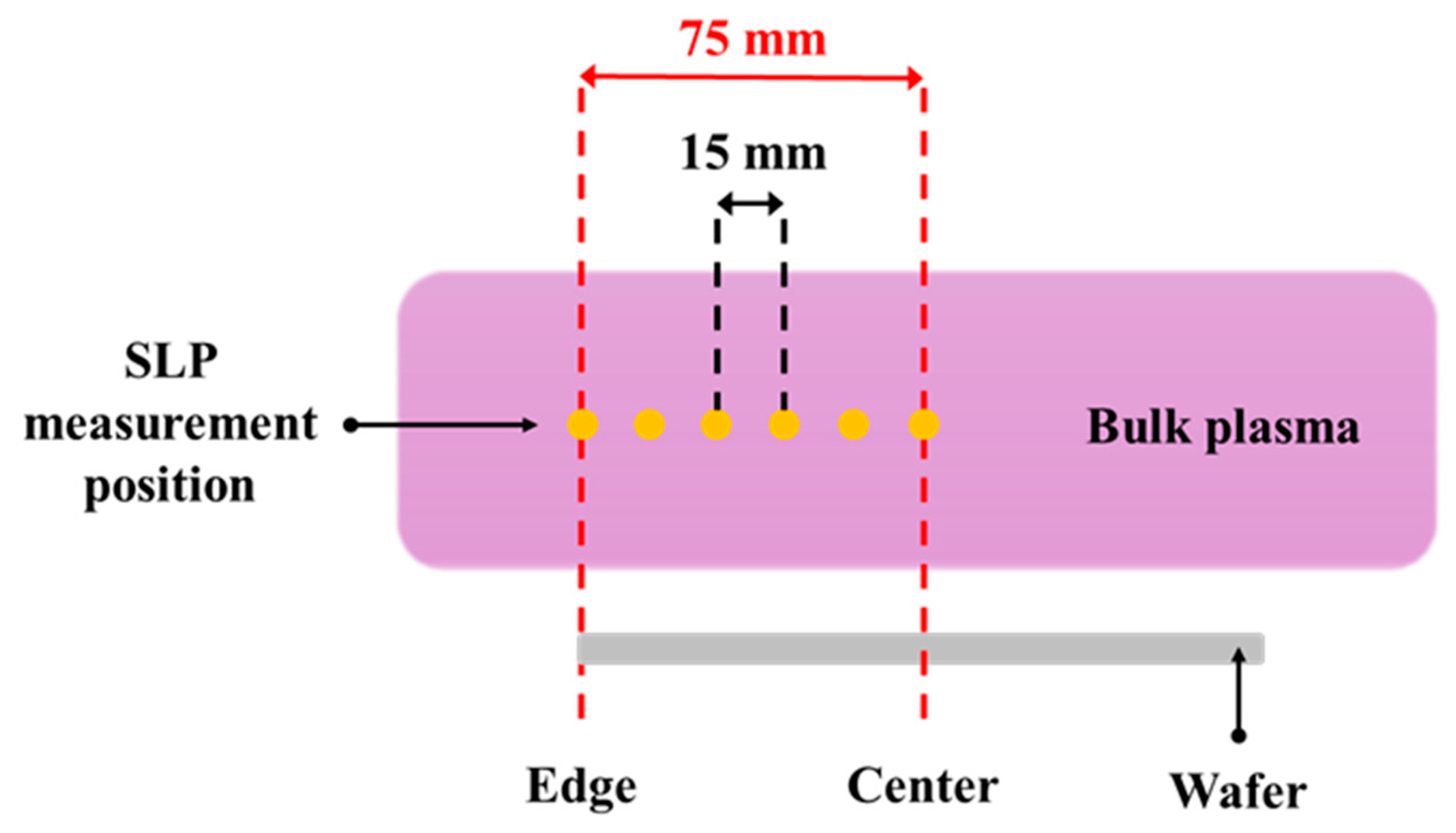
Table 1 presents the experimental process. The RF source power was set to be 200 W, the Ar flow rate was set to 30 sccm, and the temperature was set to room temperature. As a preliminary experiment, the pressure range was determined to understand the plasma characteristics, and the SLP was moved by 15 mm in the radial direction as it was 75 mm up to the center-to-edge based on the 6-inch wafer. The relative altitude value from the ESC of the SLP tip performed in the experiment is 25 mm.
Figure 3 shows the SLP measurement positions at distances of 0 mm, 15 mm, 30 mm, 45 mm, 60 mm, and 75 mm in bulk plasma. An experiment was carried out by setting bias power to 10 W, 30 W, and 50 W depending on the location alone under a pressure condition of 30 mTorr to consider the effect of bias power, which is a crucial parameter in the etching process. Additionally, the heat flux according to radial position was compared and confirmed using OES and KLA’s ETSW in a 12-inch mass production equipment, Lam Research Kiyo 45, to confirm the heat flux produced from OES and SLP data. The ETSW monitors the temperature before and after the wafer process by using wireless communication in real-time. Its temperature range is 20°C to 140°C and is measured by 65 IC temperature sensors, with a sensor accuracy of ±0.2°C.
3.4. Experiment 3: ESTW vs OES
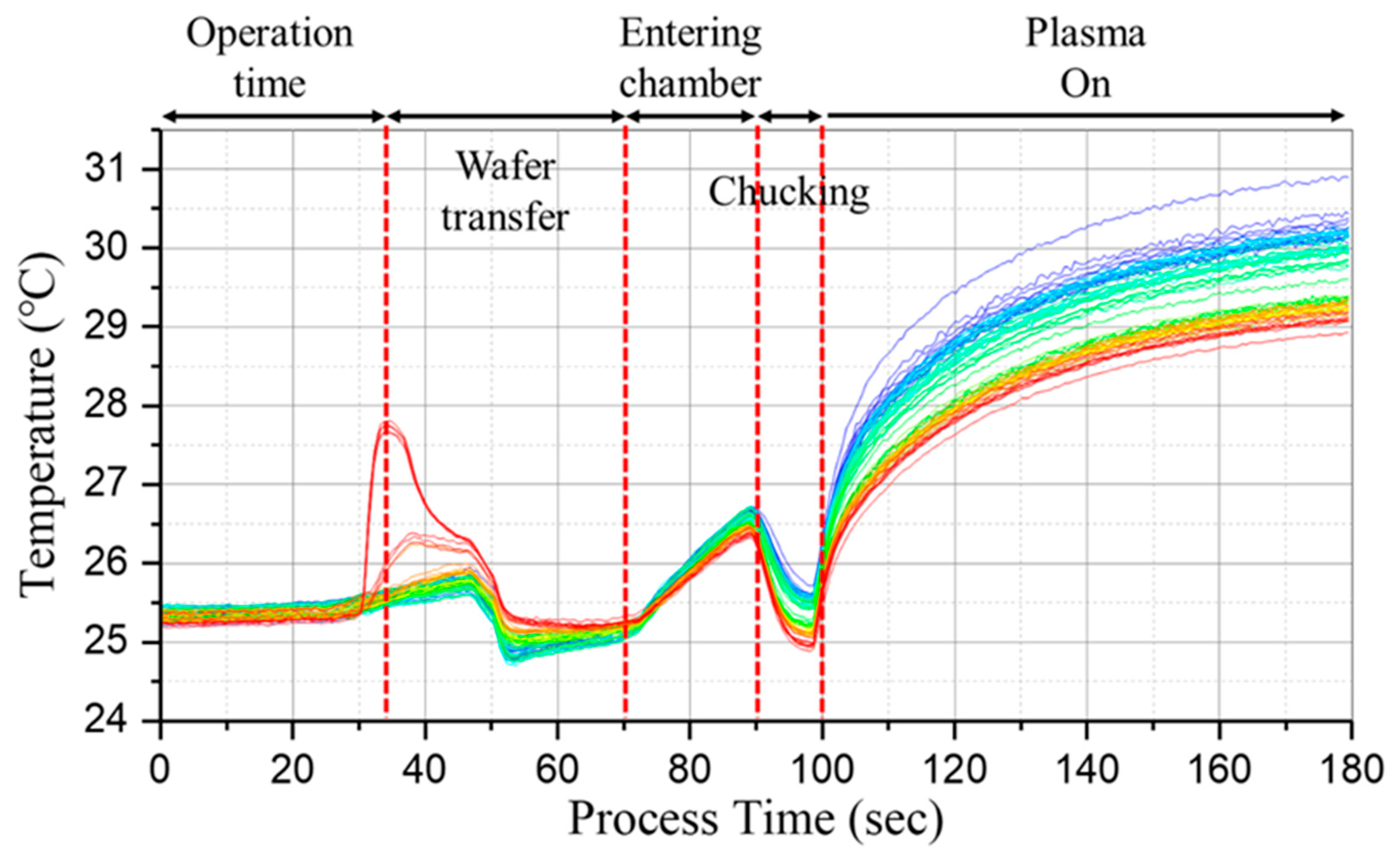
Compared to the ICP-RIE chamber that uses a 6-inch wafer, the ETSW sensor measures the WIP temperature in mass production equipment using a 12-inch wafer. The ETSW was used in an experiment in a 12-inch etcher environment to verify the suitability of the energy influx value derived from sensors in a changed environment. The experimental recipe was the same as that followed for the 6-inch wafer. The ETSW measurement includes temperature trigger and recording delay methods. In this study, we used the recording delay method, which automatically measures after the set time. First, the time (100 seconds) taken by plasma to be generated after sensor operation was confirmed through 180 seconds of pre-sensor data measurement, as shown in
Figure 4. The recording delay time was set to 250 seconds to receive wafer-temperature data for 5 seconds after 150 seconds of plasma generation. OES data was obtained through an operating program using an OES sensor installed in the equipment.
4. Result and Discussion
4.1. Experimental Result
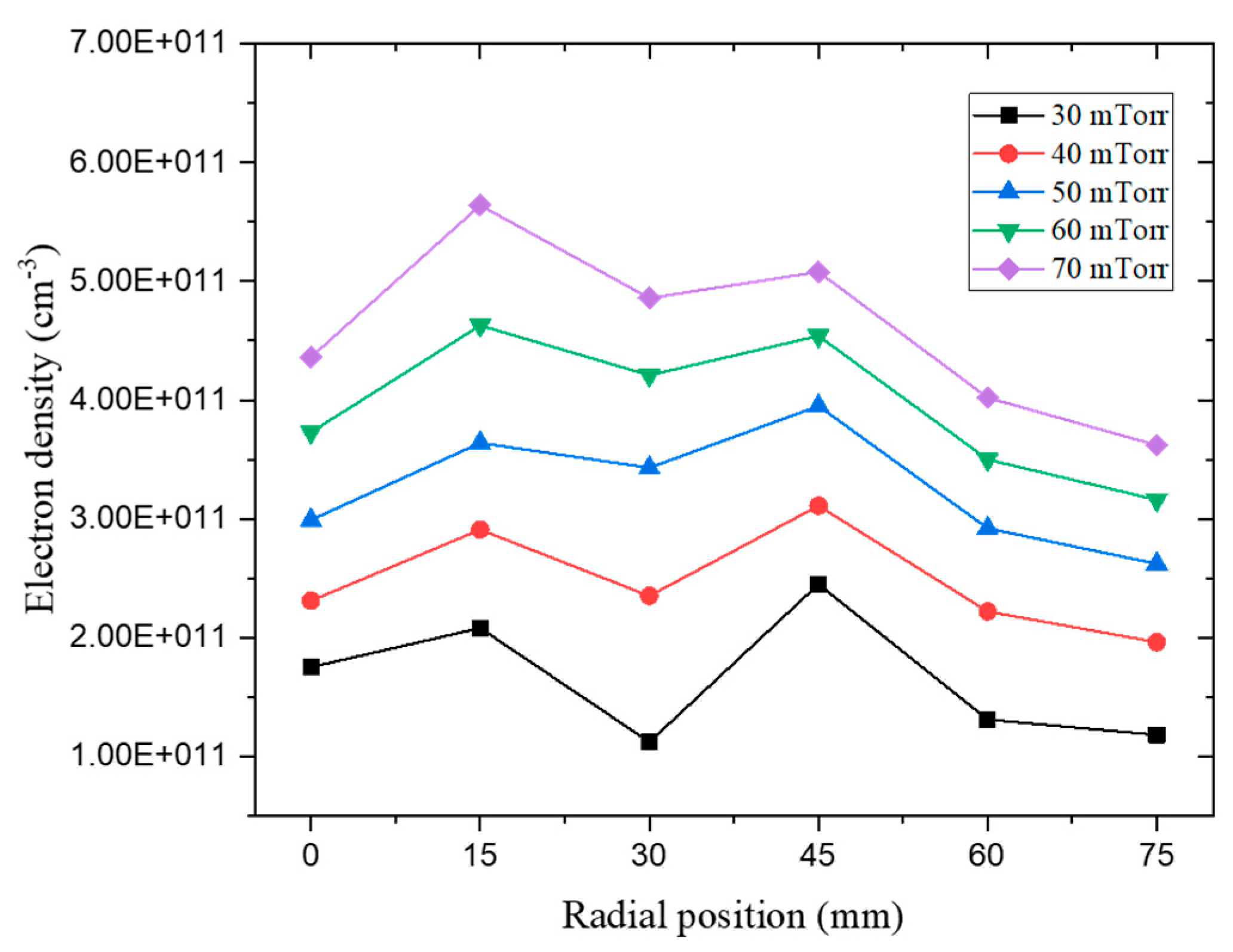
The electron density values of the radial position according to the pressure variation in the experiment using SLP is shown in
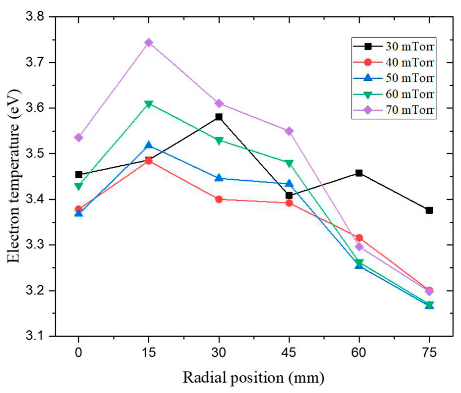
Figure 5. In the experimental data, the electron density shows a similar trend across all ranges and tends to increase at each radial position as the pressure increases. The electron temperature values of the radial position according to the pressure variation in the experiment using SLP is shown in
Figure 6. In the experiment, except for the data value at 30 mTorr, the electron temperature shows an increasing tendency at 15 mm radial position and then decreases continuously to the edge. Based on the pressure range, the electron temperature generally tends to gradually decrease from the center to the edge, and the plasma density at the center is typically larger than that at the edge [
35,
36]. Our results confirmed that the plasma parameters in bulk plasma are dominant in source power, and bias power cannot affect the parameters when compared to source power [
23].
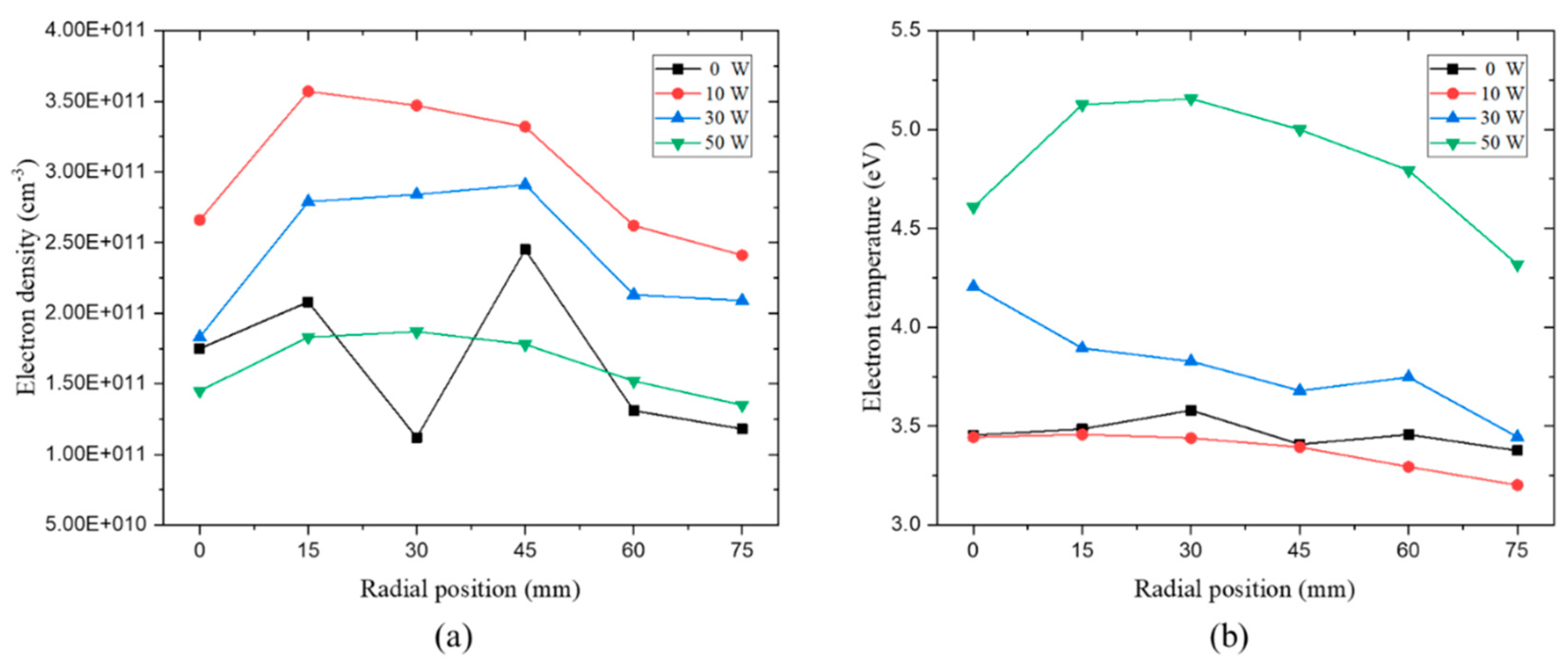
Figure 7 shows the electron temperature and electron density values at radial positions obtained by SLP due to bias power variation at 30 mTorr. In our experiment, the source power value was always in inductive mode (H-mode). Therefore, with the increase in bias power, the electron density value decreases and the electron temperature value increases [
37].
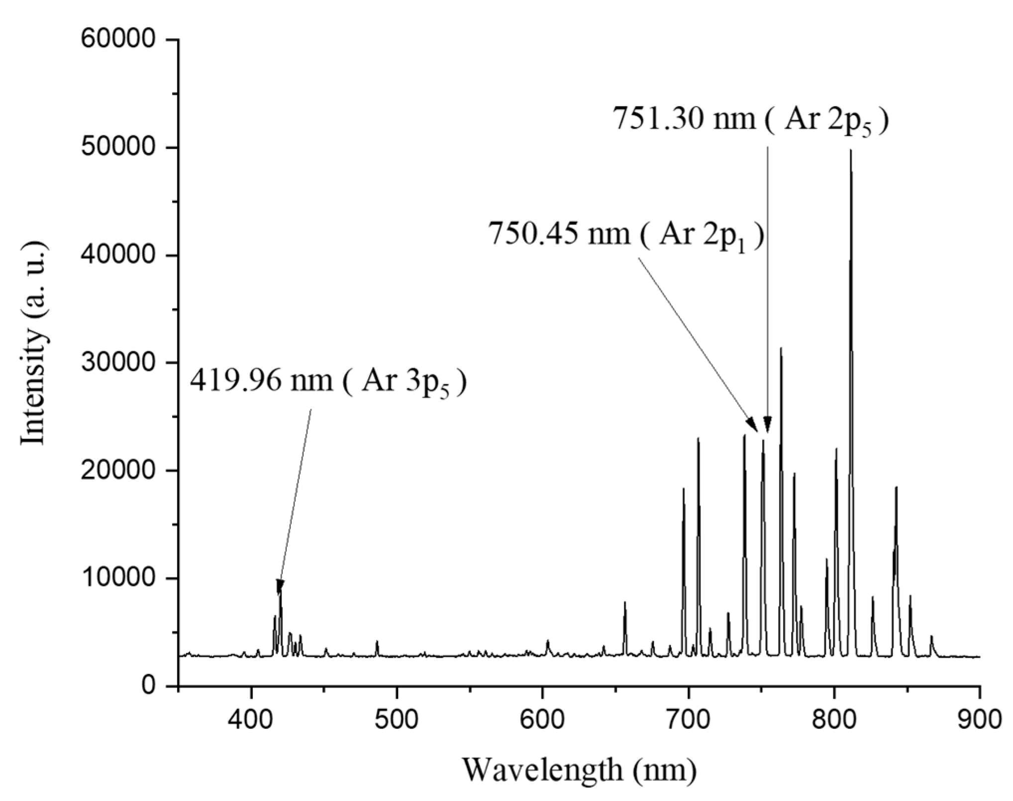
A wavelength selection experiment was conducted to use the line-ratio method of OES. Through the OES data as shown in
Figure 8, the intensity value of the Ar wavelength was compared by referring to the reference [
33], and peak with a constant tendency according to the parameter change was confirmed. Three peaks at 751.5 nm, 750.4 nm, and 419.8 nm were selected and then used to derive electron density and electron temperature. In general, there is a difference between the plasma parameter obtained through OES data and the SLP data [
38].
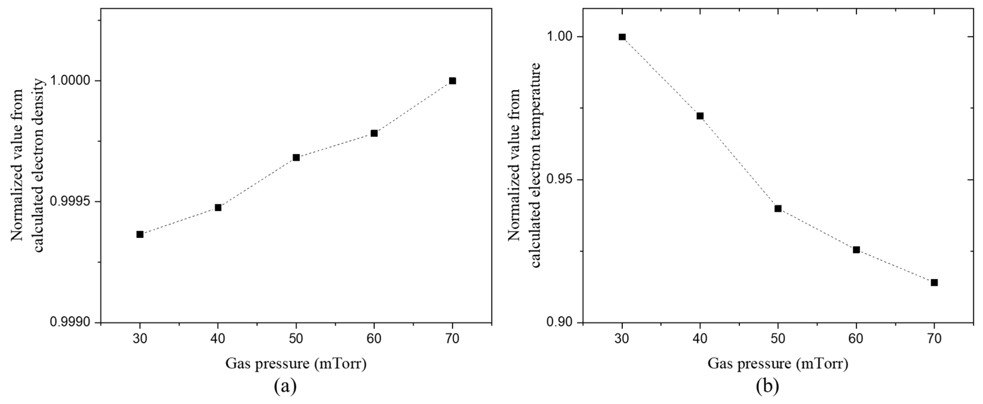
Figure 9 shows the normalization of the plasma parameter that was calculated using Eqn. 16. Although this obtained value is different from the experimental value, the result of normalization is significant with the tendency of the experimental value in the case of electron density. However, in the case of electron temperature, the value in the radial position tends to increase with the increase in pressure, in contrast to the trend that typically appears. As a result, the plasma parameter calculated as OES is differed to the SLP data value but like the tendency. Additionally, the plasma parameter cannot be derived according to the variation in bias power through OES. As the bias power varied, the intensity value of a particular Ar peak remained constant and was identical to the intensity value calculated using corresponding pressure. Therefore, bias power cannot affect the intensity value because it is not the main factor for direct plasma generation. The electron density can be altered depending on the radial position by bias power that affects bulk plasma uniformity. In addition, the difference in potential affects the main parameters of WIP temperature, such as ion energy, so the effect of bias power must be considered [
39]. Thus, ETSW is used to determine heat flux based on the variation in bias power.
4.2. Heat Flux Calculation
Table 2 shows the energy influx calculation results obtained by applying electron density and electron temperature obtained by the measured SLP data to Eqn. (12). Our results showed that energy influx has a tendency to increase with the radial position as the pressure increases. In addition, the energy flux at the edge is lower than the value at other radial positions. When the pressure in the ICP etcher is 30 mTorr, the energy influx was found to be 5580.8 W/m2, 7255.0 W/m2, 8851.9 W/m2, and 10179.4 W/m2 at the source power of 300 W, 400 W, 500 W, and 600 W, respectively [
32]. The energy influx value of the center, 4908.1 W/m2, showed a similar tendency under the conditions of 30 mTorr and 200 W.
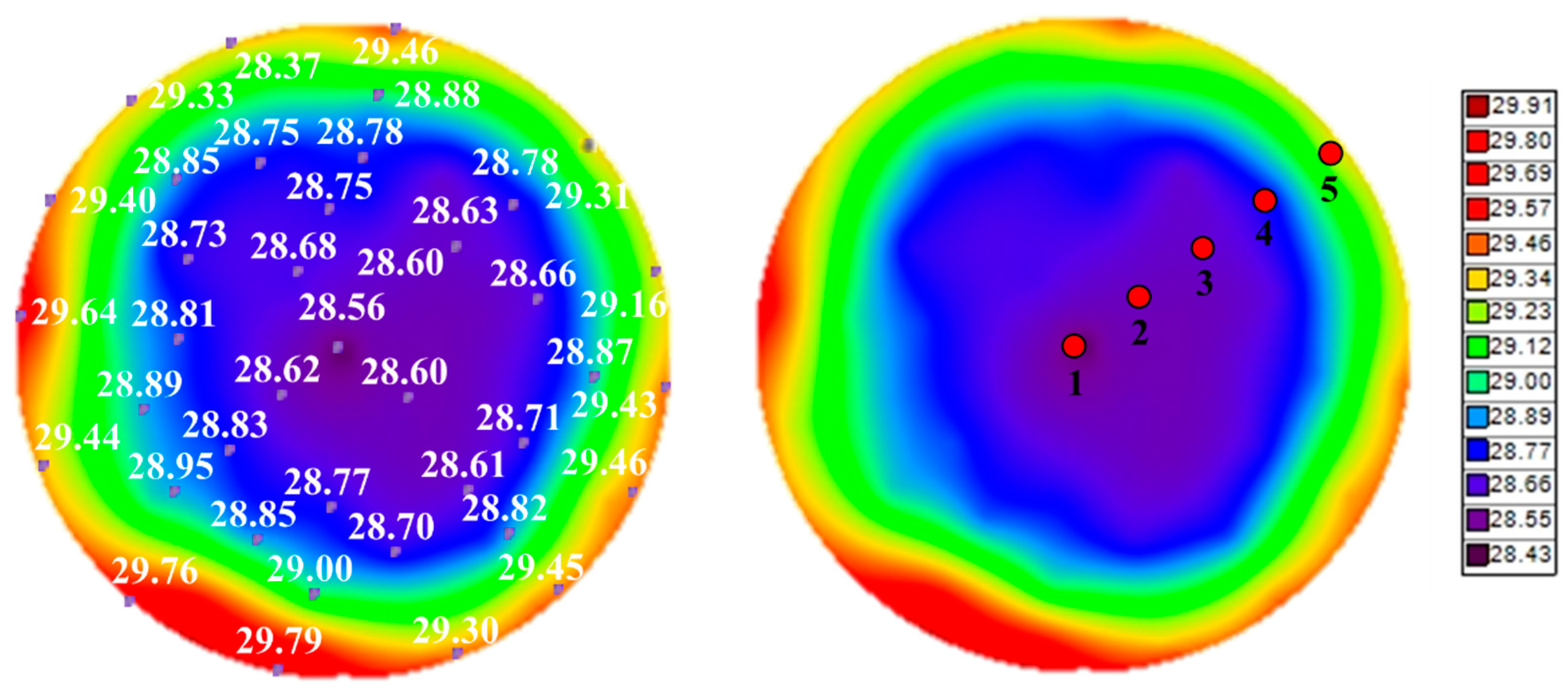
The energy influx value was derived by applying the ETSW data to Eqn. (1). The OES data was used to derive the plasma parameter in a 12-inch environment through the line-ratio method. The energy influx value according to the radial position was derived by applying the SLP data obtained at 6 inches. We measured the increase in plasma energy influx due to bias power using a wafer-type temperature sensor because there were limitations in using OES to extract plasma parameters with respect to changes in bias power. However, five of the 65 sensors were used, as shown in
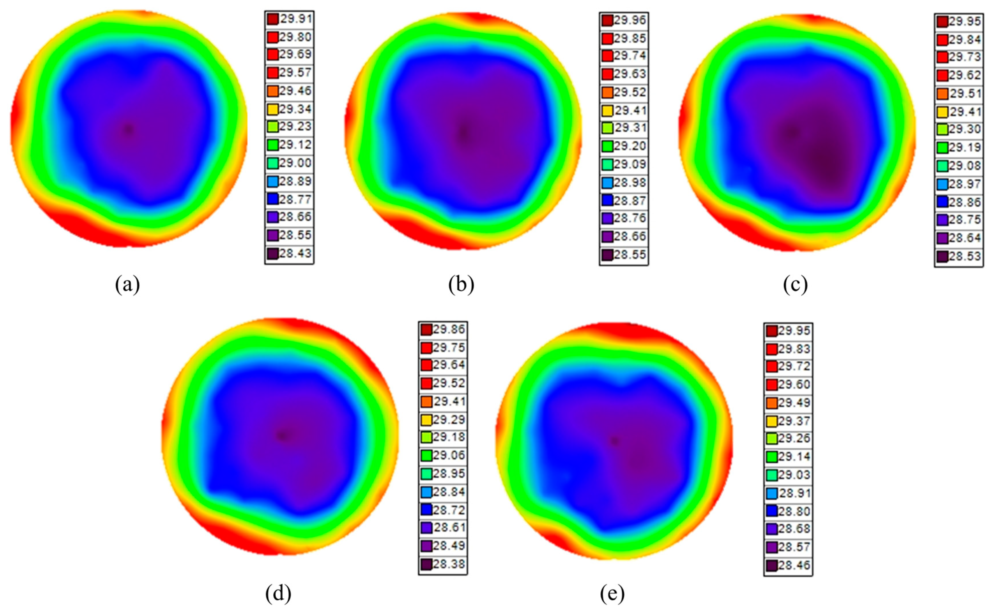
Figure 10, since the 12-inch radial position differs from the existing 6-inch radial position depending on the ETSW sensor position. The temperature sensor data was used at 0 mm, 37 mm, 74 mm, 110 mm, and 147 mm positions. The ETSW temperature uniformity data by pressure variation is shown in
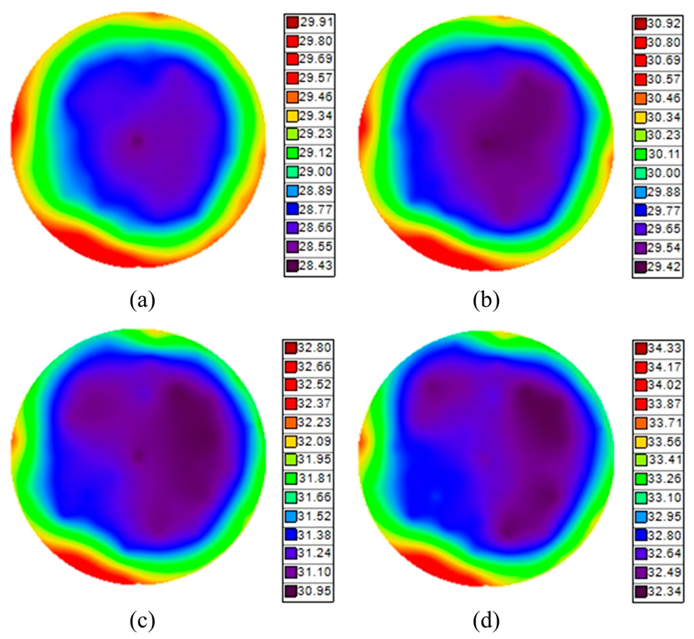
Figure 11, and the temperature data by bias variation is shown in
Figure 12.
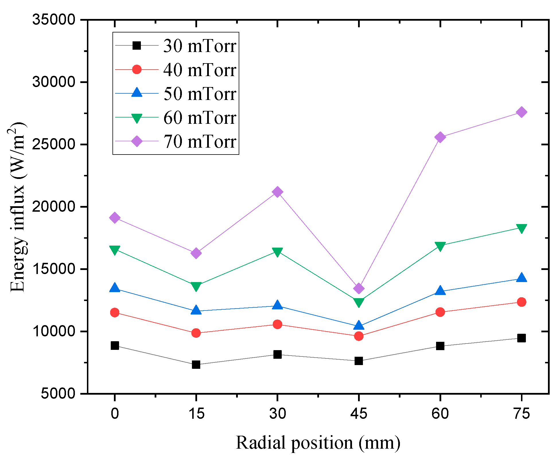
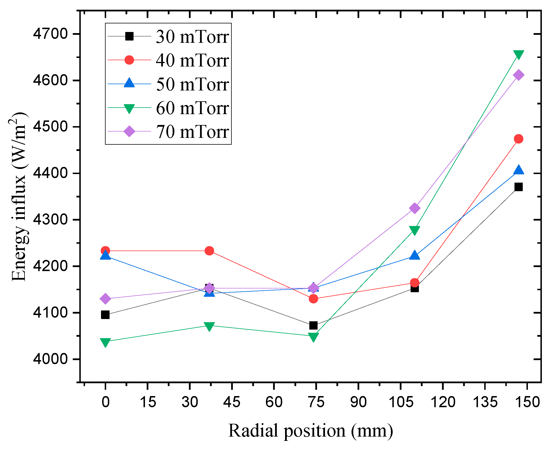
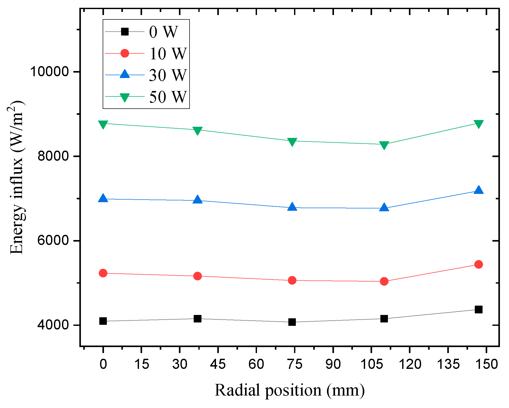
Figure 13 shows the pressure variation energy influx derived from OES data equipped with 12 inches without applying bias power. Pressure and bias power variation energy influx with Eqn. (1) applied in ETSW data is shown in
Figure 14 and
Figure 15.
4.3. Discussion
The electron density in the experiment shows a similar tendency. The tendency of electron density according to radial position is similar, and the difference lies only in the tendency of density to increase as pressure increases. When comparing the electron density tendency at lower pressure of 3 mTorr and higher pressure of 150 mTorr beyond the experimental pressure range, the experiment in the paper shows an intermediate tendency [
40]. The main cause of this difference is the electron energy relaxation length and the variation in electron heating mechanism. At high pressures, collisional heating dominates and heated electrons near the plasma boundary lose energy through inelastic and e–e collisions in the skin layer before reaching the plasma bulk. Therefore, the RF power is mainly deposited in the skin layer near the plasma boundary, and the maximum plasma density occurs at the chamber boundary. However, at low pressures, non-local electron kinetics can explain the different tendency. Electrons heated by the vortex electric field can pass through the skin layer in a short time and acquire net energy. They then traverse the entire volume before losing energy. Additionally, due to ambipolar diffusion, the maximum plasma potential exists at the center of the discharge chamber, leading to maximum kinetic energy for electrons at the center. As a result, the region of maximum ionization occurs near the center of the chamber, where there is absent or weak RF field.
The electron temperature in the experiment shows a tendency to increase and then decrease once at the 15mm position, except for the case of 30mTorr. This difference is likely due to the variation in coil shape. Additionally, when comparing simulations and experiments with the same coil shape as the actual experiment, differences in plasma potential distribution or electron temperature distribution can be observed [
41]. Therefore, since the variation in coil shape directly affects the shape of the plasma source region.
One of the plasma diagnostic sensors, OES, had limitations in measuring plasma parameters due to bias power variation among process parameters. Therefore, to derive plasma energy influx through OES, it is necessary to complement plasma parameters according to bias power variation using other diagnostic sensors. Energy influx values derived from 12-inch equipment using measurement sensors are at least twice as large as energy influx values derived from ETSW data and differ by up to five times. This is because the wafer-temperature decreases due to the cooling effect of the ESC backside gas, which results in a difference between the energy influx value calculated in plasma bulk and the energy influx value calculated in ETSW. Additionally, there was a difference in the value of the bulk plasma parameter obtained by each measurement sensor. As a result, a difference in energy influx values was observed. The energy influx derived from the 6-inch equipment tends to gradually decrease towards the edge, while the ETSW energy influx tends to increase as it goes towards the edge. The wafer-temperature in the wafer edge region can be increased by plasma and focus ring [
42]. As a result, the ETSW sensor temperature increases further in the edge region than in the center region. In addition, the temperature difference increases, leading to the higher value of energy influx in the edge than in the center region. Thus, the increases in bias power and energy influx are similar for each radial position. Energy influx with center-to-edge bias power variation also exhibits a similar tendency.
Figure 12 shows that wafer-temperature uniformity improves as bias power increases under the same conditions.
5. Conclusion
In this paper, we calculated energy influx with a radial position considering plasma characteristics using SLP, OES and ETSW sensors. In a 6-inch experimental environment, plasma parameters were derived and compared from the intensity ratio of a specific peak of OES and SLP by process parameter variation, and energy influx was derived from the equation. Energy influx values derived using measurement sensors and ETSW sensors with 12-inch production equipment were compared with those fitted with 6-inch equipment. We found that the change in bias power has a greater impact on energy influx than chamber pressure although the wafer edge region showed some amount of mismatch of the energy influx trends and ETSW measurement. Finally, the bulk plasma diagnostic sensor had difficulty in calculating the exact heat flux by interpreting the actual behavior occurring on the wafer surface. In the future, considering peripherals, such as ESC and focus ring, and various assumptions, such as incident angle, the increase in energy influx caused by bias power will enable more accurate wafer-temperature prediction.
Author Contributions
Conceptualization and methodology, S.J.H. and S.I.C.; validation and formal analysis, investigation, data curation, S.I.C. and H.K.P.; writing—original draft preparation, S.I.C. and S.A.; writing—review and editing, S.J.H.; visualization, S.I.C.; supervision, S.J.H.; project administration, S.J.H.; funding acquisition, S.J.H. All authors have read and agreed to the published version of the manuscript.
Funding
This research was supported by R&D Program of “Development and demonstration of intelligent technology for semiconductor plasma processing equipment (GID: 1711121944)” through the Korea Institute of Fusion Energy (KFE) funded by the Government funds.
Institutional Review Board Statement
Not applicable.
Informed Consent Statement
Not applicable.
Data Availability Statement
Experimental data are available upon request.
Acknowledgments
Authors are grateful to staff of Semiconductor Process Diagnosis and Research Center (SPDRC) at Myongji University for their professional management of 300 mm wafer fabrication equipment.
Conflicts of Interest
The authors declare no conflict of interest.
References
- Wu, B.; Kumar, A.; Pamarthy, S. High aspect ratio silicon etch: A review. Journal of applied physics. 2010, 108, 051101. [Google Scholar] [CrossRef]
- Huang, S.; Shim, S.; Nam, S.K.; Kushner, M.J. Pattern dependent profile distortion during plasma etching of high aspect ratio features in SiO2. Journal of Vacuum Science & Technology A: Vacuum, Surfaces, and Films. 2020, 38, 023001. [Google Scholar]
- Wang, S.; Wendt, A.E. Control of ion energy distribution at substrates during plasma processing. J. Appl. Phys. 2000, 88, 643–646. [Google Scholar] [CrossRef]
- Ishikawa, K.; Karahashi, K.; Ishijima, T.; Cho, S.I.; Elliott, S.; Hausmann, D.; Mocuta, D.; Wilson, A.; Kinoshita, K. Progress in nanoscale dry processes for fabrication of high-aspect-ratio features: How can we control critical dimension uniformity at the bottom? Japanese Journal of Applied Physics. 2018, 57(6S2), 06JA01. [Google Scholar] [CrossRef]
- Kim, Y.; Kang, S.K.; Kim, S.D.; Kim, S.E. Wafer warpage analysis of stacked wafers for 3D integration. Microelectronic engineering. 2012, 89, 46–49. [Google Scholar] [CrossRef]
- Shirazi, A.; Varvani-Farahani, A.; Lu, H. An inverse analysis of warpage for trilayer thin-plate under thermal cycles. Materials & Design. 2010, 31, 4219–4228. [Google Scholar]
- Kanno, S.; Miya, G.; Tanaka, J.; Masuda, T.; Kuwahara, K.; Sakaguchi, M.; Makino, A.; Tsubone, T.; Fujii, T. Controlling gate-CD uniformity by means of a CD prediction model and wafer-temperature distribution control. Thin Solid Films. 2007, 515, 4941–4944. [Google Scholar] [CrossRef]
- Du, H.C.; Hong, S.J. Temperature analysis of electrostatic chuck for cryogenic etch equipment. Journal of the Semiconductor & Display Technology. 2021, 20, 19–24. [Google Scholar]
- Hsu, K.C.; Yang, J.Y.; Chen, J.Z.; Yu, Y. H.; Chen, Y.J. Modeling and simulation of heat transfer characteristics of 12-inch wafer on electrostatic chuck. In 2015 10th International Microsystems, Packaging, Assembly and Circuits Technology Conference (IMPACT). 304-307.
- Olson, K.A.; Kotecki, D.E.; Ricci, A.J.; Lassig, S.E.; Husain, A. Characterization, modeling, and design of an electrostatic chuck with improved wafer temperature uniformity. Review of scientific instruments. 1995, 66, 1108–1114. [Google Scholar] [CrossRef]
- Shan, H.; Pu, B.Y.; Gao, H.; Ke, K.H.; Lewis, J.; Welch, M.; Deshpandey, C. Process kit and wafer temperature effects on dielectric etch rate and uniformity of electrostatic chuck. Journal of Vacuum Science & Technology B: Microelectronics and Nanometer Structures Processing, Measurement, and Phenomena. 1996, 14, 521–526. [Google Scholar]
- Wright, D.R.; Hartman, D.C.; Sridharan, U.C.; Kent, M.; Jasinski, T.; Kang, S. Low temperature etch chuck: Modeling and experimental results of heat transfer and wafer temperature. Journal of Vacuum Science & Technology A: Vacuum, Surfaces, and Films. 1992, 10, 1065–1070. [Google Scholar]
- Cui, Y.; Jian, S.; Chen, C.; Lin, Y.; Su, Z.; Zhang, H.; Yuan, R.; Chen, Z.; Dong, Z.; Li, L. Uniformity improvement of deep silicon cavities fabricated by plasma etching with 12-inch wafer level. Journal of Micromechanics and Microengineering. 2019, 29, 105010. [Google Scholar] [CrossRef]
- Zhao, S. X.; Gao, F.; Wang, Y. N.; Bogaerts, A. Gas ratio effects on the Si etch rate and profile uniformity in an inductively coupled Ar/CF4 plasma. Plasma Sources Science and Technology. 2012, 22, 015017. [Google Scholar] [CrossRef]
- Burtsev, A.; Li, Y.X.; Zeijl, H.W.; Beenakker, C. I. M. An anisotropic U-shaped SF6-based plasma silicon trench etching investigation. Microelectronic engineering. 1998, 40, 85–97. [Google Scholar] [CrossRef]
- Rosli, S. A.; Aziz, A.A.; Hashim, M. R. ICP-RIE dry etching using Cl2-based on GaN. Sains Malaysiana. 2011, 40, 79–82. [Google Scholar]
- Oehrlein, G.S.; Kurogi, Y. Sidewall surface chemistry in directional etching processes. Materials Science and Engineering: R: Reports. 1998, 24, 153–183. [Google Scholar] [CrossRef]
- Dixit, P.; Miao, J. Effect of clamping ring materials and chuck temperature on the formation of silicon nanograss in deep RIE. Journal of The Electrochemical Society. 2006, 153, G771. [Google Scholar] [CrossRef]
- Kim, T.W.; Aydil, E.S. Effects of chamber wall conditions on Cl concentration and Si etch rate uniformity in plasma etching reactors. Journal of the Electrochemical Society. 2003, 150, G418. [Google Scholar] [CrossRef]
- Durandet, A.; Joubert, O.; Pelletier, J.; Pichot, M. Effects of ion bombardment and chemical reaction on wafer temperature during plasma etching. Journal of applied physics. 1990, 67, 3862–3866. [Google Scholar] [CrossRef]
- Shinoda, K.; Miyoshi, N.; Kobayashi, H.; Miura, M.; Kurihara, M.; Maeda, K.; Negishi, N.; Sonoda, Y.; Tanaka, M.; Yasui, N. Selective atomic-level etching using two heating procedures, infrared irradiation and ion bombardment, for next-generation semiconductor device manufacturing. J. Phys. D. 2017, 50, 194001. [Google Scholar] [CrossRef]
- Kersten, H.; Stoffels, E.; Stoffels, W.W.; Otte, M.; Csambal, C.; Deutsch, H.; Hippler, R. Energy influx from an rf plasma to a substrate during plasma processing. Journal of Applied Physics. 2000, 87, 3637–3645. [Google Scholar] [CrossRef]
- Tinck, S.; Boullart, W.; Bogaerts, A. Simulation of an Ar/Cl2 inductively coupled plasma: study of the effect of bias, power and pressure and comparison with experiments. Journal of Physics D: Applied Physics. 2008, 41, 065207. [Google Scholar] [CrossRef]
- Kim, J.H.; Cho, S.W.; Park, C.J.; Chae, H.; Kim, C.K. Angular dependences of SiO2 etch rates at different bias voltages in CF4, C2F6, and C4F8 plasmas. Thin Solid Films. 2017, 637, 43–48. [Google Scholar] [CrossRef]
- Tandou, T.; Kubo, S.; Negishi, N.; Izawa, M. Improving the etching performance of high-aspect-ratio contacts by wafer temperature control: Uniform temperature design and etching rate enhancement. Precision Engineering. 2016, 44, 87–92. [Google Scholar] [CrossRef]
- Tinck, S.; Tillocher, T.; Dussart, R.; Bogaerts, A. Cryogenic etching of silicon with SF6 inductively coupled plasmas: a combined modelling and experimental study. Journal of Physics D: Applied Physics. 2015, 48, 155204. [Google Scholar] [CrossRef]
- Durandet, A.; Joubert, O.; Pelletier, J.; Pichot, M. Effects of ion bombardment and chemical reaction on wafer temperature during plasma etching. Journal of applied physics. 1990, 67, 3862–3866. [Google Scholar] [CrossRef]
- Freed, M.; Kruger, M.V.P.; Poolla, K.; Spanos, C.J. Wafer-grown heat flux sensor arrays for plasma etch processes. IEEE transactions on semiconductor manufacturing. 2005, 18, 148–162. [Google Scholar] [CrossRef]
- Lim, Y.M.; Eo, H.; Kim, K.H.; Lee, M.Y.; Chung, C.W. A wafer-like apparatus for two-dimensional measurement of plasma parameters and temperature distribution in low-temperature plasmas. Review of Scientific Instruments. 2021, 92, 053531. [Google Scholar] [CrossRef]
- Kersten, H.; Snijkers, R.J.M.M.; Schulze, J.; Kroesen, G.M.W.; Deutsch, H.; De Hoog, F.J. Energy transfer from radio frequency sheath accelerated CF+ 3 and Ar+ ions to a Si wafer. Applied physics letters. 1994, 64, 1496–1498. [Google Scholar] [CrossRef]
- Shindo, W.; Ohmi, T. Ion energy, ion flux, and ion mass effects on low-temperature silicon epitaxy using low-energy ion bombardment process. Journal of applied physics. 1996, 79, 2347–2351. [Google Scholar] [CrossRef]
- Lim, Y.D.; Lee, D.Y.; Yoo, W.J.; Ko, H.S.; Lee, S.H. Temperature of a semiconducting substrate exposed to an inductively coupled plasma. Journal of the Korean Physical Society. 2011, 59, 262–270. [Google Scholar] [CrossRef]
- Zhu, X.M.; Pu, Y.K. A simple collisional–radiative model for low-pressure argon discharges. Journal of Physics D: Applied Physics, 2007, 40, 2533. [Google Scholar] [CrossRef]
- Zhu, X.M.; Chen, W.C.; Li, J.; Pu, Y.K. Determining the electron temperature and the electron density by a simple collisional–radiative model of argon and xenon in low-pressure discharges. Journal of Physics D: Applied Physics. 2008, 42, 025203. [Google Scholar] [CrossRef]
- Gao, F.; Zhao, S.X.; Li, X.S.; Wang, Y.N. Comparison between experiment and simulation for argon inductively coupled plasma. Physics of Plasmas 2009, 16, 113502. [Google Scholar] [CrossRef]
- Okada, K.; Komatsu, S.; Matsumoto, S. Langmuir probe measurements in a low pressure inductively coupled plasma used for diamond deposition. Journal of Vacuum Science & Technology A: Vacuum, Surfaces, and Films. 1999, 17, 721–725. [Google Scholar]
- Lee, H.C.; Lee, M.H.; Chung, C.W. Effects of rf-bias power on plasma parameters in a low gas pressure inductively coupled plasma. Applied Physics Letters. 2010, 96, 071501. [Google Scholar] [CrossRef]
- Park, H.; Choe, W. Parametric study on excitation temperature and electron temperature in low pressure plasmas. Current Applied Physics, 2010, 10, 1456–1460. [Google Scholar] [CrossRef]
- Wang, S.Q.; Macdonald, P.; Kruger, M. Plasma etch process diagnosis and control by wireless sensor wafer in semiconductor chip manufacturing. In 2006 8th International Conference on Solid-State and Integrated Circuit Technology Proceedings 2006. IEEE, 2006, 2175-2180.
- Yue, H.U.A.; Jian, S.O.N.G.; Zeyu, H.A.O.; Zhang, G.; Chunsheng, R.E.N. Effects of direct current discharge on the spatial distribution of cylindrical inductively-coupled plasma at different gas pressures. Plasma Science and Technology. 2017, 20, 014005. [Google Scholar]
- Collison, W.Z.; Ni, T.Q.; Barnes, M.S. Studies of the low-pressure inductively-coupled plasma etching for a larger area wafer using plasma modeling and Langmuir probe. Journal of Vacuum Science & Technology A: Vacuum, Surfaces, and Films. 1998, 16, 100–107. [Google Scholar]
- Suzuki, A.; Terasawa, N.; Moriya, T.; Kang, S.Y. Effects of surface conditions of the focus ring on etching uniformity. In 2010 International Symposium on Semiconductor Manufacturing (ISSM), 2010, 1-3.
|
Disclaimer/Publisher’s Note: The statements, opinions and data contained in all publications are solely those of the individual author(s) and contributor(s) and not of MDPI and/or the editor(s). MDPI and/or the editor(s) disclaim responsibility for any injury to people or property resulting from any ideas, methods, instructions or products referred to in the content. |
© 2023 by the authors. Licensee MDPI, Basel, Switzerland. This article is an open access article distributed under the terms and conditions of the Creative Commons Attribution (CC BY) license (http://creativecommons.org/licenses/by/4.0/).
