1. Introduction
Group-IV GeSn material system is under extensive development for low-cost and high-performance infrared (IR) photodetectors (PDs) because of the unique advantage of complementary metal-oxide-semiconductor (CMOS) compatibility for a wide spectrum of applications covering military, communication, and thermal vision [
1,
2]. GeSn alloys offer a wide range of bandgap tunability by adjusting the Sn composition [
3,
4], thereby permitting expansion of their direct-gap absorption edge from ~1500 nm to short-wave IR (SWIR) range (1.5-3 μm), mid-wave infrared (MWIR) range (3–8 μm), and even long-wave infrared (LWIR) (8–14 μm). In addition, the presence of the indirect conduction band enables a unique momentum-space carrier separation scheme to enable high-performance photodetection [
5,
6]. Most importantly, GeSn PDs can be monolithically integrated with electronics on the same Si or silicon-on-insulator (SOI) chip for seamlessly manufacturing in modern CMOS foundries, allowing for the development of low-cost, high-performance, complex, and functional image systems [
7,
8] for a wide range of applications. These unique advantages have encouraged the development of various types of GeSn PDs [
8,
9,
10,
11,
12,
13,
14,
15,
16,
17,
18,
19,
20,
21,
22,
23,
24,
25] with remarkable photodetection range up to 4600 nm [
25]. More recently, a comprehensive theoretical study of GeSn PDs has indicated that the performance of GeSn PDs when reaching material maturity is comparable with, and even better than, market-dominated IR PDs [
6], showing great promises for low-cost and high-performance IR detection.
IR PDs usually require cryogenic cooling to suppress dark current in order to reach high performance for practical photodetection. In addition, the device performance such as dark current, cutoff wavelength, responsivity, and detectivity are strongly dependent on the operation temperature as well as alloy composition. Thus, from the viewpoint of device and system developers, a rule of thumb is extremely useful to describe the performance of IR photodetectors in terms of operation temperature and alloy composition to achieve desired performance for meeting the requirement of various applications. Such simple relationships have been established to evaluate the performance of IR PDs including Mercury-Cadmium-Telluride (MCT) PDs (rule-07) [
26] and extended-wavelength InGaAs PDs (IGA-rule-17) [
27]. However, such a simple rule of thumb has not been developed for GeSn PDs so far. Here, for the first time, a heuristic rule is proposed and established for GeSn PDs with various Sn compositions and operation temperatures as GeSn-rule 23, where the prefix GeSn stands for GeSn PDs and the postfix 23 represents the year 2023, to evaluate the performance of GeSn PDs for the device and system developers to advance the GeSn IR PD technology.
The rest of the paper is organized as follows: the structure of the GeSn
p-i-n PD under investigation is described in
Section 2; the theoretical models of temperature-dependent bandgap energies for analyzing the cutoff wavelength in terms of Sn composition and operation temperature are presented in section 3; the theoretical models for evaluating dark current density and the establishment of GeSn-rule-23 are presented in section 4; the theoretical models of temperature-dependent absorption coefficient and optical responsivity are shown in section 5; the detectivity and noise-equivalent power in terms of Sn content and operation temperature are discussed in section 6; the analysis of temperature-dependent bandwidth of GeSn PDs is given in section 7; and finally the conclusion is summarized in
Section 8.
2. GeSn Device Structure
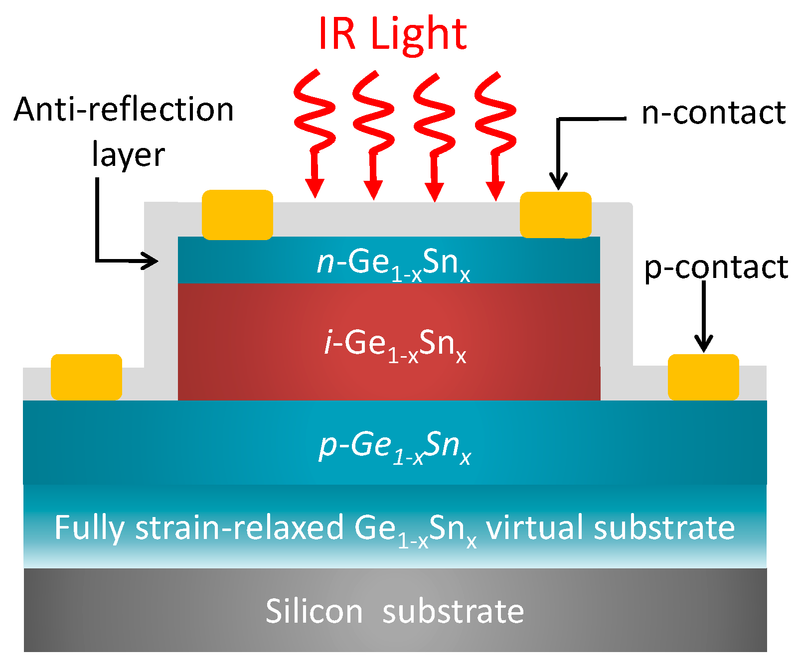
To establish the GeSn PDs’ fundamental performance, here we shall consider a general normal-incidence Ge
1-xSn
x p-i-n homojunction PDs with a circular mesa, as shown in
Figure 1. The Ge
1-xSn
x p-i-n diode is grown on a (001) silicon substrate via a fully strain-relaxed Ge
1-xSn
x virtual substrate (VS), so the entire Ge
1-xSn
x p-i-n stack is strain-free. The intrinsic Ge
1-xSn
x layer can convert the incident IR photons to electron-hole pairs via optical absorption, which are then swept to across the
p-i-n junction and collected as electrical currents. To achieve high responsivity and suppress tunneling dark current, a thick intrinsic Ge
1-xSn
x layer is necessary. Here, we set the thickness of the intrinsic Ge
1-xSn
x layer to be
ti=3000 nm. The thickness of the
n- Ge
1-xSn
x and
p- Ge
1-xSn
x are fixed to
tn=100 nm and
tp=500 nm, respectively. The doping concentrations in the
n-Ge
1-xSn
x and
p-Ge
1-xSn
x are set to
and
respectively. We make several assumptions in order to evaluate their achievable performance. First, we shall assume that the entire Ge
1-xSn
x p-i-n stack is defect-free as the defects can be properly confined in the Ge
1-xSn
x VS [
8]. The diameter of the GeSn diode mesa is set to
D=50 µm, which is significantly larger than the wavelength of interest so the diffraction effect is negligible. On the top of the GeSn is an antireflection layer which can minimize the reflection loss and thereby enhance quantum efficiency. The parameters for GeSn alloys used in this study were obtained from linear interpolation between these of Ge and α-Sn [
28].
3. Temperature Dependent Bandgap Energies and Cutoff Wavelength
The cutoff wavelength (
λc) of the Ge
1-xSn
x PDs is determined by optical absorption edges of the
i- Ge
1-xSn
x active layer. For Ge
1-xSn
x alloys, the optical absorption has two contributors, the direct-gap and indirect-gap interband absorption, owing to the proximity of the Γ- and L-valley conduction band (CB). However, the indirect-gap interband absorption is much weaker than the direct-gap one [
6] because of the need of additional phonons for momentum conservation. As a result, the cutoff wavelength of the Ge
1-xSn
x PDs is dominated by the direct-bandgap (
) via the expression
. The temperature- and composition-dependent direct bandgap energy of Ge
1-xSn
x alloys can be calculated using the Varshni equation [
29,
30,
31]
where
α and
β are the Varshni parameters for Ge
1-xSn
x alloys,
is the Γ-valley bandgap energy at T=0 K, and
is the bowing parameter [
29]. The Varshni parameters for Ge
1-xSn
x alloys are obtained by linear interpolation from these of Ge and α-Sn given in
Table 1.
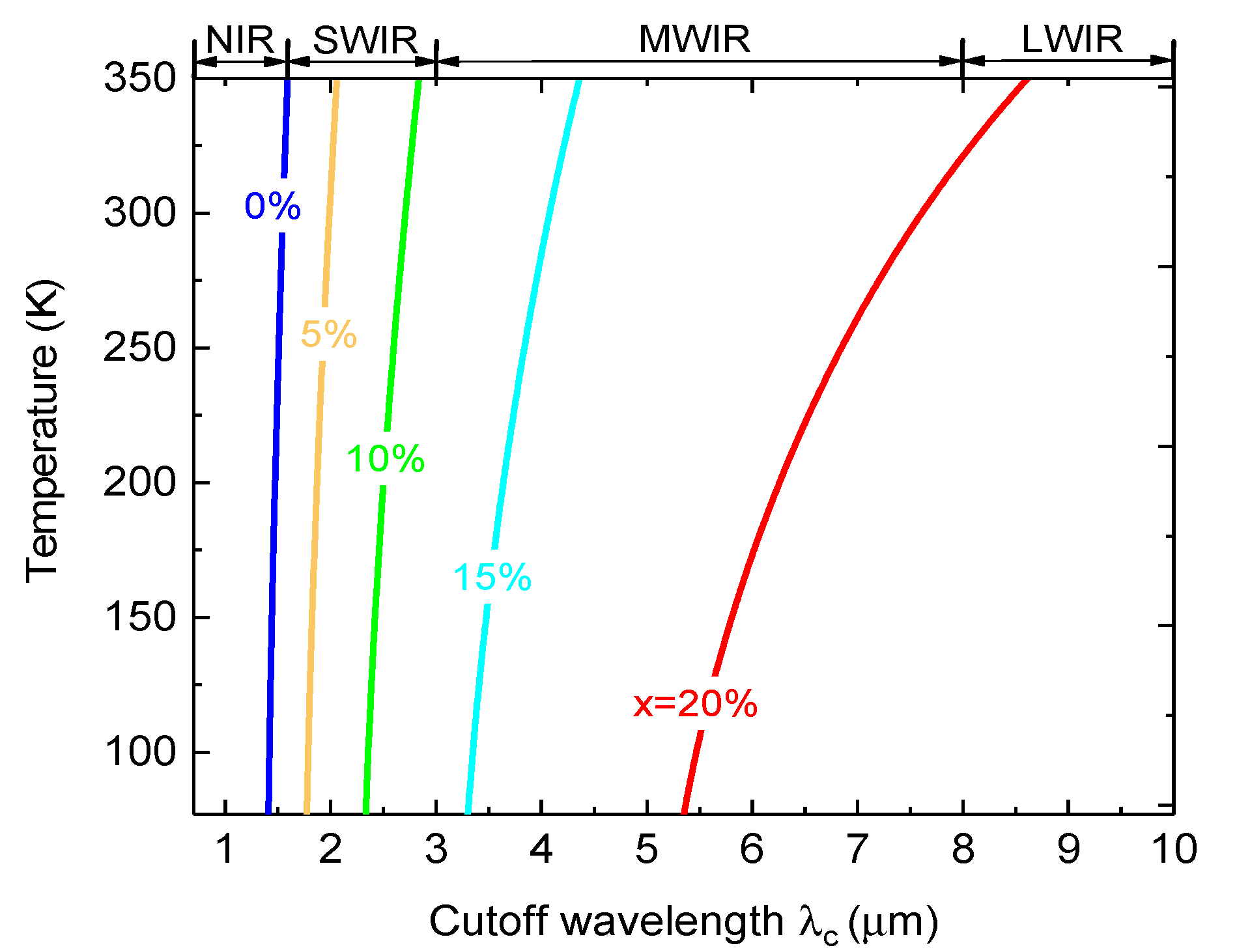
The relationship between the operation temperature and cutoff wavelength for GeSn PDs with different Sn compositions are shown in
Figure 2. For a fixed Sn content, the cutoff wavelength increases with increasing temperature. For pure Ge (x=0%), the cutoff wavelength can only reach NIR. As the Sn content increases, the cutoff wavelength of Ge
1-xSn
x PDs significantly redshifts attributed to the bandgap shrinkage owing to the incorporation of Sn, and can reach SWIR, MWIR, and even LWIR range with a sufficiently high Sn content. These results show that Ge
1-xSn
x PDs can operate in different IR spectral ranges by adjusting the Sn content for different applications.
4. Dark Current Density and GeSn-Rule 23
For defect-free Ge
1-xSn
x PDs, the dark current density is dominated by minority carrier diffusion currents [
6]. The diffusion dark current density at zero bias under short-base approximation can be calculated using [
6]
where
q is the elementary charge,
,
, and
are the diffusion coefficients for holes, and electrons in the Γ-CB and L-CB, respectively;
is the minority hole density in the
n-GeSn region,
and
are the minority electron densities in the Γ- and L-CB in the
p-GeSn region, The diffusion coefficient can be converted from mobility (
µ) via the Einstein relationship via
D=µkT/q with
k being the Boltzmann constant [
31]. The minority carrier concentrations in the doped layers can be linked to the intrinsic carrier concentrations and doping concentrations via
and
. The intrinsic carrier concentration (
ni) in GeSn alloys can be calculated using [
6,
31]
where
is the reduced Planck constant,
and
are the electron effective masses in the Γ- and L-CB, respectively,
is the hole effective mass in the valence band, which are taken from a 30-band full-zone k·p model [
32]. The electron mobility in the Γ-CB (
) and L-CB (
) and the hole mobility (
) (in units of cm
2V
-1s
-1) for intrinsic Ge
1-xSn
x at T=300 K can be expressed as [
34,
35]
The temperature-dependent mobility can be approximated with the power law
[
35], where
p is a constant. Owing to the lack of experimental data for GeSn alloys, the coefficients are approximated by these of Ge (
p=1.66 for electrons and
p=2.33 for holes [
35].) With the mobilities, the minority mobility can be estimated using [
36,
37]
where
Na and
Nd are the doping concentrations (in units of cm
-3) in the
p- and
n-GeSn regions, respectively. With the dark current density, the
R0A product can be obtained using [
31]
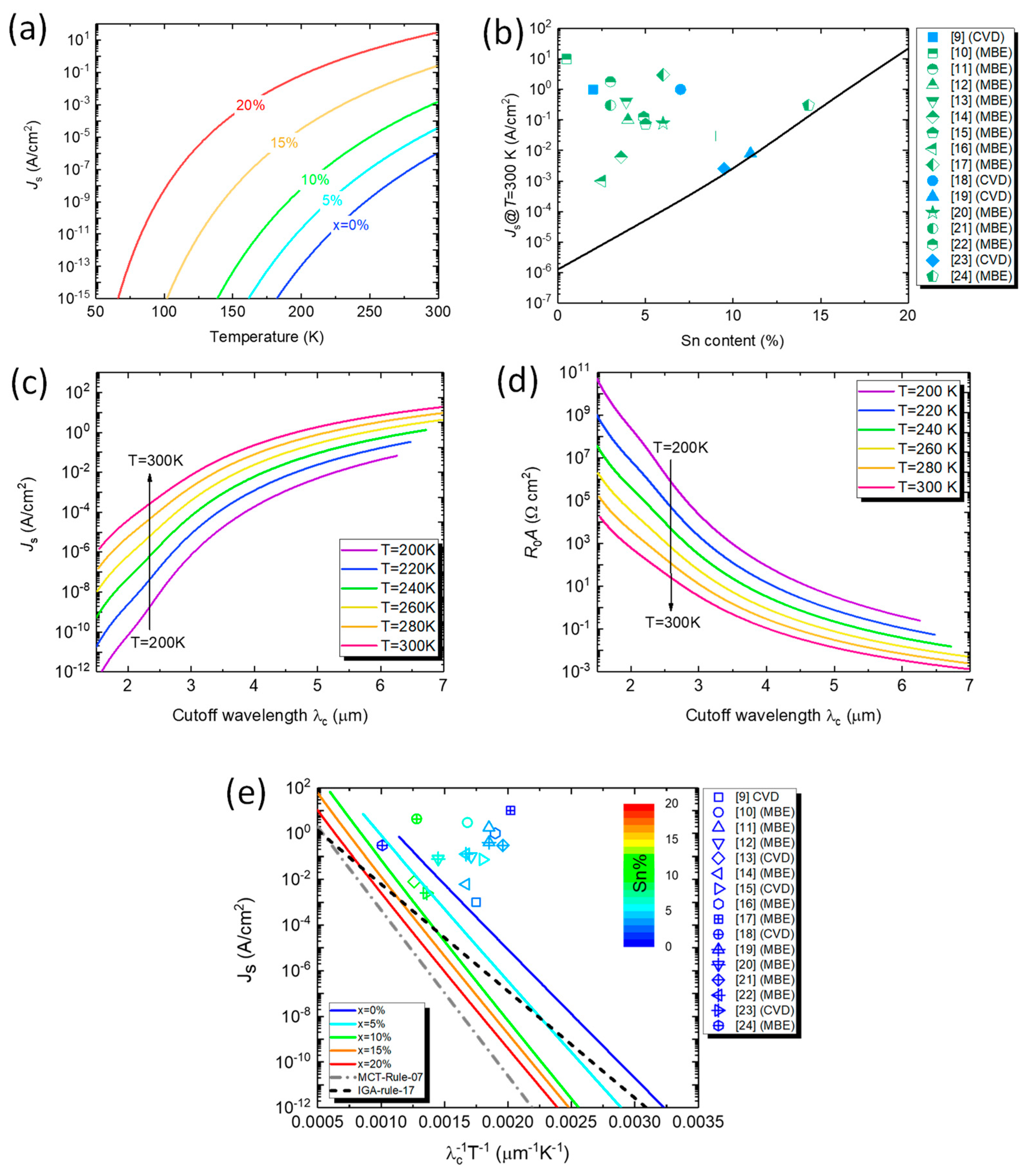
Figure 3a shows the calculated dark current density as a function of operation temperature for Ge
1-xSn
x PDs with different Sn compositions. For a fixed Sn content, the dark current increases with increasing temperature owing to higher intrinsic carrier concentration. In addition, the dark current density also increases with increasing Sn content owing to higher intrinsic carrier concentration as a result of reduced bandgap energy.
Figure 3b shows the calculated dark current density compared with selected experimental data from the reported Ge
1-xSn
x PDs operated at -1V bias voltage and
T=300 K [
9,
10,
11,
12,
13,
14,
15,
16,
17,
18,
19,
20,
21,
22,
23,
24]. It can be found that the calculated dark current density is generally 2-3 orders of magnitude smaller than experimental data at
T=300K. The results suggest that it is possible to significantly improve the dark current density by continuously improving the material quality.
Figure 3c,d show the calculated dark current density and
R0A product as a function of cutoff wavelength at various temperatures in the range of
T=200-300 K, respectively. At a fixed temperature, Ge
1-xSn
x PDs require a higher Sn composition to extend the cutoff wavelength, causing larger dark current density and smaller
R0A. At higher temperatures, the dark current density goes up while
R0A product goes down.
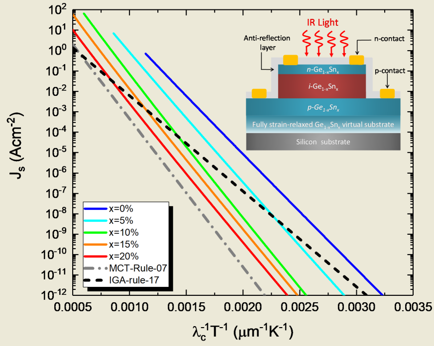
Figure 3e depicts the calculated dark current density as a function of product reciprocal of the product cutoff wavelength and temperature product (
λcT)
-1 for Ge
1-xSn
x PDs with various Sn compositions. Also plotted in
Figure 3e are the selected experimental data from the reported Ge
1-xSn
x PDs operated at -1V bias voltage [
9,
10,
11,
12,
13,
14,
15,
16,
17,
18,
19,
20,
21,
22,
23,
24] as well as the MCT rule-07 [
26] and IGA-rule-17 [
27]. It can be seen that, for a fixed Sn composition, the dark current density decreases with increasing (
λcT)
-1 because lower temperatures suppress the dark current density. The experimental data observed in Ge
1-xSn
x PDs show dark current densities about 1~3 orders of magnitude higher than the calculated performance. This discrepancy is likely attributed to (1) the residual compressive strain in the Ge
1-xSn
x active layer that enlarges the bandgap energy and thus blueshifts the cutoff wavelength, and (2) the defects in the Ge
1-xSn
x active layer that induce defect-related dark currents. These results suggest that there is considerable room to reduce the dark current density of Ge
1-xSn
x PDs by improving the material quality. In comparison with IGA-rule-07, it is found that Ge
1-xSn
x PDs with low Sn compositions (<5%) have higher dark current density than the E-InGaAs PDs for small (
λcT)
-1. As the Sn composition increases, the dark current density decreases, and eventually becomes comparable to, or even lower than, the E-InGaAs PDs, suggesting superior performance can be obtained with Ge
1-xSn
x PDs operating in longer-wavelength and higher-temperature conditions. Relative to MCT-rule-07, however, the Ge
1-xSn
x PDs exhibit higher dark current densities than MCT PDs.
We now establish GeSn-rule-23 based on our calculation results. The relationship between the dark current density, cutoff wavelength, and operation temperature can be described by the empirical expression [
26,
27]
where
C’ and
J0 are the fitting parameters, which can be obtained using the calculated results in
Figure 3e and the results are listed in
Table 2. These results offer device and system developers to easily evaluate the performance of GeSn PDs at different operation conditions. The dark current density of Ge
1-xSn
x PDs at
T=300 K (
Js@
T=300K) are also listed in
Table 2 for comparison.
Js@
T=300K significantly increases with increasing Sn contents as a result of narrower bandgap energy.
5. Temperature-Dependence Optical Absorption and Responsivity
Next, we calculate the temperature-dependent optical absorption coefficient and responsivity of the GeSn PDs. For GeSn alloys, both direct-gap and indirect-gap interband transitions contribute to optical absorption. However, the indirect-gap interband transition is much weak than the indirect-gap because additional phonons are necessary to conserve momentum. Thus, the absorption coefficient is dominated by the direct-gap absorption coefficient. The direct-gap optical absorption coefficient by the direct-gap transitions can be calculated using the Fermi’s golden rule taking into account the Lorentzian lineshape function and the nonparabolicity effect as [
4]
where
nr is the refractive index of GeSn alloys;
c is the velocity of light in vacuum;
ɛ0 is the free space permittivity;
m0 is the rest mass of electron;
ω is the angular frequency of incident light;
E is the incident photon energy;
is the momentum matrix with
Ep denoting the optical energy parameter;
γ is the full-width-at-half-maximum (FWHM) of the Lorentzian lineshape function.
and
the electron energy in the Γ-CB and hole energy in the valence band, respectively, which are calculated using a multi-band k·p model presented in Refs. [
4,
38].
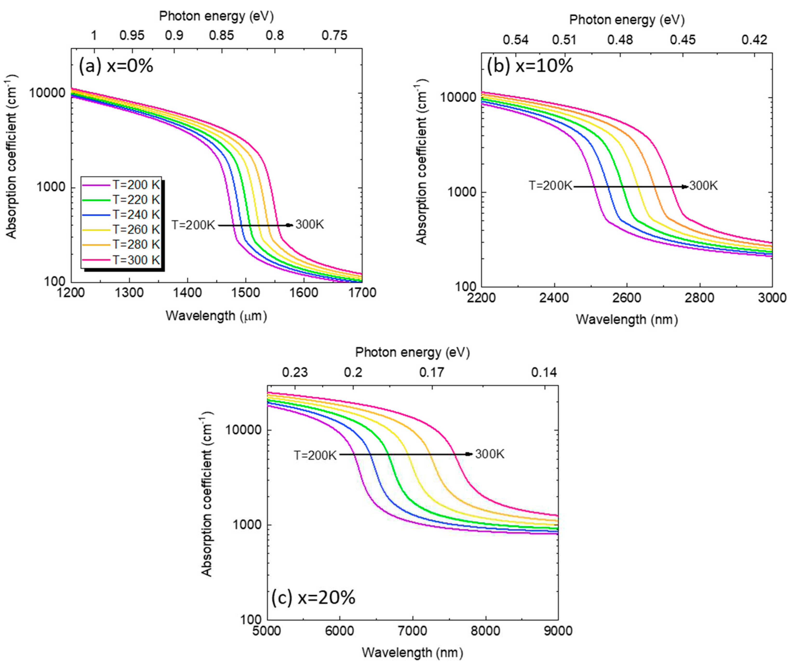
Figure 4 depicts the calculated absorption coefficient spectra of GeSn alloys with different Sn contents in the temperature range of
T=200-300 K. For a fixed Sn content and temperature, the absorption coefficient gradually decreases with increasing wavelength, followed by a sharp decrease near the direct-bandgap energy. It can also be observed that the absorption spectra redshift as the temperature increases because of the reduced direct bandgap energy. Note that the direct-gap absorption coefficient is related to the joint density-of-state (JDOS), which is proportional to
[
30]. As a result, the absorption coefficient at a fixed wavelength increases with increasing temperature. As the Sn content increases, the absorption coefficient significantly redshifts owing the narrowed bandgap energy caused by Sn alloying. As a result, the absorption coefficient in the MWIR region can be significantly enhanced, thereby enabling efficient MWIR photodetection.
With the absorption coefficient, we can then calculate the optical responsivity (
) of the GeSn PDs using [
30]
where
ηi is the internal quantum efficiency and its value is assume to be
ηi=100%; and
Rrefl is the reflectivity of the top surface of the GeSn PDs and its value is assumed to be zero as the anti-reflection coating can minimize the reflection.
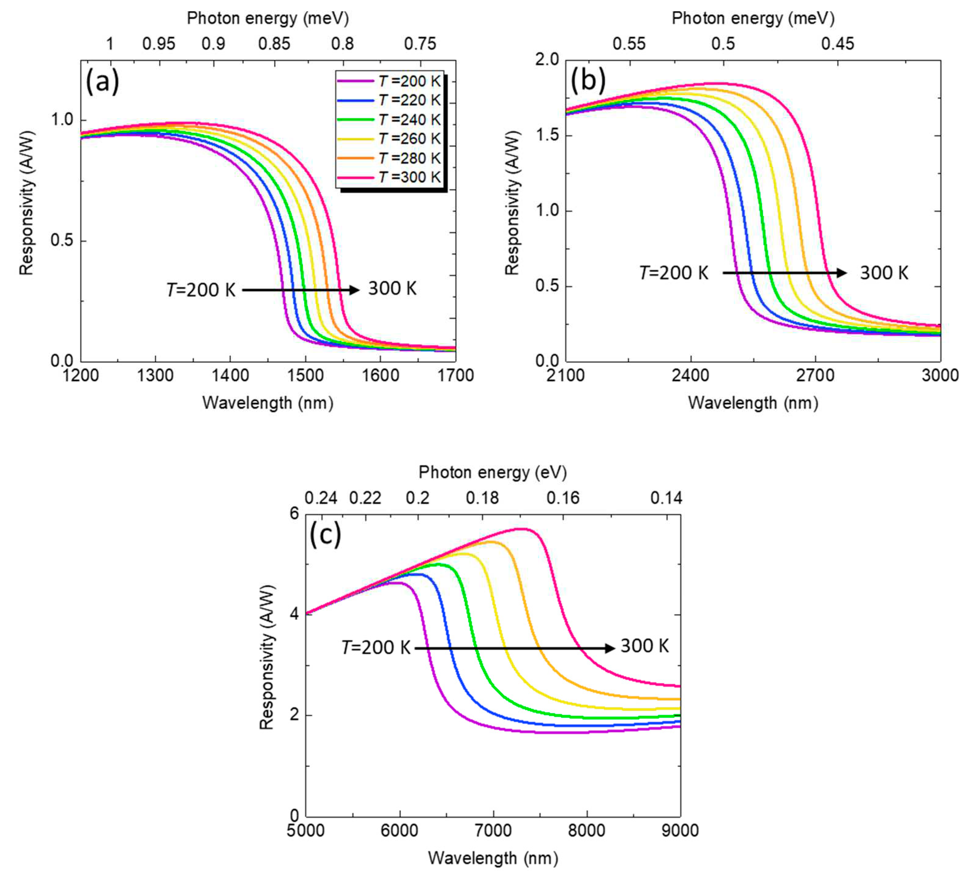
Figure 5 depicts the calculated optical responsivity spectra of the GeSn PDs with various Sn contents in the temperature range of
T=200-300 K. For pure Ge PDs (
x=0%), as shown in
Figure 5a, the responsivity increases with increasing wavelength, and then sharply decreases near the direct-gap absorption edge, correspondingly to the cutoff wavelength of the PD. With an increase in the operation temperature, the cutoff wavelength exhibits a redshift, indicating a wider photodetection range. As the Sn content increases to 10%, as shown in
Figure 5b, the cutoff wavelength is significantly extended to ~2600 nm. Meanwhile, the optical responsivity significantly increases because the reduced photon energy per photon leads to more photons for a watt of light energy. As the Sn content further increases to 20%, the cutoff wavelength is further extended to ~7000 nm with enhanced optical responsivity, enabling sensitive MWIR photodetection.
6. Temperature-Dependence Detectivity and Noise-Equivalent Power
The figure-of-merit for the performance of PDs includes not only dark current density, but also detectivity. Next, we calculate detectivity of Ge
1-xSn
x PDs in terms of Sn content and temperatures. With
R0A and responsivity
Rλ, we can obtain the specific detectivity (
), one the most important figure-of-merits used to characterize PDs’ performance, as [
6,
30]
The corresponding metric noise-equivalent power (NEP), which represents the minimum detectable power per square root bandwidth, can be computed as [
30]
where
A(=
) is the area of the photosensitive region of the GeSn PDs and is the bandwidth of the PD.
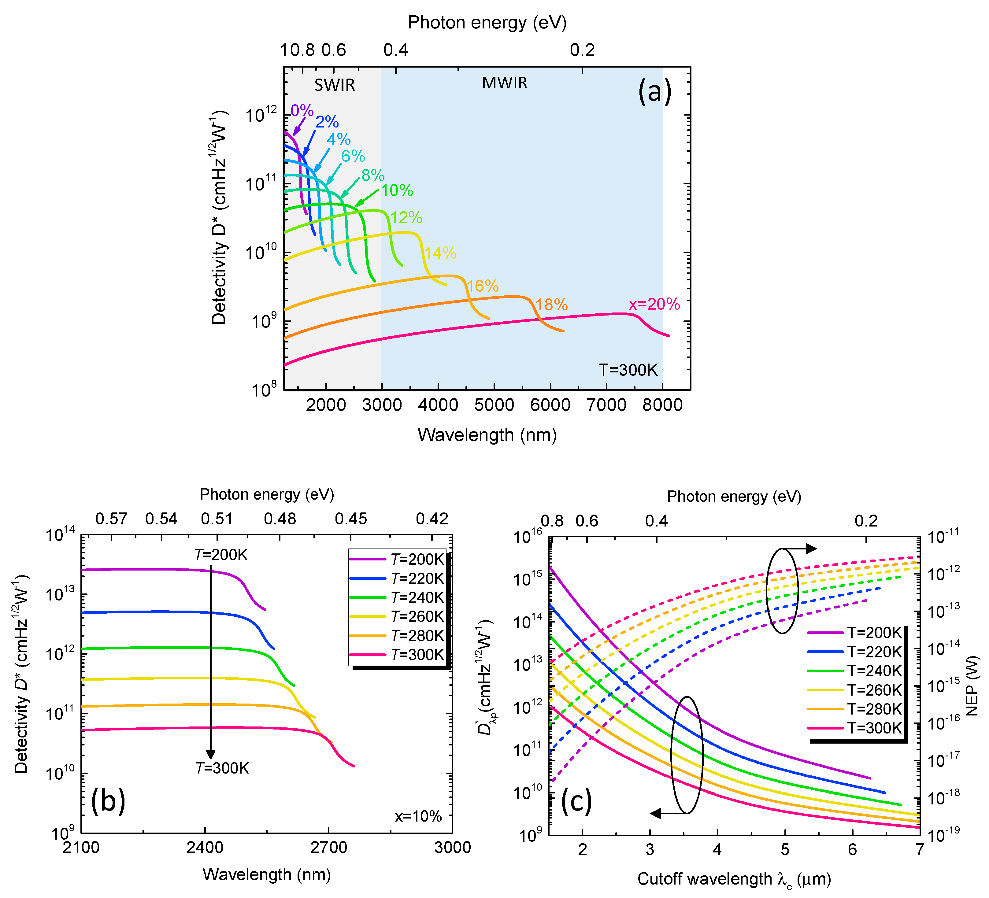
Figure 6a shows the calculated specific detectivity spectra of the GeSn PDs with various Sn content at
T=300K. For a fixed Sn content,
increases with increasing wavelength, followed by a rapid decrease near the direct-gap absorption edge. As a result, the peak detectivity (
) is obtained at a wavelength of about
. For
x=0, a high
is achieved at
λ~1500 nm. As the wavelength increase,
drops rapidly and becomes negligible near the direct-gap absorption edge because incident IR photons cannot be fully absorbed by the GeSn active region. As the Sn content increases, the detectivity spectrum is extended to longer wavelengths owing to the reduced direct bandgap, and can fully cover the entire SWIR (MWIR) spectral range with a Sn content of ~12% (~20%). However,
also decreases as a result of increased dark current density.
Figure 6b shows the calculated specific detectivity spectra for GeSn PDs with
x=10% in the temperature range of
T=200-300 K. As the temperature decreases,
significantly increases owing to the suppressed dark current density. Meanwhile, the photodetection range exhibits a blueshift as a result of increased direct bandgap energy. (For other Sn contents, similar results are obtained.)
Figure 6c shows the peak detectivity
(which is defined as the detectivity at the wavelength
) and the corresponding NEP normalized to a bandwidth of
as a function of cutoff wavelength in the temperature range of
T=200-300 K. At a fixed temperature,
decreases and NEP increases with increasing cutoff wavelength of the Ge
1-xSn
x PDs owing to higher Sn compositions. Meanwhile,
decreases and NEP increases at higher operation temperatures owing to increased dark current density.
7. Temperature-Dependence Bandwidth
We then investigate the temperature-dependent 3-dB bandwidth of the GeSn PDs. The 3-dB bandwidth of PDs are usually governed by transit-time delay and RC time delay. The transit-time delay limited bandwidth (
fT) can be calculated using [
39,
40]
where
vs is the carrier saturation velocity. The carrier saturation velocity at
T=300 K can be calculated using [
40,
41]
Where
,
cs is the velocity of sound in the GeSn material which can be obtained by
with
G being the shear modulus and
ρ being the density,
aGeSn is the bulk lattice constant of GeSn alloys,
m* is the conductivity effective mass. The temperature-dependent saturation velocity can be approximated with [
42]
where
is a constant. Owing to the lack of experimental data for GeSn alloys, the coefficient for GeSn alloys is approximated by that of Ge (
=0.45 for electrons and 0.39 for holes).
On the other hand, the RC-time delay limited bandwidth can be calculated using [
39,
40]
where
C is the capacitance of the GeSn junction, which can be calculated using
; and
R is the load resistance which is set to the standardized RF impedance of
R = 50 Ω. Note that the permittivity of the materials is a function of temperature. Owing to the lack of experiment data for GeSn alloys, the permittivity is obtained by linear interpolation of these Ge and α-Sn. The temperature-dependent permittivity of Ge is taken from Ref. [
42]. For α-Sn, the temperature-dependent permittivity is not available, so we approximate it by the value at
T=300K (
). As the Sn content in this study is not very high, we believe that this is still a good approximation. With the transit-time-delay and RC-delay bandwidths, the total 3-dB bandwidth of the PD can be obtained using [
39,
40]
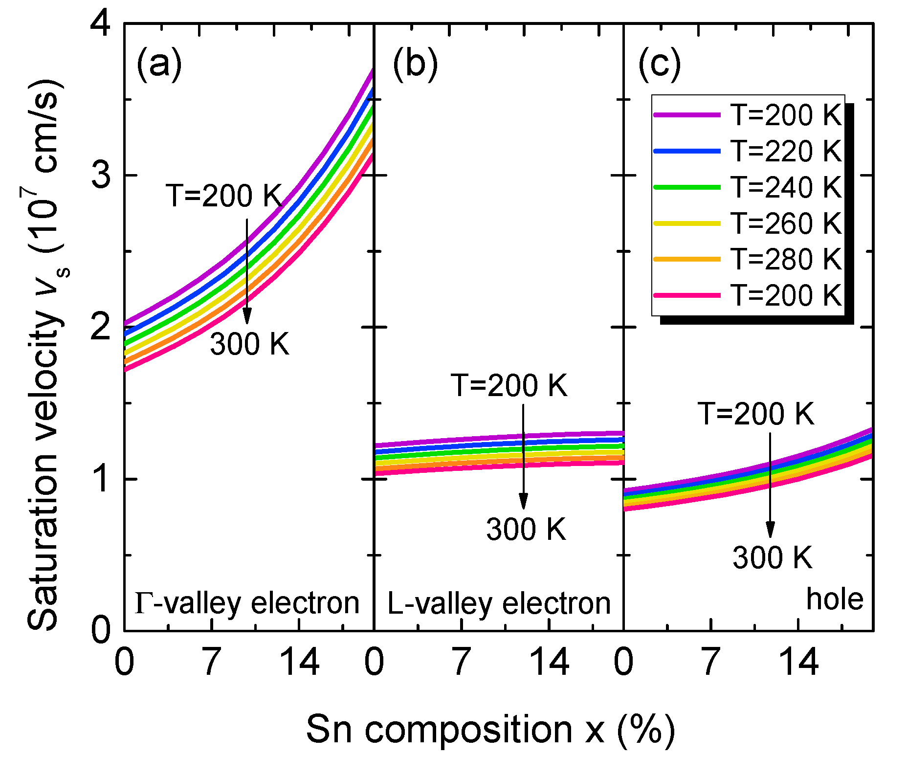
Figure 7 shows the calculated saturation velocities of electrons in the Γ-CB and L-CB and holes in the valence band as a function of Sn content at various temperatures. For a fixed temperature, the saturation velocities increase with increasing Sn content, because of the increased carrier mobilities. As the temperature increases, the electron and hole saturation velocities decrease because of the reduced mobilities. For electron saturation velocities, electrons in the Γ-CB have much higher saturation velocities then these in the L-CB, because of their much smaller effective mass (
m*=0.045 – 0.166
x + 0.043
x2 for Γ-CB electrons and for
m*=0.566 – 0.449
x + 1.401
x2 for L-CB electrons [
32]). On country, the hole saturation velocity is much smaller than the electron ones, because of the much larger effective masses. Thus, when electron-hole pairs are created by the absorption of incident photons in the GeSn active region, holes require longer time to transit through the active region than electrons. As a result, the transit-time-delay-limited bandwidth is dominated by the transition time of holes.
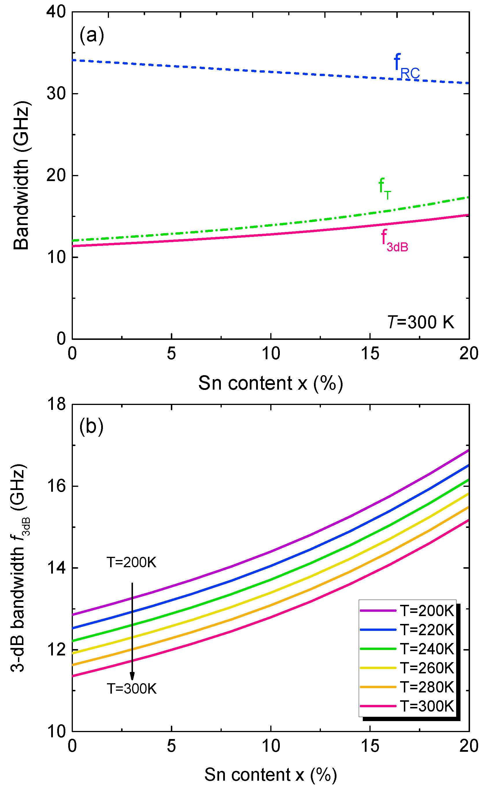
Figure 8a depicts the calculated transit-time-delay-limited, RC-delay-limited, and 3-dB bandwidth of the GeSn PD as a function of Sn content at
T=300K. The transit-time-delay-limited bandwidth decreases with increasing Sn content as a result of increased carrier saturation velocity. On the other hand, the RC-delay-limited bandwidth decreases with increasing Sn content owing to the increased permittivity of the GeSn active layer. However, transit-time-delay-limited bandwidth is significantly lower than the RC-delay-limited bandwidth owing to the thick GeSn active layer. As a result, the 3-dB bandwidth is dominated by transit-time-delay-limited bandwidth. As the Sn content increases, the 3-dB bandwidth increases slightly and can be greater than 10 GHz, indicating the capacity of high-speed operation.
Figure 8b shows the calculated 3-dB bandwidth of the GeSn PDs as a function of Sn content in the temperature range of
T=200-300 K. With an increase in temperature, the 3-dB bandwidth slightly decreases, but can remain >10 GHz.
Author Contributions
Conceptualization, S.-Q.Y.; methodology, G.E.C.; validation, G.E.C., S.-Q.Y. and G.S.; formal analysis, G.E.C. and G.S.; data curation, G.E.C., S.-Q.Y. and G.S.; writing—original draft preparation, G.E.C.; writing—review and editing, S.-Q.Y., G.S. and G.E.C.; project administration, G.E.C., S.-Q.Y. and G.S., funding acquisition, G.E.C., S.-Q.Y. and G.S. All authors have read and agreed to the published version of the manuscript.
