1. Introduction
Heat dissipation in conventional complementary metal–oxide–semiconductor (CMOS) technology is a major challenge for the design and operation of integrated circuits (ICs). As CMOS technology scales down, the power density and the operating temperature increase, which can degrade the performance, reliability, and lifetime of devices [
1,
2].
Conventional computational processes usually involve irreversible operations that erase some input bits of information during the process. In 1961, Landauer [
3] proved that irreversible computations cause information loss and involve an amount of heat dissipation of
kBTln2 per bit erased, where
kB is the Boltzmann constant and
T is the temperature. In 1996, Gershenfeld [
4] argued that the actual amount of energy dissipated due to information loss is much higher than Landauer’s lower bound . As nanoelectronic circuits and systems decrease in size and become more efficient, their energy dissipation levels approach Landauer’s limit. Therefore, to continue the trend of reducing power consumption and to reach Landauer’s lower bound, unconventional computation methods, that allow for reversible logic operations without information loss, are needed [
5].
Reversible logic operations, which have a one-to-one correspondence between the number of input and output signals, are a promising alternative to conventional irreversible computations that lose information and consequently dissipate heat into the environment. In 1973, Bennett [
6] showed that reversible computations can theoretically avoid information loss and achieve zero energy dissipation. Reversible computing is a paradigm of computation that allows computational processes to be reversed in time, recovering previous states of the system. This property is essential for avoiding the increase in physical entropy and the associated energy dissipation that occurs when information is erased irreversibly. However, substantial energy reductions in reversible computing can only be obtained by maintaining reversibility down to the physical level [
7]. This means that not only the logical operations but also the physical devices and circuits, that implement them, must be reversible, to avoid energy dissipation.
Quantum-dot cellular automata (QCA) are a promising nanotechnology for implementing digital circuits that are logically and physically reversible and overcome the drawbacks of conventional CMOS-based very large-scale integration (VLSI) technology, including high power consumption and heat dissipation. In 1993, Lent et al. [
8] proposed a physical implementation of digital computation using quantum dots. QCA employs field-coupled nanotechnology (FCN), which encode information as the electron orientation polarity within quantum-dot cells and can be propagated to neighboring cells using the electrostatic interaction [
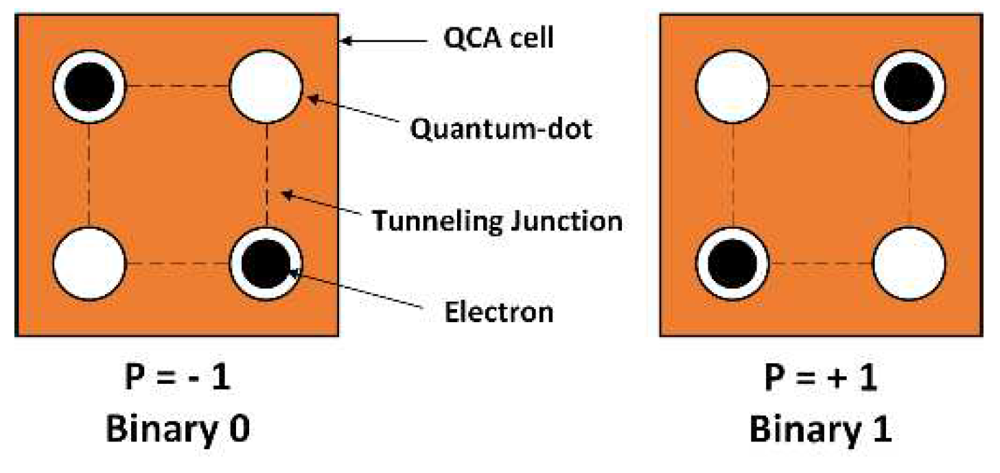
9]. The basic units in QCA circuits are QCA cells, which consist of four quantum dots placed at the corners of a square. Each cell has two free electrons that can tunnel between quantum dots, to represent two binary configurations. The two electrons tend to be located at opposing corners due to their electrostatic interactions. As illustrated in
Figure 1, the QCA cells can be in one of two states: cell polarizations of P = -1 or +1, which represent binary information of 0 and 1, respectively. Using arrays of quantum dots, QCA encodes binary information as the polarization of electrons. The specified circuit layout and electrostatic interactions among adjacent cells permit logic function implementation, and numerous studies have investigated QCA as a future computing technology [
10,
11,
12].
The arithmetic logic unit (ALU) is an essential component of the central processing unit (CPU) of every computer system, that performs digital logical and arithmetic operations with binary numbers. Combinational logic circuits are commonly utilized in the process of developing ALU circuits. The majority of the current QCA ALU designs in the literature are irreversible, yet reversible circuits are known to increase energy efficiency. Recently, numerous studies on reversible QCA ALU designs have been conducted [
13,
14,
15,
16,
17,
18]. However, these studies have addressed reversibility only at the logical level and have not treated information loss at the physical layout level. These studies used either well-known logically reversible gates, such as the 3 × 3 Fredkin gate or the 2 × 2 Feynman gate, or newly suggested logically reversible gates, to design reversible ALUs. The equal number of input and output pins on the netlist of these designs is insufficient to make them physically reversible and obtain ultralow-energy dissipation ALUs. This is because the internal majority gates that make up these ALUs are not reversible, i.e., the number of input and output pins for each internal majority gate is not the same. In 2020, Torres et al. [
19] designed and simulated a logically and physically reversible QCA half-adder circuit for the first time using
QCADesigner-E software, a QCA circuit implementation and simulation platform pioneered by Torres et al. [
20].
QCADesigner-E calculated the energy dissipation values of the QCA half-adder circuit and confirmed that the logically and physically reversible combinational QCA circuits could be operated with near-zero energy dissipation, i.e., values lower than
kBTln2 per operation. Later, researchers implemented this technique to develop more sophisticated combinational QCA logic circuits, as well as sequential QCA circuits, characterized by feedback loops [
21,
22]. In this study, we present the first implementation of the logically and physically reversible QCA design approach, to developing a multilayer reversible QCA ALU. This ALU design relies mainly on the majority gate as the core building block and uses the universal, standard, and efficient (USE) clocking scheme to synchronize data propagation. Our simulation results confirm that the logically and physically reversible design technique can yield an ultralow energy dissipation QCA ALU. The remainder of this paper is organized as follows: In
Section 2, QCA clocking schemes are reviewed. In
Section 3, the energy behavior of QCA cells is examined. In
Section 4, the logically and physically reversible design method is defined. In
Section 5, the multilayer logically and physically reversible QCA ALU design and simulation setup are described. Then, the simulation results are discussed in
Section 6, and the conclusions of the study are stated in
Section 7.
2. QCA Clocking Schemes
To ensure proper data transfer and operation in logic circuits, clocking control plays a vital role in coordinating data flow. For QCA, an external clock is needed to change the tunnelling barrier strength between the QCA cells and achieve clocking control. Various clocking and timing methods have been proposed to regulate the data propagation through QCA circuits.
In 1997, Lent and Tougaw [
9] proposed a method of adiabatic switching that enables time control, solves metastability issues, and facilitates pipelined construction for QCA circuits [
9]. This clocking method enables the QCA array to be divided into groups of cells called clock zones, providing the benefits of multiphase clocking and pipelining. With the clock zone system, a group of QCA cells can execute a computation, have its states frozen, and feed its results into the next clock zone, as inputs. Furthermore, partitioning the QCA wire into zones is similar to splitting it into multiple tiny wires, as allowing the QCA wire length to grow can increase the likelihood that cells will not switch correctly, due to thermodynamic constraints [
23].
Figure 2 is a schematic representation of the four phases of an adiabatic pipelining cycle. Each box represents the condition of a subsystem of multiple cells. Each cell in the subsystem has the same gate regulating the inter-dot barriers. The schematic cell on the left within each frame represents the state of the cells at the commencement of this clock phase, whereas the cell on the right represents the state of the cells at the end of this clock phase. We emphasise that although only two cells are depicted in each subarray, they are representative of a greater number of cells. Throughout the first phase, known as the switch phase, the cells are initially unpolarized and have low barriers, but during this phase, the barriers are elevated and the cells become polarised according to the state of their driver. This is the phase of the clock during which computations are performed. By the end of this phase of the cycle, the barriers are sufficiently high to prevent tunnelling, and the cell states are essentially fixed. During the subsequent clock phase, the hold phase, the barriers are held at this high value so that the subarray's outputs can be used as inputs for the subsequent stage. Next, during the release phase, the barriers are lowered and the cells are permitted to enter a depolarized state. During the fourth phase of the clock, the relaxed phase, the cell barriers remain reduced, maintaining the cells' neutral, unpolarized state. After this fourth phase, the subsystem will repolarize and revert to the initial clock phase, starting a new cycle.
In the adiabatic switching method the input states are switched gradually while the interdot barriers of the cells are modulated simultaneously across the entire array, thus keeping the system always in its instantaneous ground state. Furthermore, QCA clocking can be used to synchronize the information, avoiding having a signal reach a logic gate and propagate before other inputs reach the gate. These characteristics are extremely important for QCA circuits, guaranteeing their correct operation. However, there are many limitations to implementing this one-dimensional adiabatic switching paradigm, such as a substantial difference in wire lengths, clock zones with nonuniform capacity, a large difference in the number of cells between zones preventing the implementation of feedback paths, and unused area [
24].
In 2007, a two-dimensional QCA clocking method was proposed by Vankamamidi et al. [
25]. The two-dimensional QCA clocking method can achieve higher performance and lower power consumption, than a one-dimensional QCA clocking method, by exploiting the spatial and temporal parallelism of QCA circuits. This clocking scheme takes zone size into account and comprises a grid of square zones that are equal in size, thus preventing thermodynamic effects on QCA circuits. The overhead of feedback channels, however, remains a major challenge [
24]. Additionally, long lines between clocking zones in advanced QCA circuits have a negative impact, leading to higher delay and more sensitivity to thermal fluctuations [
24].
In 2016, Campos et al. [
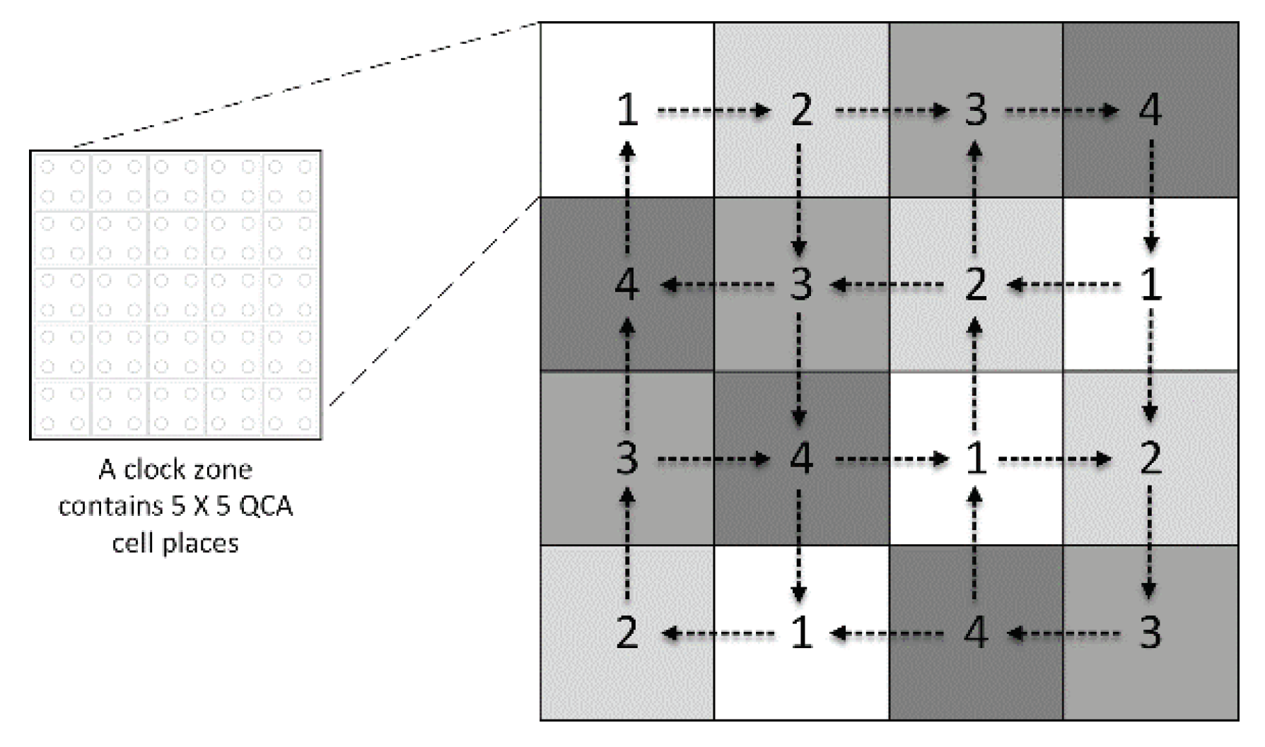
24] developed the universal, standard, and efficient (USE) clocking scheme. The USE clocking approach can meet the QCA cell requirement, implement feedback paths with small or large loops, standardize cell libraries and allow for routing simplification due to its flexibility.
Figure 3 shows the USE clocking system, which consists of four time zones numbered from 1 to 4. These four time zones constitute a complete clock cycle. Data flows between QCA cells in neighboring clock zones, shown here as squares. Each square represents a clock zone and comprises a cluster of 5 × 5 QCA cells.
To balance the speed of data transmission and ensure that the data arrival time is accurate for each logic gate in the circuit, clock synchronization is an essential metric [
26]. It is crucial to distinguish between local and global synchronization when evaluating QCA circuits.
Local synchronization necessitates that data transmission be restricted only between cells in clock zones with consecutive numbers.
Global synchronization ensures that new data are transmitted to the primary inputs of the circuit during each clock cycle; thus, the inputs of all gates are synchronized for at least one clock cycle prior to the arrival of new data. Most researchers emphasize that local synchronization is an essential requirement to include when developing QCA circuits [
26,
27,
28,
29]. However, the literature on global synchronization is contradictory. Despite many related assertions highlighting the significance of global synchronization [
27,
28], some studies argue that global synchronization is not a compulsory constraint for QCA circuits [
29].
Real clocking is a crucial feature of developing QCA circuits, as it may significantly reduce production costs and simplify the physical implementation of QCA circuits. The real clocking concept was incorporated into the QCA clocking techniques in either pipeline style [
25] or dynamic style [
24,
29]. The real clocking approach, with efficient clustering and placement, was recently developed for complicated circuits that are based on five-input majority gates [
30]. The real clocking technique is generally efficient for QCA circuits that use majority gates with more than three inputs [
30].
In this study, the proposed multilayer logically and physically reversible QCA ALU design employs the USE clocking scheme [
24] to precisely regulate the dataflow between the cells and prevent the system from being stuck in a metastable state. Because of its flexibility, the tile-based USE clocking methodology enables the creation of feedback paths with small or large loops, simplifies the routing process, and creates clock zones with uniform, regular, and bounded forms. Furthermore, current integrated circuit design and fabrication technologies can be utilized to realize USE clocking circuitry. In complex QCA digital circuit designs, clock synchronization, both local and global, is essential to ensure the balance of the data propagation speed and guarantee that the data arrival time is correct for the next stage in the circuit [
31]. The absence of clock synchronization constraints can lead to the generation of inaccurate bits in the next stage, resulting in incorrect data transmission. In our proposed ALU, data are transferred between cells in consecutively numbered clock zones. Furthermore, the input data for each logic gate arrives within four clock phases, i.e., during the same clock cycle. This guarantees that our ALU design is both locally and globally synchronized and should generate correct computation results.
3. Energy Behavior of QCA Cells
QCA cells start the clock cycle in a depolarized state. They need energy from the clock to reach a polarized state. Most of this energy goes back to the clock and other cells when the cell depolarizes again, at the end of the clock cycle. However, some energy is dissipated to the environment. To study the energy loss of QCA cells, the microscopic quantum mechanical model of QCA cell behavior based on the coherence vector formalism is employed [
20,
31,
32,
33].
In the microscopic quantum mechanical model, incorporated in the
QCADesigner-E software package, the state of a QCA cell is captured by two three-dimensional vectors:
and
. The coherence vector
represents the expectation value of the Pauli matrices within the density matrix formalism and reflects the current state of the cell, where
corresponds to polarisation [
20]. The energy vector
, with
being the reduced Planck constant, is derived from the Cell Hamiltonian:
The cell Hamiltonian involves matrix elements describing the tunneling coupling (γ) between dots and the Coulomb force exerted by neighboring cells ().
The kink energy between two cells,
i and
j, measures the energy cost of having opposite polarizations. The polarization of a cell is determined by the position of the two excess electrons in the four quantum dots that form the cell. The polarization of a cell can be influenced by the polarization of its neighboring cells through Coulombic interactions given by:
indicates Coulombic interactions with neighbourhood cells of the cell and this interaction depends on the polarization of the other cells as well as the kink energy between cells i and j.
To calculate the expectation value of the energy
of a QCA cell, the formula
must be used, where
is the trace operator,
is the Hamiltonian of the cell, and
is the density matrix of the cell. The Hamiltonian describes the tunneling coupling within a cell, and the Coulomb interaction between electrons and the external electric field due to the clock. The density matrix
represents the statistical state of the cell, such as the probability of finding an electron in a certain quantum dot. By taking the expectation value of
with respect to
, we can obtain the average energy of the cell at any given time. Exploiting the linearity of the
operator and using
, we can model the energy dissipation of a QCA cell as a function of time:
This expression allows us to represent the instantaneous power
of a QCA cell as:
The function
denotes the current energy of the cell at time
and is essentially given as the scalar product of the two energy vectors at that point in time. Consequently, the total energy dissipation of a QCA cell
during a complete clock cycle with period
is given as the integral of
over one cycle:
The integrand of Equation (3) is the scalar product of the derivative of the energy vector
and the coherence vector
of the cell. This expression can describe the energy transmission within the clock
and neighbouring cells
that occurs during a clock cycle [
20,
31,
32] and can be calculated as:
Moreover, it can capture the energy transfer to the environment
within a clock cycle [
20,
31,
32].
represents the dissipated energy of a QCA cell during a clock cycle and can be calculated as:
where
refers to a technology-dependent relaxation time parameter and
denotes the thermal ratio and given by:
As indicated in [
32,
34], the system is always approaching the thermal steady state; thus, to ensure the validity of the calculations, there must be numerical energy conservation, i.e., the total energy must be zero:
4. Logically and Physically Reversible Design Methodology
Designing logically and physically reversible QCA circuits is quite challenging, as it requires a sophisticated technique that guarantees that reversibility is sustained from the logical to the physical level of the design. The term "logically reversible" is used to describe a netlist in which the number of input and output pins is the same. However, this does not guarantee that the utilized QCA internal logic gates, composed of majority gates, are also reversible, with the same number of input and output pins. "Physically reversible" means that each and every majority gate component, in the circuit, must have the same number of input and output pins. Consequently, there is both no information loss and no associated energy dissipation into the environment. Indeed, reversible computing is an effective low-power technique, only if reversibility is sustained down to the physical layout level [
7].
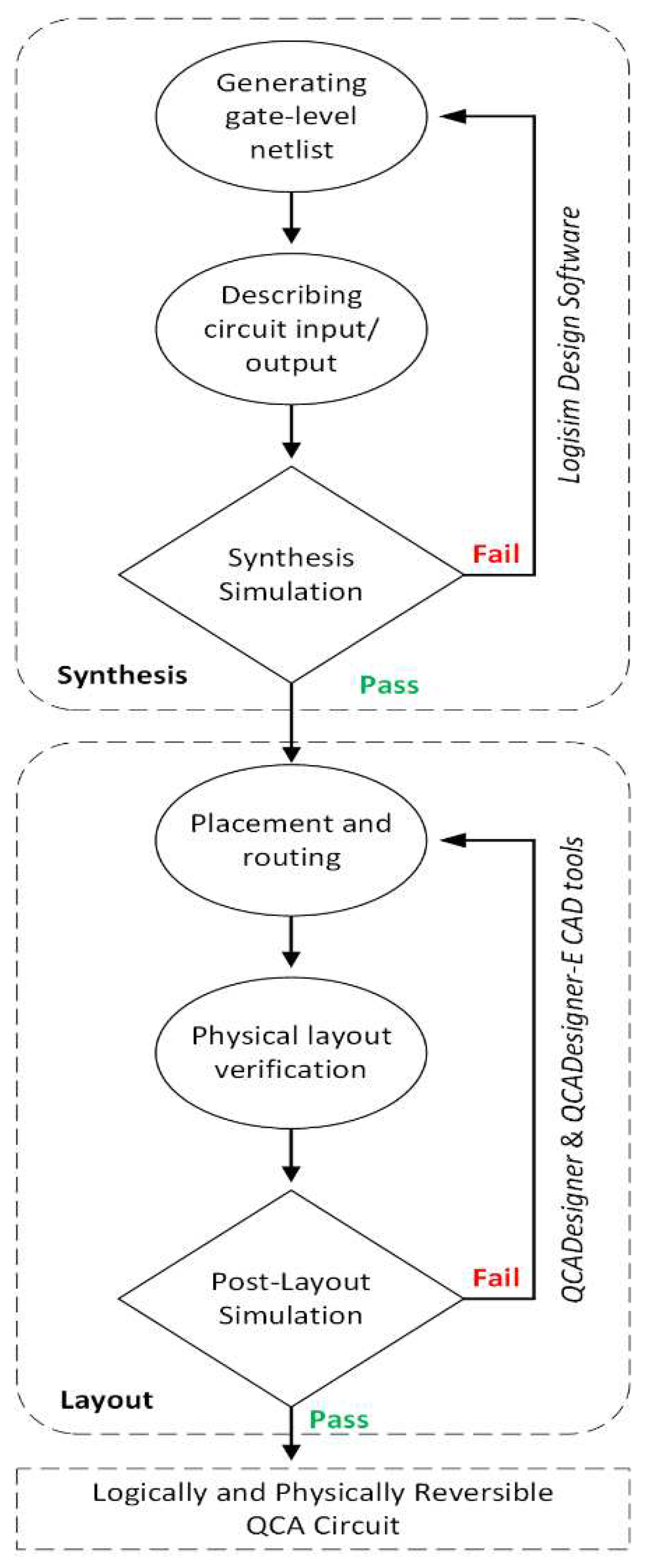
The implementation method in this study for designing the proposed logically and physically reversible QCA ALU circuit comprises two main stages: developing the circuit at the logical level (synthesis) and then developing the circuit at the physical level (layout) based on QCA interconnected devices, as shown in
Figure 4.
At the logical level, the circuit design is composed of structural and behavioral descriptions. The structural description comes first, describing and generating a netlist of the circuit. The behavioral description follows, describing the design as a set of input–output relations. Finally, simulations are performed to validate the circuit synthesis. Logisim software was utilized at this stage to develop circuit synthesis and conduct behavioral simulations.
The physical level represents the circuit transition from synthesis to a QCA layout, which is the physical representation of the circuit. This process started with the pins’ locations, gate placement, and routing. Next, layout verification is performed to validate that the layout reflects the circuit synthesis design. Finally, post layout simulation is performed to validate both the circuit performance and reliability, as well as evaluate the energy dissipation values. For this purpose, the widely used QCA technology-based computer-aided design (TCAD) tool
QCADesigner was employed in this study.
QCADesigner implements the coherence vector simulation engine (CVSE), which incorporates the quantum-level microscopic physical modelling of the QCA cell performance (see
Section 3) [
35].
QCADesigner is used to evaluate the QCA circuit’s performance, area cost, latency, and reliability.
In QCA circuits, the main source of energy dissipation is the majority gate [
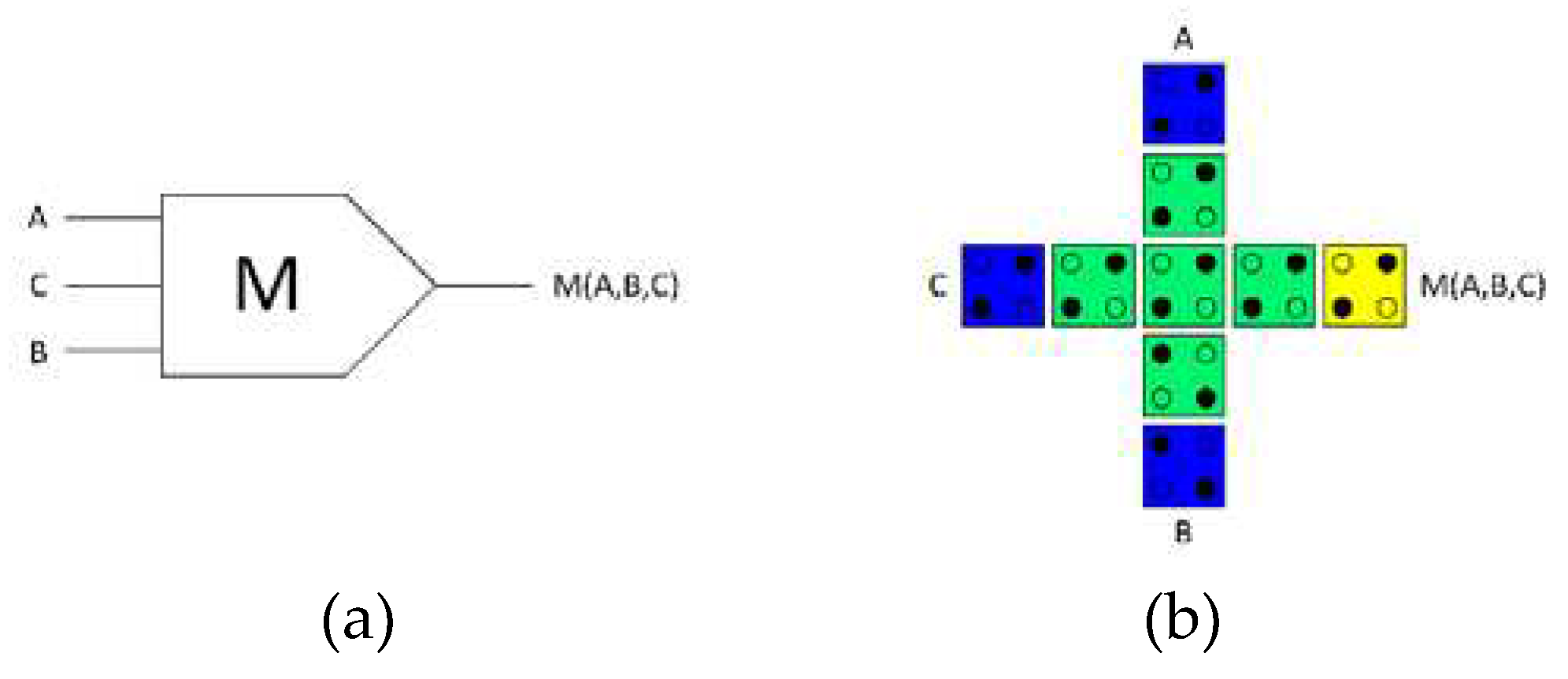
36]. The conventional QCA majority gate is irreversible; it has three inputs and one output, as shown in
Figure 5. Therefore, it has energy dissipation into the environment associated with information loss.
Figure 5a depicts the logical design (schematic), whereas
Figure 5b depicts the physical design (layout) of a standard irreversible majority gate.
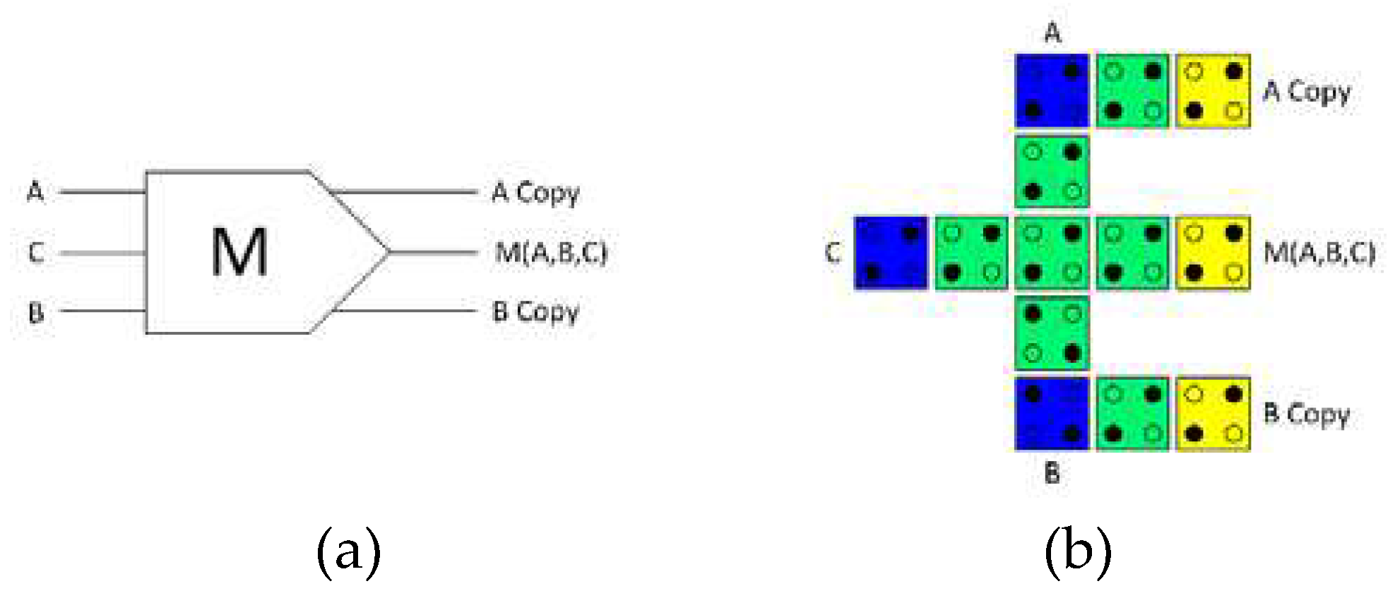
To develop a highly energy efficient QCA ALU in this study, the logically and physically reversible design approach was taken for designing a fully reversible majority gate, which is the key component in our design. The fully reversible majority gate generates copies of the input data, resulting in the same binary inputs and outputs. The proposed fully reversible QCA majority gate illustrated in
Figure 6 generates copies of the input data and has three inputs and three outputs. Therefore, there is no information loss and no associated energy dissipation to the environment. Fig. 6a illustrates the logical design (schematic), while
Figure 6b illustrates the physical design (layout) of the fully reversible QCA majority gate design.
To simulate the energy dissipation levels for QCA designs, an appropriate tool is needed. Presently, two TCAD tools are available for simulating the energy dissipation of QCA circuits:
QCADesigner-E, which was introduced by Torres et al. [
20], and
QCAPro, which was developed by Srivastava et al. [
31]. The
QCAPro simulation tool requires an ideal clock slope and can yield a higher limit for energy dissipation. In contrast,
QCADesigner-E can accurately calculate the energy dissipation values. The
QCADesigner-E simulation tool is based on the widely used
QCADesigner software package. The
QCADesigner-E tool was selected to simulate the energy dissipation of the proposed logically and physically reversible QCA ALU design, owing to its incorporation of a proper energy dissipation treatment based on the application of quantum mechanics QCA cells, a rigorous microscopic treatment. Moreover,
QCADesigner-E extends the CVSE model of
QCADesigner to include power dissipation.
The CVSE is a fixed timestep transient analysis, where new values for the components of the coherence vector and the tunnelling energy are calculated in each iteration step. The evolution of the coherence vector λ is determined by solving the differential equations that represent the evolution of the quantum mechanical density matrix using an iterative fixed timestep approach [
20]. The cell polarization is identical to the coherence vector component, while the kink energies are precomputed values determined by the design architecture. The kink energy of a pair of cells is a static measure determined by the electrostatic interactions between all the charges of both cells. The time interval of each iteration step (
Tstep) and other technology and simulation parameters need to be adjusted to adapt to a specific QCA circuit design.
In the present research, the time interval used for each iteration (
Tstep) was 0.1
τ = 0.1
fs, where
τ is the relaxation time. A sufficiently small timestep is crucial for decreasing the simulation error and obtaining accurate results. This time step results in simulation errors with an acceptable numerical energy conservation violation, given by ϵ
env ≤ 5%. All the technology and simulation parameters utilized in this study are listed in
Table 1.
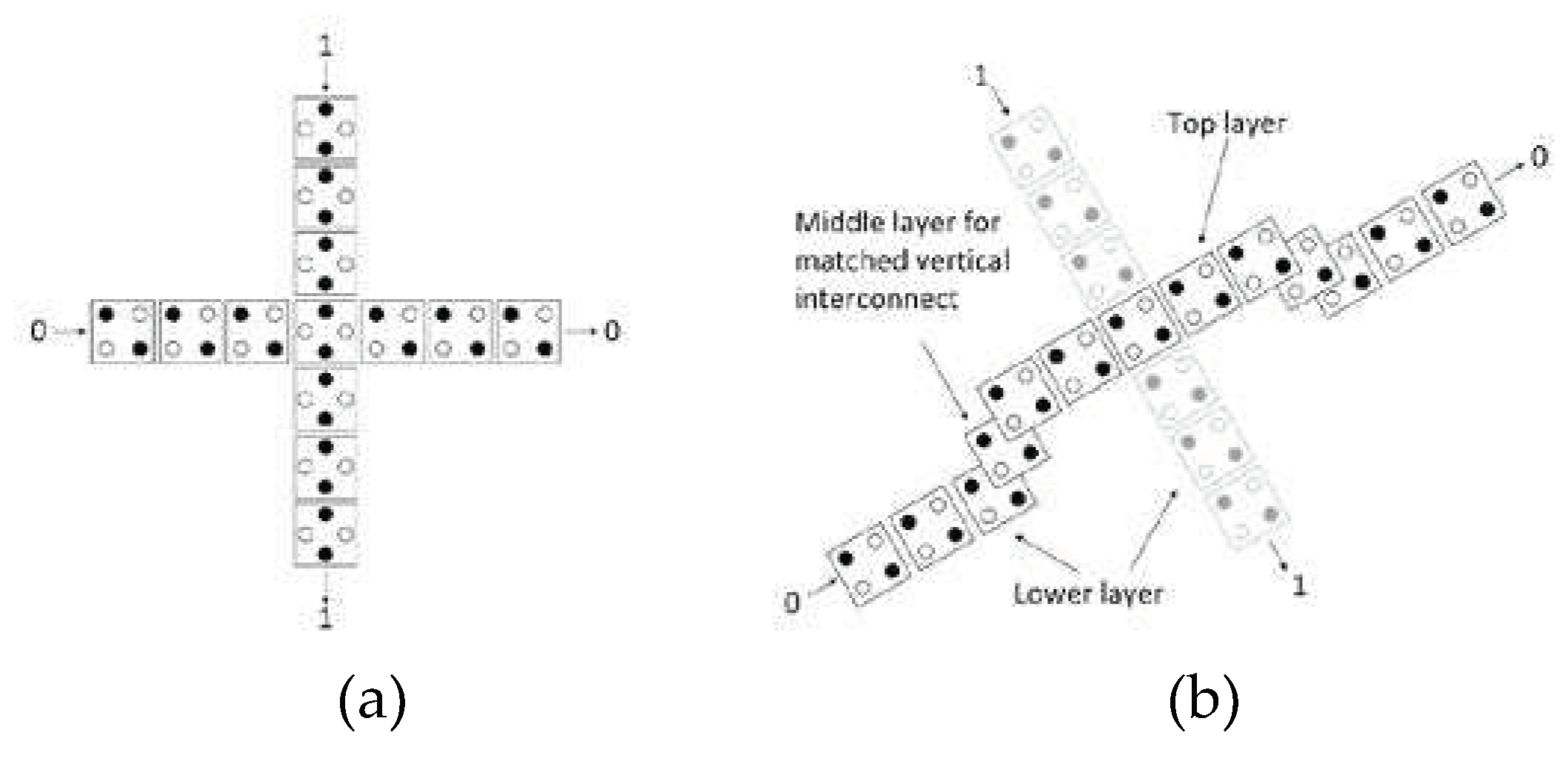
Dealing with wire junctions is one of the main challenges in digital design. In QCA technology, wires can be crossed using the coplanar method, as illustrated in
Figure 7a, requiring rotating QCA cells at the crossing site. Another solution for crossing wires is the multilayer method, as depicted in
Figure 7b, in which three distinct layers are utilized to prevent crosstalk interference between the crossing wires [
37]. Although the coplanar approach is a classic advantage of using the QCA paradigm and is incorporated into most designs, the use of the multilayer method results in more robust circuits [
38]. In this study, the reversible QCA ALU design employed the multilayer approach for wire crossing, as proposed by Bajec and Pecar [
39].
5. Proposed Logically and Physically Reversible QCA ALU Design
The ALU is a crucial component of the CPU. It can perform various arithmetic and logical operations on the data that enters the CPU. The ALU receives input data from registers, memory, or other sources and outputs the result to another register, memory, or device. The fully logically and physically reversible QCA ALU presented in this study is designed to be ultralow-energy efficient. It was developed using a variety of combinational logic circuits that are designed based on the fully reversible QCA majority gate proposed in
Figure 6.
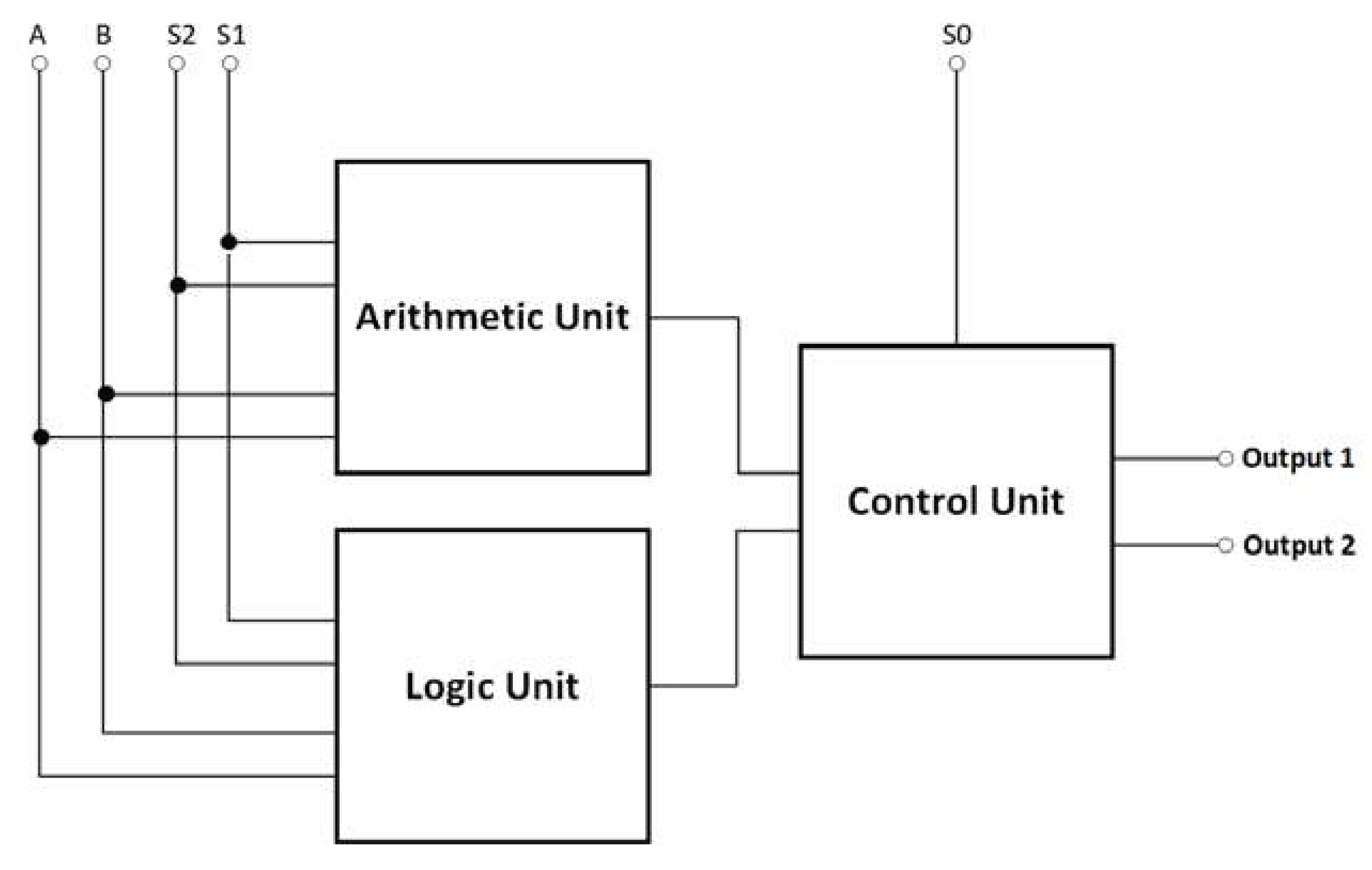
The development process began with the creation of a high-level block diagram, as depicted in
Figure 8. The reversible ALU architecture consists of three major components: the logic unit (LU), the arithmetic unit (AU), and the control unit (CU). The LU performs logical operations on data, including AND, OR, NAND, NOR, XOR, XNOR, NOT, and transfer. The AU performs arithmetic operations such as addition, subtraction, multiplication, and division on binary numbers. The CU specifies the type of operation to be conducted, either arithmetic or logic, according to its input S
0.
The reversible QCA ALU circuit receives two input operands, A and B, and then produces two output values, Output1 and Output2. By reversing Output1 to Output2, the reversible QCA ALU can perform two arithmetic or two logical operations simultaneously, giving a total of 16 operations, including 8 logical and 8 arithmetic operations, as shown in
Table 2. Three select input pins, labelled S0, S1, and S2, are utilized in the process of determining the operation function of the reversible QCA ALU and which operands to use.
Each block's synthesis is carried out first and simulated with the objective of validating the circuits' behavior.
Figure 6a depicts the schematic of a logically and physically reversible majority gate, which is used as the basic component for circuit synthesis development. Logical synthesis designs for AU, LU, and CU were developed. The design of logical synthesis includes defining and generating the netlist and input–output relationships of the circuits. At this point, simulation was performed using the
Logisim software to validate the performance of each circuit synthesis. Note that in the reversible logic circuit synthesis diagrams, the "cp" labels of the outputs refer to copies of the input information, and "g" indicates the so-called garbage outputs.
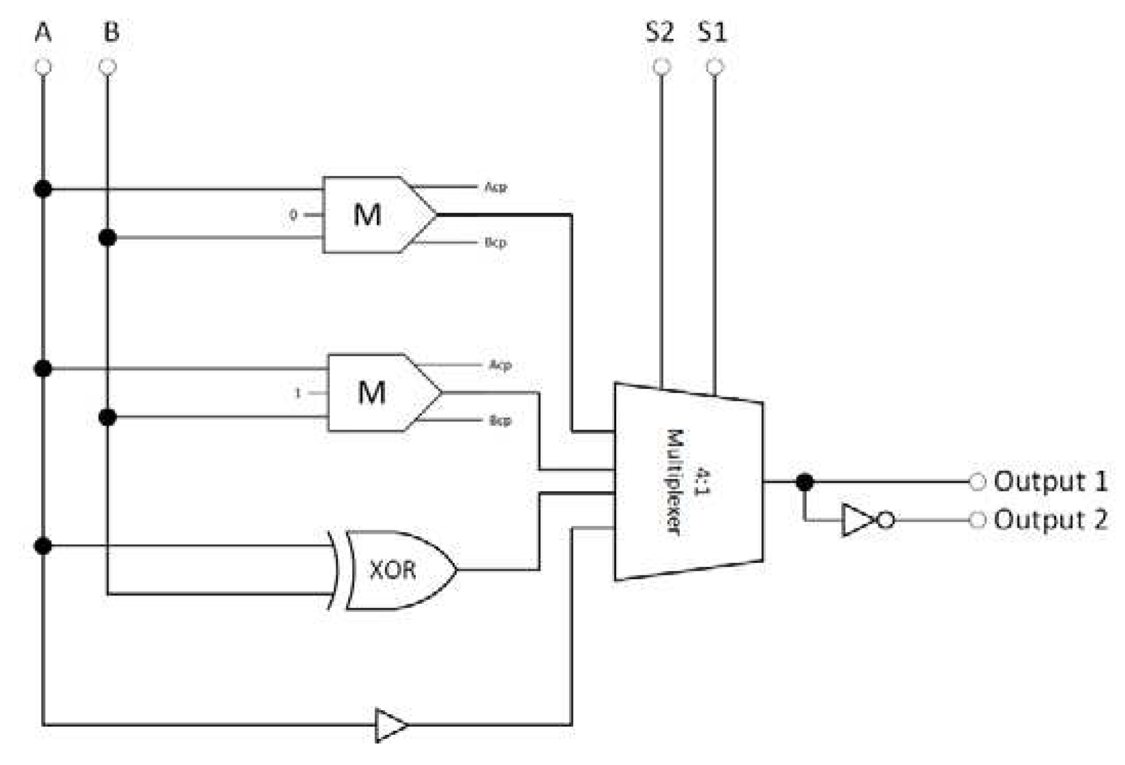
Figure 9 shows the proposed reversible LU. It consists of two reversible majority gates, an XOR gate, an inverter, a buffer, and a 4-to-1 multiplexer to perform eight logic operations.
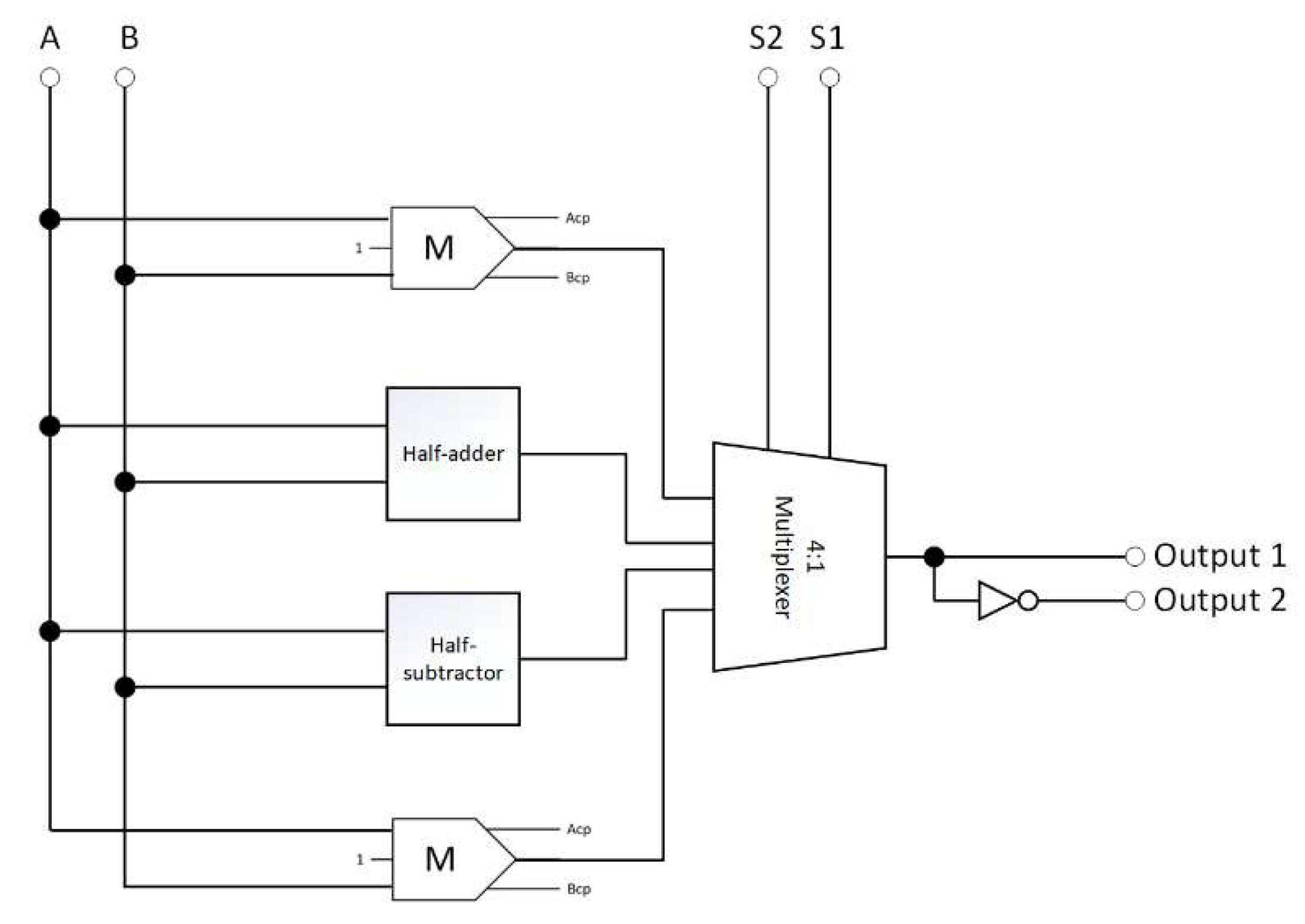
Figure 10 illustrates the proposed reversible AU, which consists of a half-adder, a half-subtractor, two majority gates, an inverter, and a 4-to-1 multiplexer and can execute eight arithmetic operations.
Then, the internal components required for constructing the reversible LU and AU were developed. The circuits that compose the proposed reversible LU and AU are the reversible XOR, half-adder, half-subtractor, and 4:1 multiplexer. Each circuit was meticulously designed, and its reliability was proven through simulation.
The synthesis of the proposed reversible XOR circuit is shown in
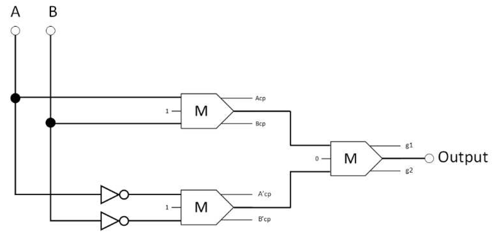
Figure 11. This XOR consists of three majority gates and two inverters. The Boolean expression for the proposed XOR logic circuit output is the standard one and is given by Equation 12.
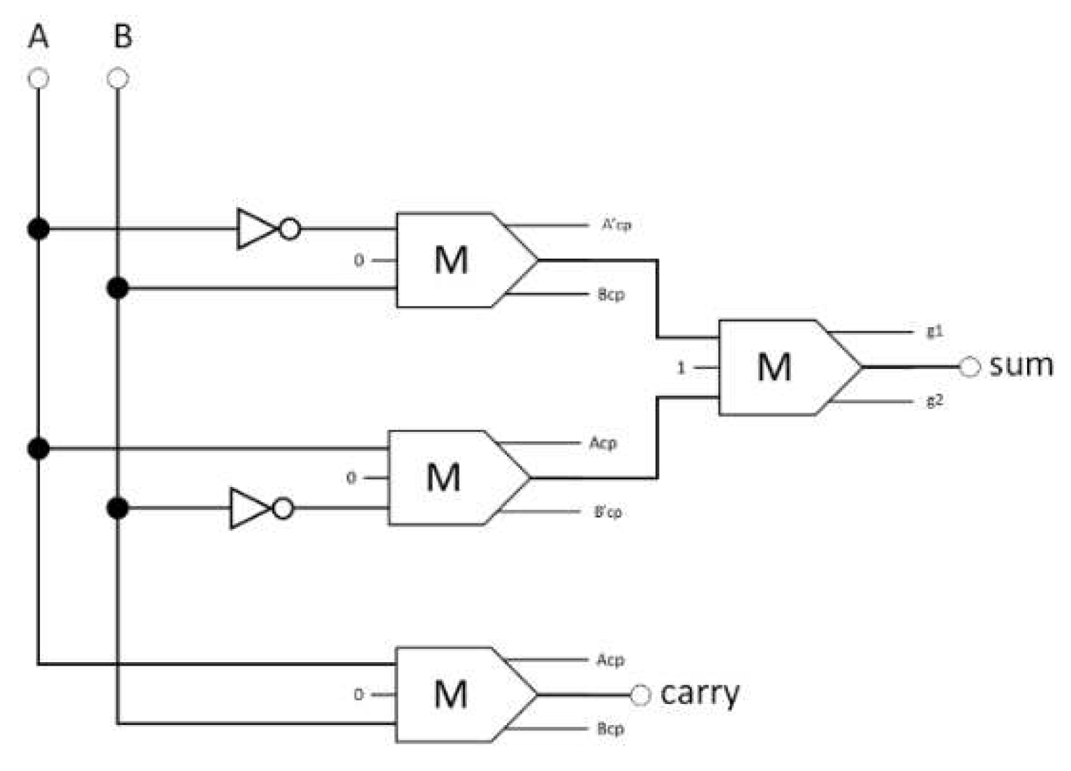
Four majority gates and two inverters make up the proposed half-adder circuit, as shown in
Figure 12. Equation 13 describes the Boolean expressions for this circuit:
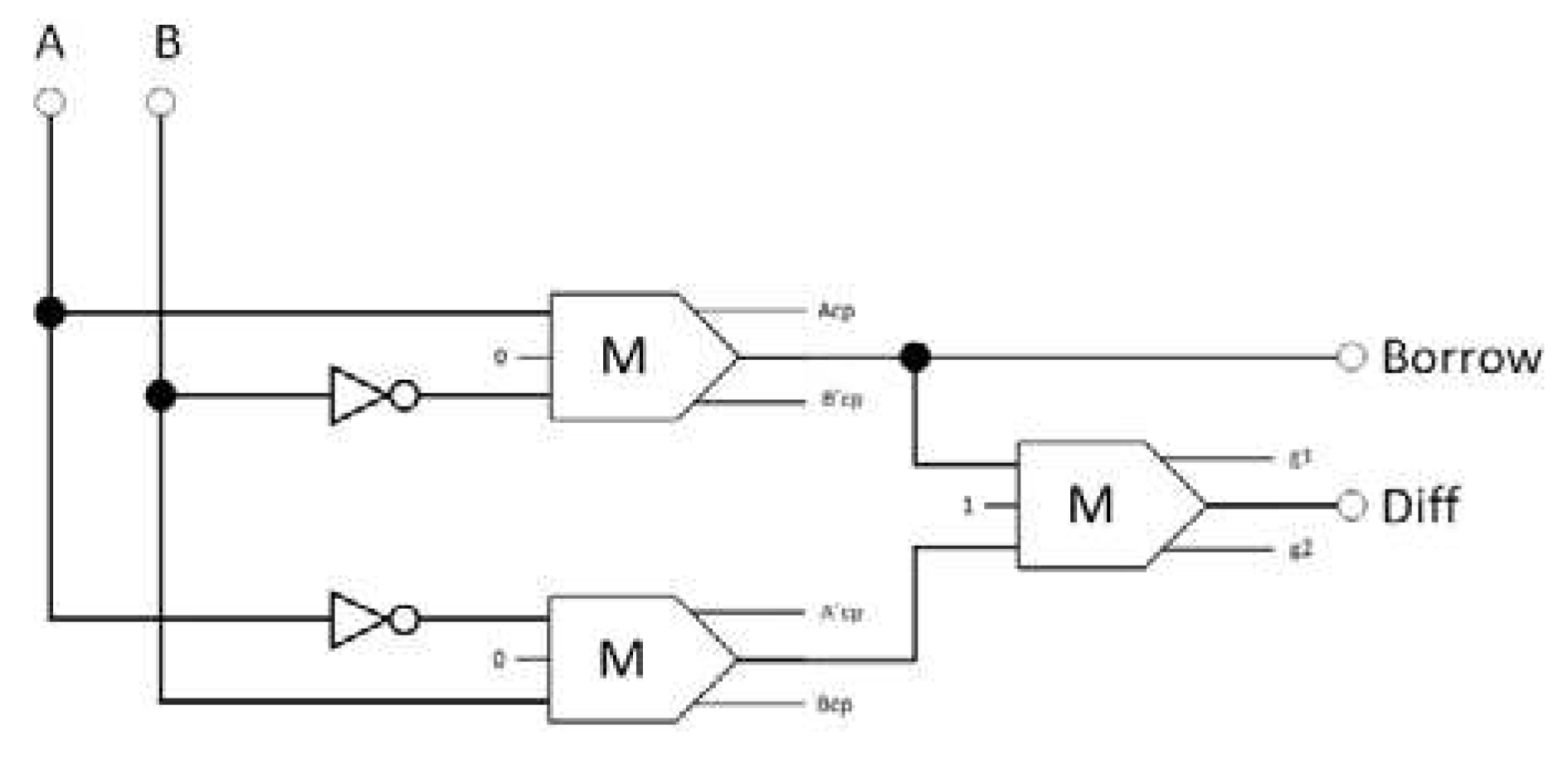
Figure 13 is an illustration of the suggested circuit for the reversible half-subtractor, which consists of three majority gates and two inverters. Equation 14 provides the definition for the Boolean equations that describe the design outputs.
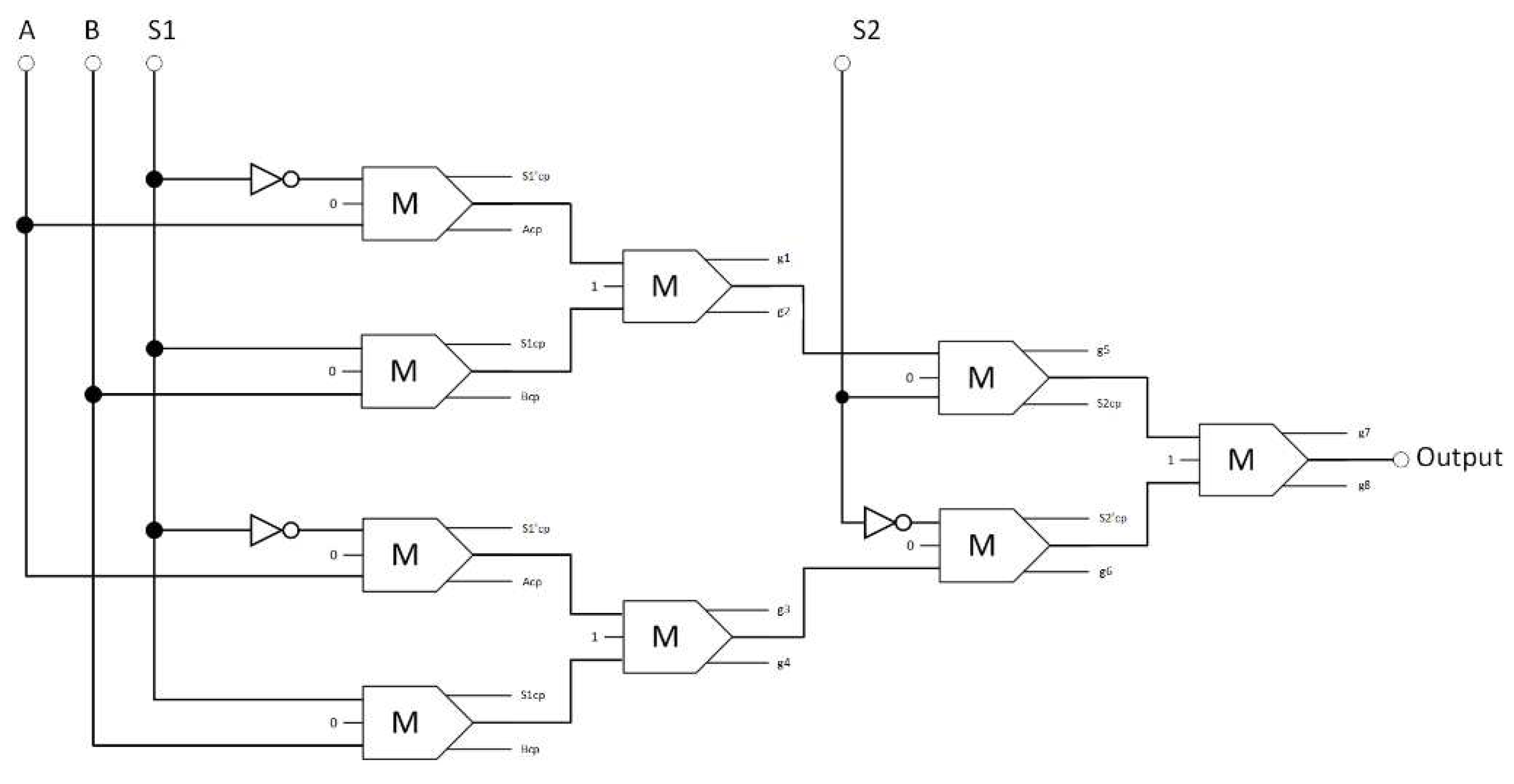
The proposed circuit for the reversible 4-to-1 multiplexer is depicted in
Figure 14, which consists of nine majority gates and three inverters. Equation 15 specifies the Boolean equation that defines the design's output.
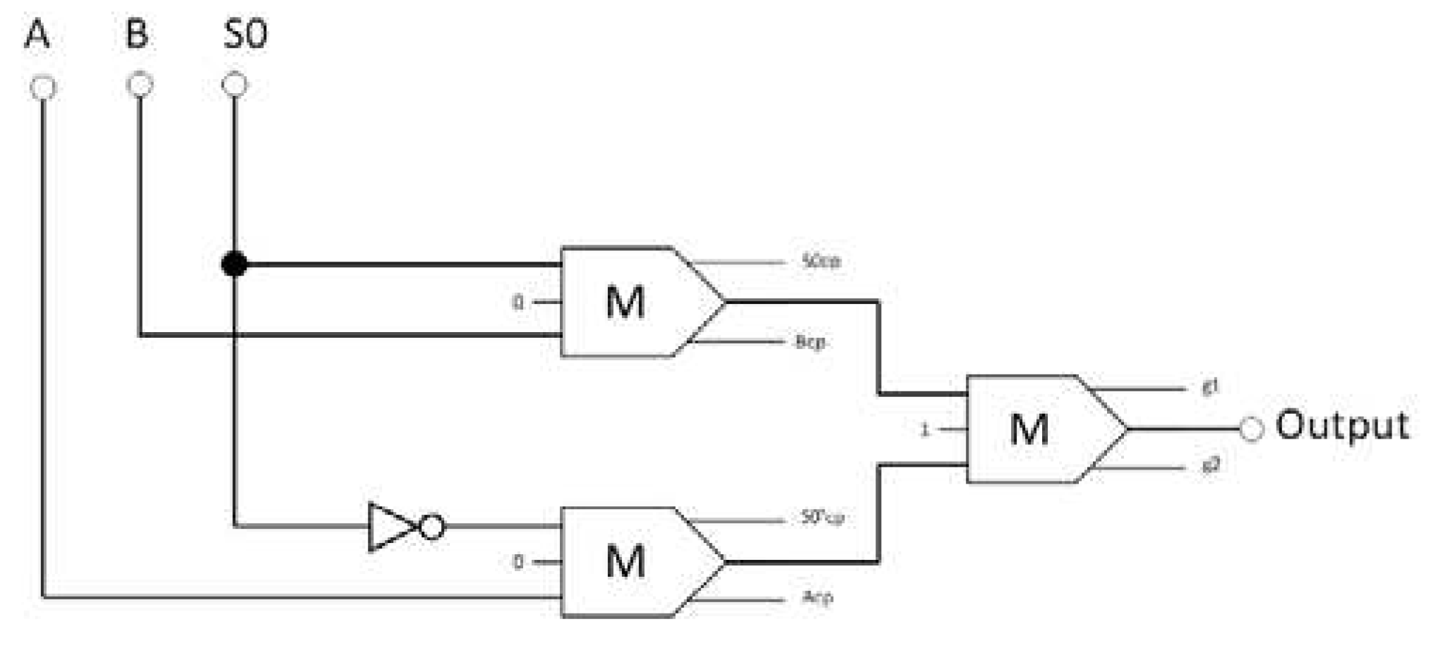
Next, the logical design of the CU was developed. As shown in
Figure 15, a reversible 2-to-1 multiplexer functions as a CU for turning on either the AU or the LU to execute an arithmetic or logic operation, respectively. This reversible 2-to-1 multiplexer comprises three majority gates and an inverter. Equation 16 is the Boolean expression for the output of the proposed 2-to-1 multiplexer circuit.
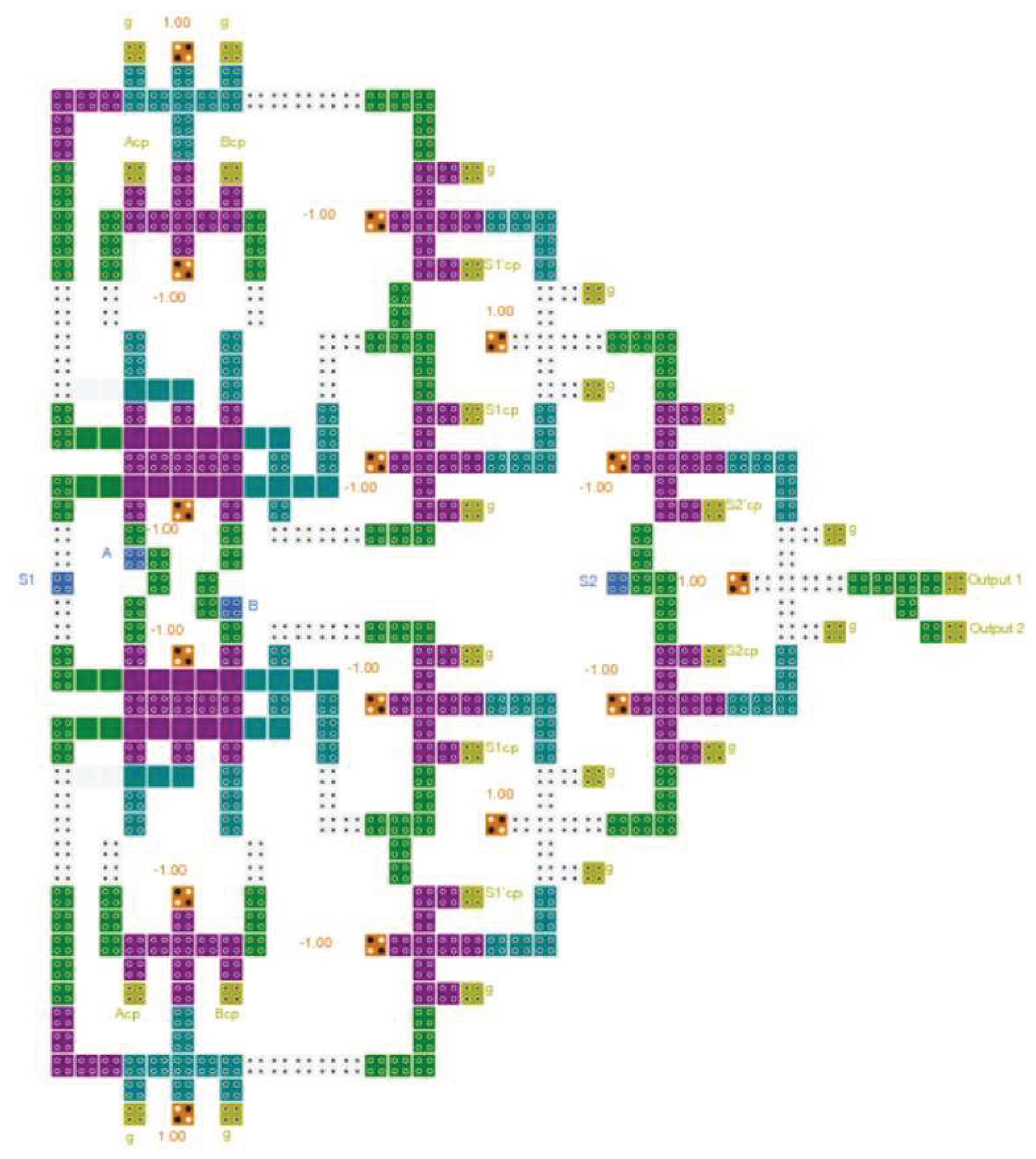
The logical synthesis of the circuits was then transformed into a physical layout that could be fabricated on a semiconductor chip. The layout development process involves numerous steps, including partitioning, placement, and routing. By interconnecting an array of QCA cells, the layout of a QCA circuit was designed. The layout of the logically and physically reversible QCA majority gate, depicted in
Figure 6b, was the basic building block for generating the overall QCA circuit layout.
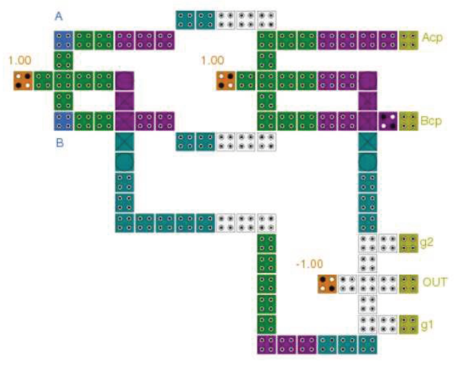
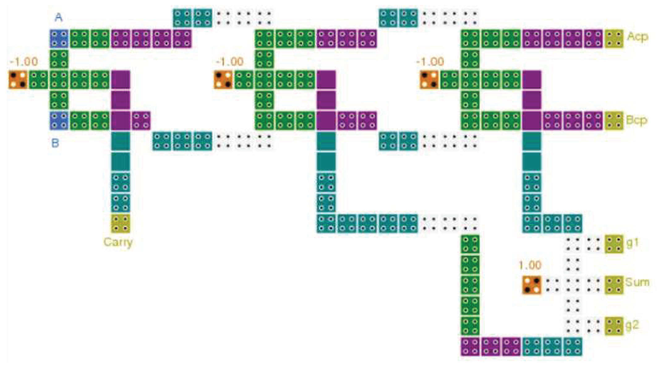
Initially, we created the layout configurations for the XOR, half-adder, half-subtractor, 2-to-1 multiplexer, and 4-to-1 multiplexer circuits based on the layout of the proposed fully reversible majority gate, as illustrated in
Figure 16,
Figure 17,
Figure 18,
Figure 19 and
Figure 20 respectively. Subsequently, the LU, AU, and CU that make up the multilayer reversible QCA ALU were built using these ingredient reversible QCA circuits. The LU, AU, and CU digital circuit blocks were then connected per
Figure 8 to yield the proposed reversible QCA-ALU layout. As in the reversible logic circuit synthesis diagrams, the "cp" designations of the outputs in the reversible QCA circuit layout architectures refer to copies of the input information, and "g" indicates the so-called garbage outputs.
As illustrated in
Figure 16, the proposed logically and physically reversible QCA XOR delay time is eight clock zones (two clock cycles), has an area of 0.15 µm
2, and employs 101 QCA cells.
Figure 17 shows that the proposed reversible QCA half-adder has a delay of 12 clock zones (three clock cycles), occupies 0.27 µm
2 of area, and requires 156 QCA cells for implementation.
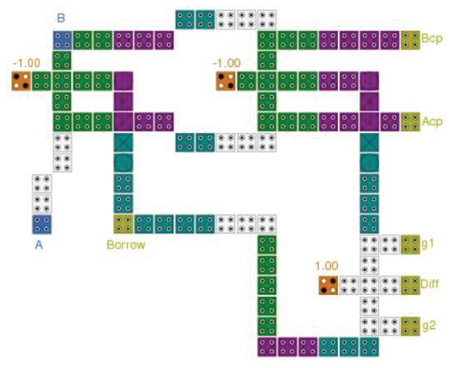
The reversible QCA half-subtractor latency is eight clock zones (two clock cycles), costs 0.15 µm
2 of area, and its implementation requires 116 QCA cells, as illustrated in
Figure 18.
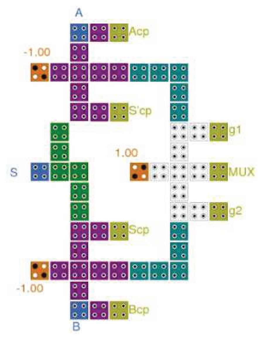
As demonstrated in
Figure 19, the reversible QCA 2-to-1 multiplexer has a delay of four clock zones (one clock cycle) and costs 0.09 µm
2 of area, and its implementation requires 56 QCA cells.
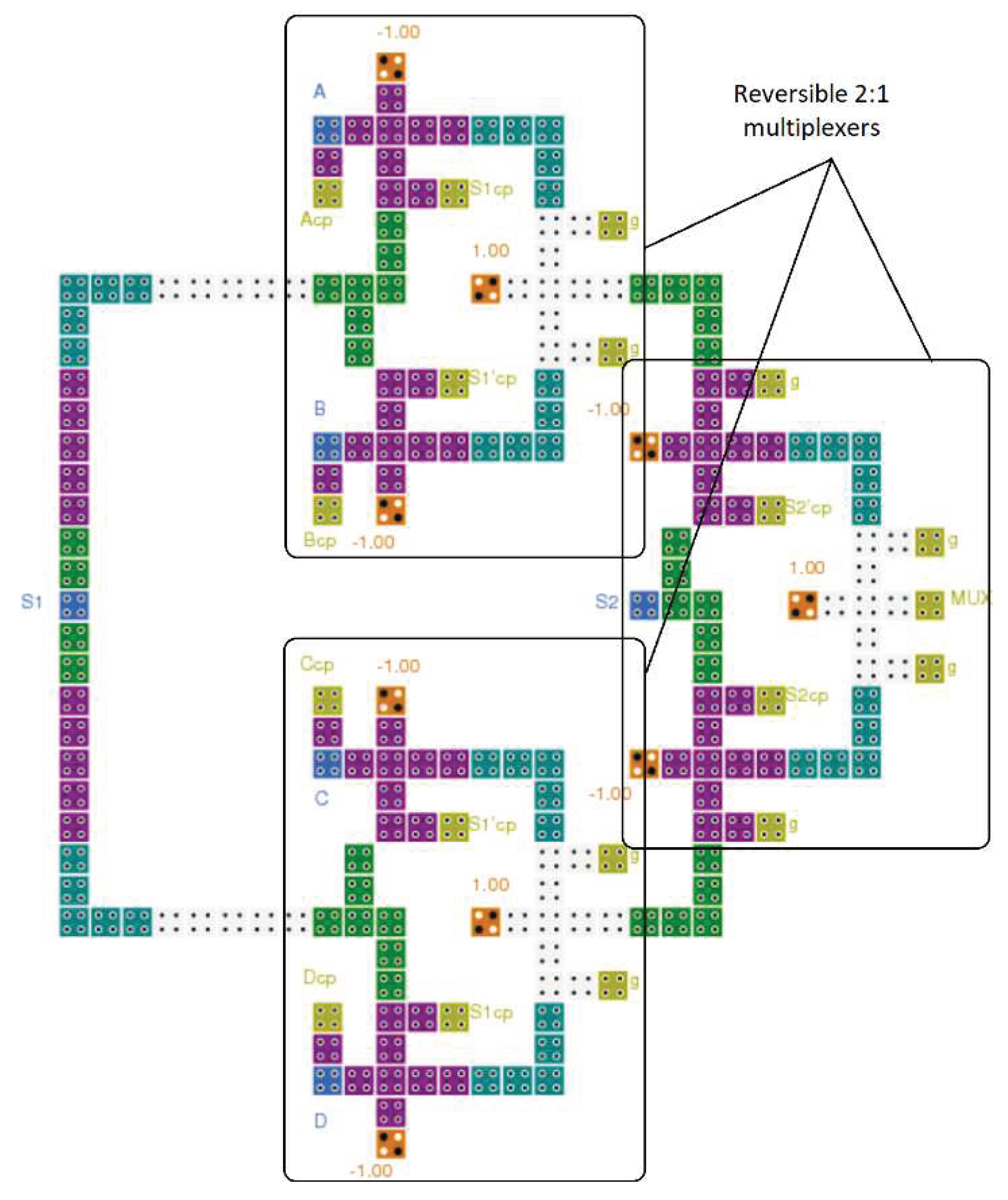
The circuit of a reversible QCA 4-to-1 multiplexer was built through the integration of three 2-to-1 multiplexers, as shown in
Figure 20. This circuit has a delay time of 12 clock zones (three clock cycles), requires 0.46 µm
2 of area, and uses a total of 213 QCA cells.
The proposed reversible QCA LU was created by combining three reversible QCA majority gates, a reversible QCA XOR, and a reversible QCA 4-to-1 multiplexer; see
Figure 21. It has a latency of 14 clock zones (3.5 clock cycles), costs 0.63 µm
2 of area, and requires 380 QCA cells to implement.
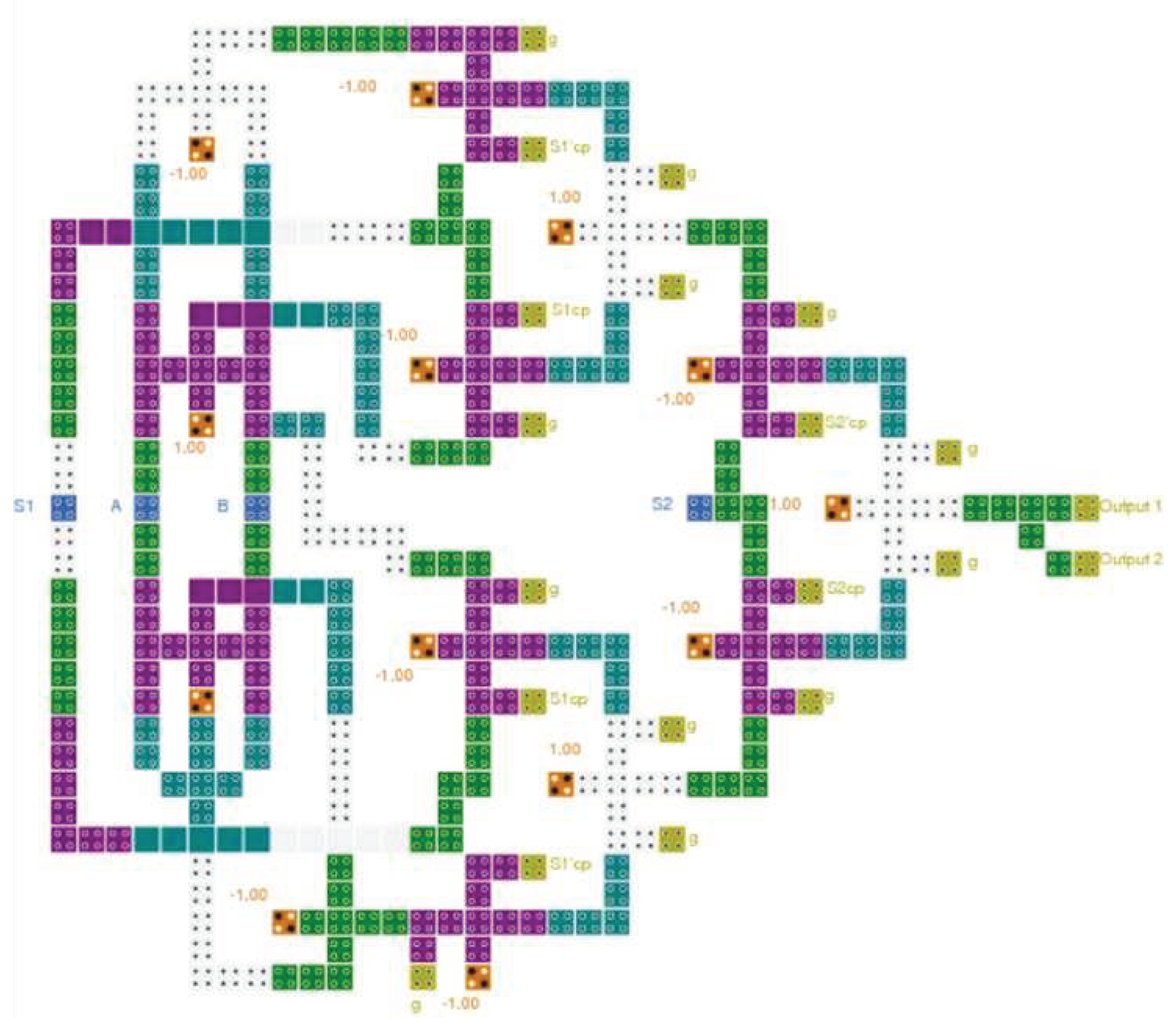
Figure 22 depicts the integration of two reversible QCA majority gates, a reversible QCA half-adder, a reversible QCA half-subtractor, and a reversible QCA 4-to-1 multiplexer to create the proposed reversible QCA AU. Its implementation requires 463 QCA cells, an area of 0.83 µm
2, and a delay of 14 clock zones (3.5 clock cycles).
For the development of reversible QCA CU, the reversible QCA 2-to-1 multiplexer, represented in
Figure 19, was used. The CU is crucial for selecting the ALU function, i.e., either an arithmetic or logical operation.
Finally, by combining the layout configurations of the three components LU, AU, and CU, and putting in the required QCA wiring lines, the novel reversible QCA ALU was completed, as illustrated in
Figure 23. The proposed reversible ALU implementation requires 1153 QCA cells, costs 2.14 µm
2 of area, and has a delay time of 24 clock zones (6 clock cycles).
6. Energy Dissipation Simulation Results and Discussion
Energy efficiency is the crucial benefit for designing digital circuits to be logically and physically reversible. The energy dissipation was calculated for each component of the proposed logically and physically reversible QCA ALU, including the reversible AND, OR, and XOR gates, as well as for the reversible half-adder, half-subtractor, 2-to-1 multiplexer, and 4-to-1 multiplexer circuits. In addition, the energy dissipation of the logically and physically reversible QCA LU, AU, and ALU was evaluated. The energy dissipation values are calculated using the
QCADesigner-E simulation tool.
Table 3 displays a summary of the energy dissipation analysis results. The simulation results demonstrated the exceptional energy efficiency achieved when designing QCA circuits using the physically and logically reversible design technique.
At a temperature of 1 K, every component, including the reversible AND, OR, and XOR gates, as well as the reversible half-adder, half-subtractor, 2-to-1 multiplexer, and 4-to-1 multiplexer circuits, exhibited exceptional energy dissipation values below the Landauer energy limit of kBTln2. Moreover, the proposed designs for a logically and physically reversible QCA LU, AU, and ALU possess ultralow energy dissipation with averages of 0.397 meV, 0.405 meV, and 0.908 meV per operation, respectively.
Table 4 compares our logically and physically reversible QCA ALU design to the most recent QCA ALU designs presented in the literature in terms of energy efficiency, number of operations, occupied area, required QCA cells, and latency. Additionally, this table presents the method used to deal with wire junctions as well as the reversibility status of each design. The logically and physically reversible QCA ALU design proposed in this study requires 1153 QCA cells, 2.14 µm
2 of area, and 6 clock cycles of delay to execute 16 operations. The multilayer crossover method, with three different layers, is used to prevent crosstalk interference between crossing wires.
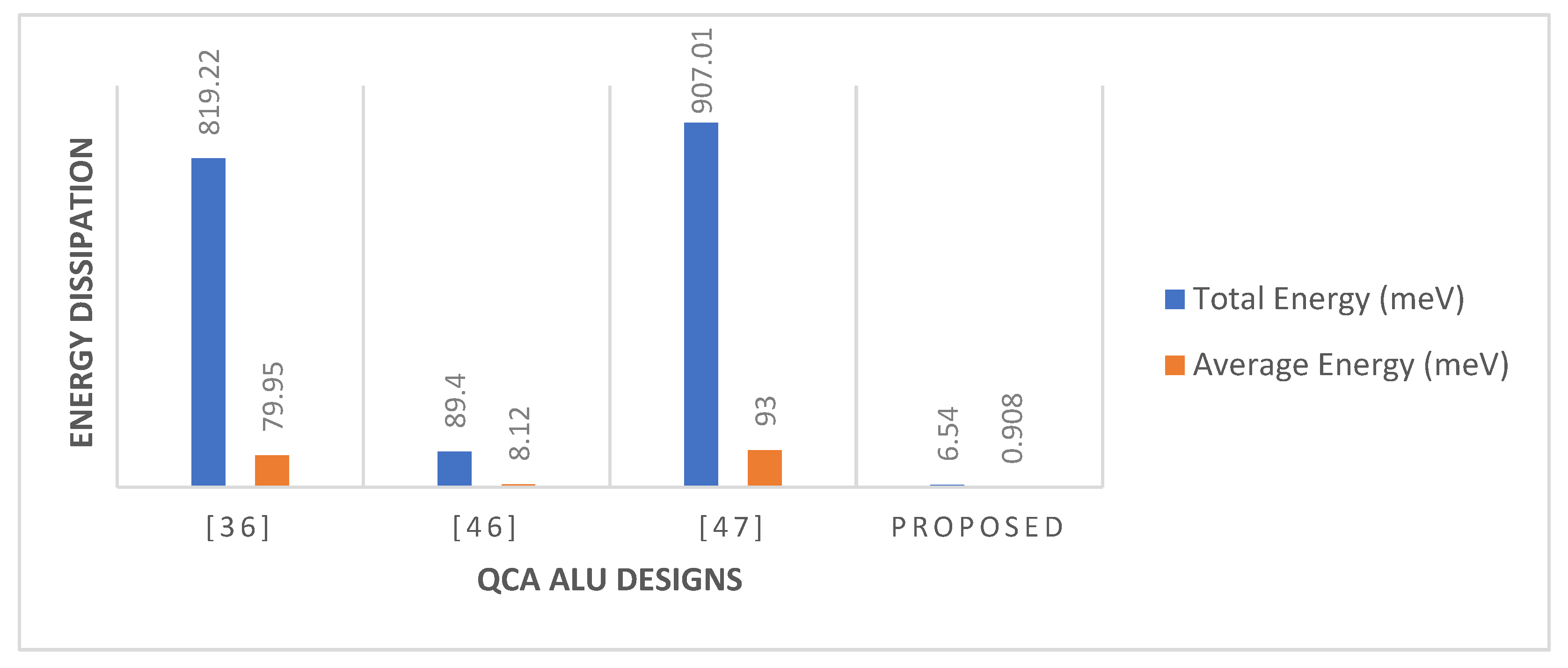
According to the simulation results, our proposed logically and physically reversible QCA ALU shows a significant reduction in energy dissipation compared with previous QCA ALU designs.
Figure 24 shows that the proposed QCA ALU consumes 88.8% less energy than the most energy-efficient QCA ALU designs proposed previously [
46].
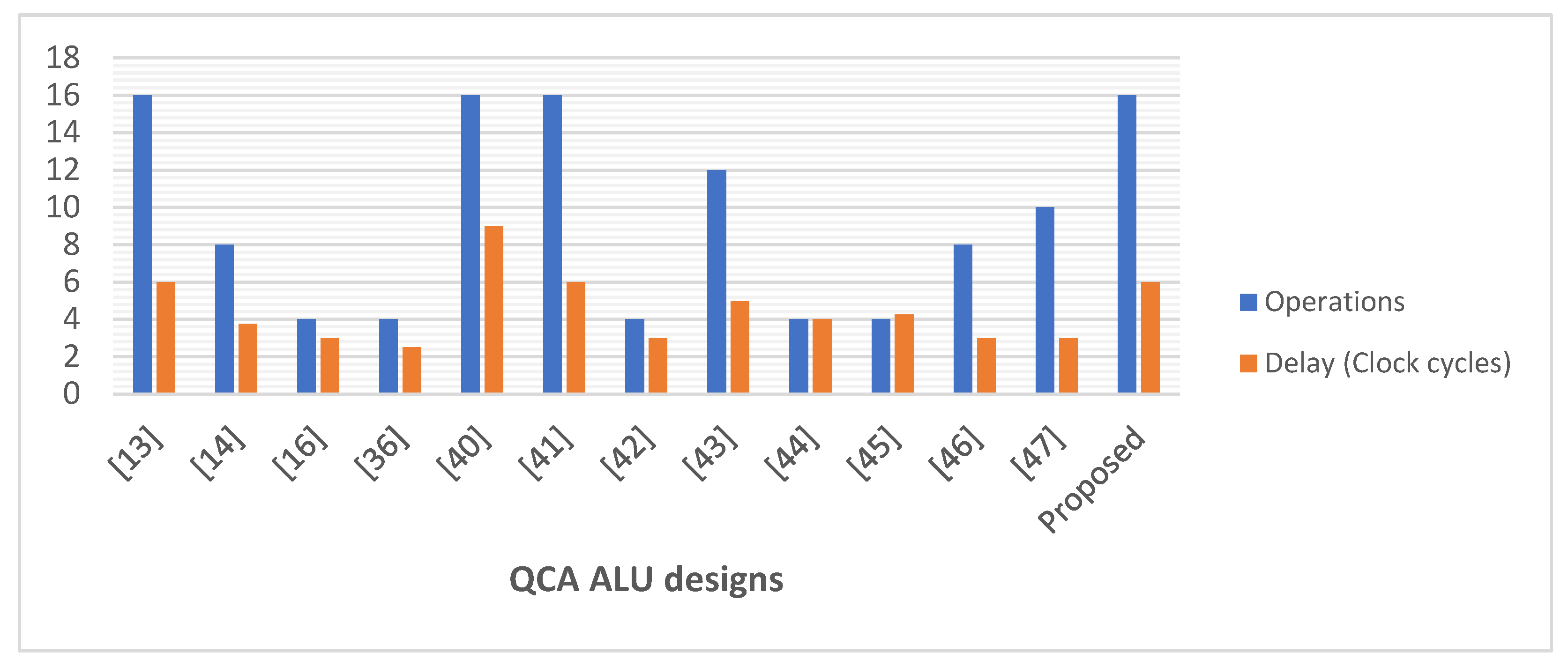
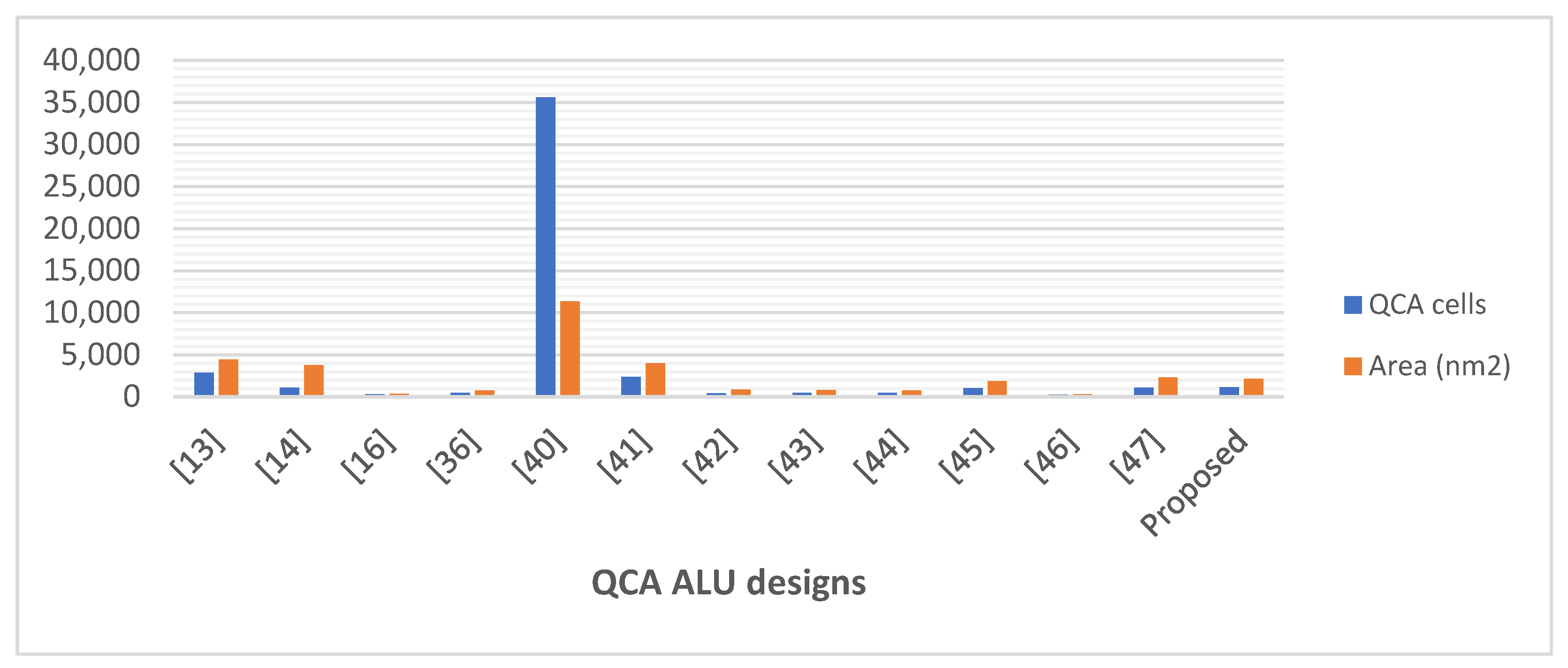
Figure 25 and
Figure 26 demonstrate the number of operations, delay time, occupied area, and required QCA cells for the novel logically and physically reversible QCA ALU design and the existing designs.
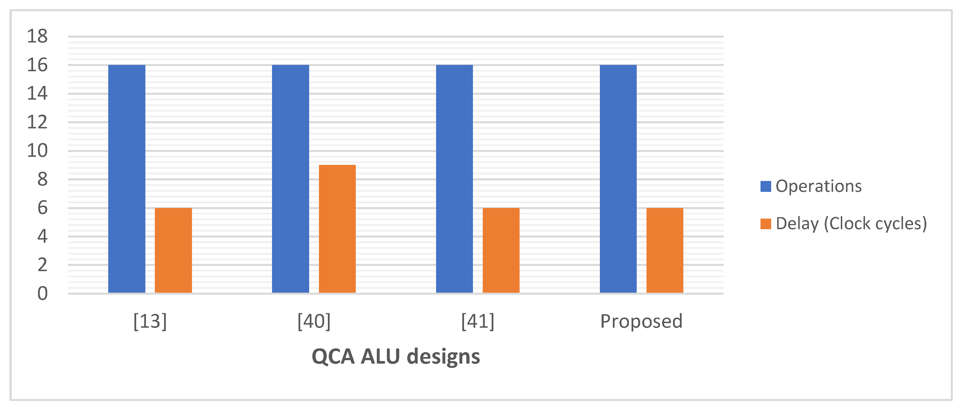
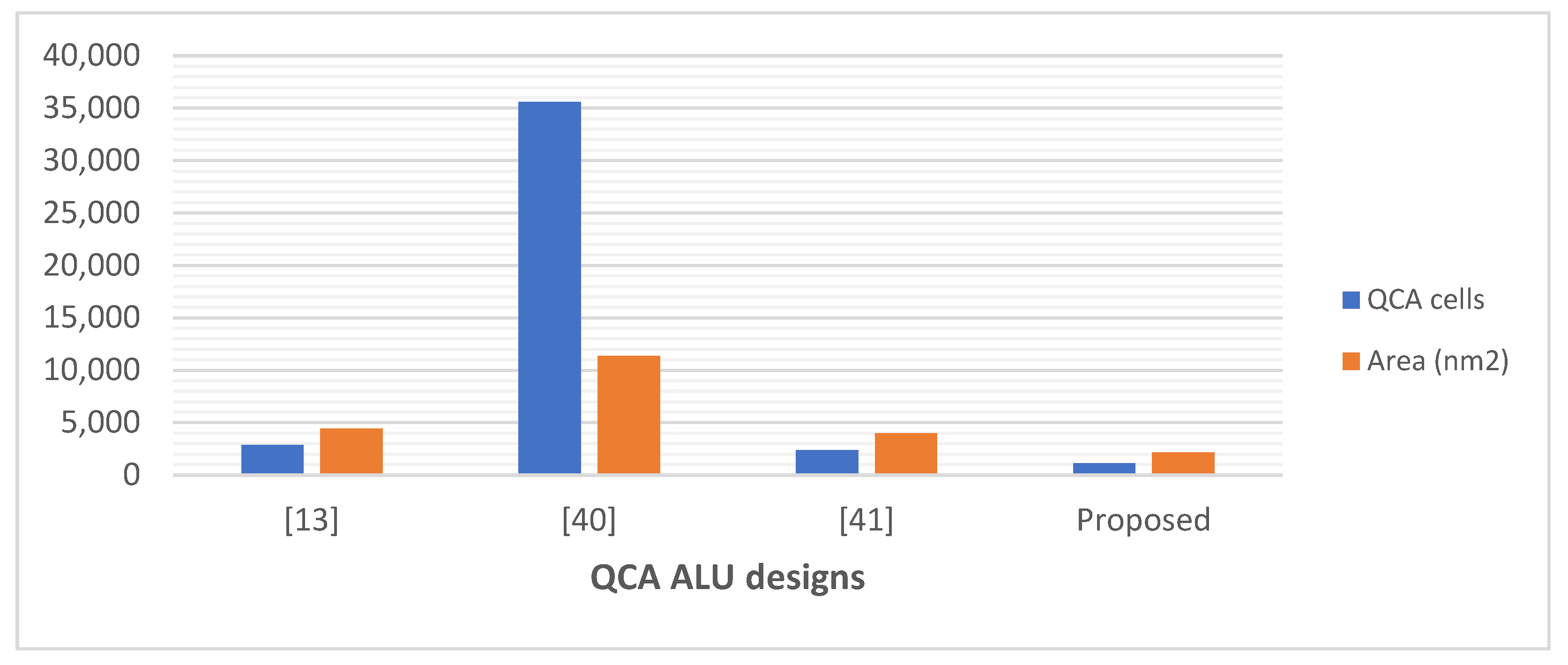
Although many previous designs utilized less area, QCA cells, and latency compared with the proposed ALU in this study, these ALUs performed fewer operations. Thus, for a more precise comparison, we compared our proposed ALU with QCA ALU designs that can perform a similar number of operations, as presented in
Figure 27 and
Figure 28. This comparison demonstrates that the logically and physically reversible design proposed in this study requires 51% fewer QCA cells, 47% less area, and a comparable latency compared to the best QCA ALU design previously presented that can perform 16 operations [
41].
7. Conclusion
The present work introduces a brand-new multilayer design of a logically and physically reversible QCA ALU with exceptionally low energy dissipation values, two orders of magnitude lower than other designs in the scientific literature. The fact that reversibility is maintained down to the layout level, which is the physical representation of the circuit, is the major advantage of this design. Theoretically, this means there is no longer any information loss, and as a result, no energy is being dissipated into the surrounding environment. In this research, we developed a building block majority gate that is both logically and physically reversible to create a QCA ALU with very low power consumption. The multilayer crossover method was used to prevent crosstalk interference between crossing wires. The USE clocking scheme was used to synchronize the data flow accurately and guarantee the correct operation of the ALU. The reversible QCA ALU presented here can perform sixteen distinct operations, half of which are logical and the other half arithmetic. The simulation of performance and the evaluation of energy dissipation was carried out using the QCADesigner-E program. To implement 16 operations, the logically and physically reversible QCA ALU design, proposed in this study, employs 1153 QCA cells, with an area of 2.14 µm2, and 6 clock cycles delay.
The simulation results confirmed that the energy dissipation values of the logically and physically reversible circuits used in the development of the proposed ALU were exceptionally small, below the Landauer energy limit of kBTln2. These circuits included reversible AND, OR, and XOR gates, as well as reversible half-adder, half-subtractor, 2-to-1 multiplexer, and 4-to-1 multiplexer circuits. Additionally, the findings from the simulation demonstrated that the proposed logically and physically reversible QCA ALU showed an improvement in energy efficiency by 88.8% compared with the recent design of M.Patidar et al. J. Supercomput. 2023. In addition, when compared to the most efficient 16-operation QCA ALU designs that were presented before, this ALU design utilizes 51% fewer QCA cells and 47% less area than the other designs.
In the future, the current proposed logically and physically reversible QCA ALU design can be extended to handle more operations. In addition, it can be expanded to the situation of ultra-energy-efficient multiple-bit ALU circuits.
Figure 1.
QCA cell polarization.
Figure 1.
QCA cell polarization.
Figure 2.
Adiabatic pipelining phases.
Figure 2.
Adiabatic pipelining phases.
Figure 3.
The USE clocking scheme (squares represent clock zones, and arrows show data flow).
Figure 3.
The USE clocking scheme (squares represent clock zones, and arrows show data flow).
Figure 4.
Logically and physically reversible QCA circuit design methodology.
Figure 4.
Logically and physically reversible QCA circuit design methodology.
Figure 5.
(a) Logical synthesis design of the standard irreversible majority gate, (b) physical layout design of the standard irreversible QCA majority gate.
Figure 5.
(a) Logical synthesis design of the standard irreversible majority gate, (b) physical layout design of the standard irreversible QCA majority gate.
Figure 6.
(a) Logical synthesis design of the eversible majority gate, (b) physical layout design of the reversible QCA majority gate.
Figure 6.
(a) Logical synthesis design of the eversible majority gate, (b) physical layout design of the reversible QCA majority gate.
Figure 7.
(a) Coplanar crossover method, (b) multilayer crossover method.
Figure 7.
(a) Coplanar crossover method, (b) multilayer crossover method.
Figure 8.
Block diagram of the proposed reversible QCA ALU.
Figure 8.
Block diagram of the proposed reversible QCA ALU.
Figure 9.
The synthesis of the proposed reversible LU (Acp and Bcp refer to copies of the inputs).
Figure 9.
The synthesis of the proposed reversible LU (Acp and Bcp refer to copies of the inputs).
Figure 10.
The synthesis of the proposed reversible AU (Acp and Bcp refer to copies of the inputs).
Figure 10.
The synthesis of the proposed reversible AU (Acp and Bcp refer to copies of the inputs).
Figure 11.
The synthesis of the proposed reversible XOR (Acp, Bcp, A’cp, and B’cp refer to copies of the inputs, and g1 and g2 indicate so-called garbage outputs).
Figure 11.
The synthesis of the proposed reversible XOR (Acp, Bcp, A’cp, and B’cp refer to copies of the inputs, and g1 and g2 indicate so-called garbage outputs).
Figure 12.
The synthesis of the proposed reversible half-adder (Acp, Bcp, A’cp, and B’cp refer to copies of the inputs, and g1 and g2 indicate so-called garbage outputs).
Figure 12.
The synthesis of the proposed reversible half-adder (Acp, Bcp, A’cp, and B’cp refer to copies of the inputs, and g1 and g2 indicate so-called garbage outputs).
Figure 13.
The synthesis of the proposed reversible half-subtractor (Acp, Bcp, A’cp, and B’cp refer to copies of the inputs, and g1 and g2 indicate so-called garbage outputs).
Figure 13.
The synthesis of the proposed reversible half-subtractor (Acp, Bcp, A’cp, and B’cp refer to copies of the inputs, and g1 and g2 indicate so-called garbage outputs).
Figure 14.
The synthesis of the proposed reversible 4:1 multiplexer (Acp, Bcp, S1cp, S2cp, S1’cp, and S2’cp refer to copies of the inputs, and g variables indicate so-called garbage outputs).
Figure 14.
The synthesis of the proposed reversible 4:1 multiplexer (Acp, Bcp, S1cp, S2cp, S1’cp, and S2’cp refer to copies of the inputs, and g variables indicate so-called garbage outputs).
Figure 15.
The synthesis of the proposed reversible 2:1 multiplexer (Acp, Bcp, S0cp, and S0’cp refer to copies of the inputs, and g1 and g2 indicate so-called garbage outputs).
Figure 15.
The synthesis of the proposed reversible 2:1 multiplexer (Acp, Bcp, S0cp, and S0’cp refer to copies of the inputs, and g1 and g2 indicate so-called garbage outputs).
Figure 16.
The layout of the proposed reversible QCA XOR (Acp and Bcp refer to copies of the inputs, and g1 and g2 indicate so-called garbage outputs).
Figure 16.
The layout of the proposed reversible QCA XOR (Acp and Bcp refer to copies of the inputs, and g1 and g2 indicate so-called garbage outputs).
Figure 17.
The layout of the proposed reversible QCA half-adder (Acp and Bcp refer to copies of the inputs, and g1 and g2 indicate so-called garbage outputs).
Figure 17.
The layout of the proposed reversible QCA half-adder (Acp and Bcp refer to copies of the inputs, and g1 and g2 indicate so-called garbage outputs).
Figure 18.
The layout of the proposed reversible QCA half-subtractor (Acp and Bcp refer to copies of the inputs, and g1 and g2 indicate so-called garbage outputs).
Figure 18.
The layout of the proposed reversible QCA half-subtractor (Acp and Bcp refer to copies of the inputs, and g1 and g2 indicate so-called garbage outputs).
Figure 19.
The layout of the proposed reversible QCA 2-to-1 multiplexer (Acp, Bcp, Scp, and S’cp refer to copies of the inputs, and g1 and g2 indicate so-called garbage outputs).
Figure 19.
The layout of the proposed reversible QCA 2-to-1 multiplexer (Acp, Bcp, Scp, and S’cp refer to copies of the inputs, and g1 and g2 indicate so-called garbage outputs).
Figure 20.
The layout of the proposed reversible QCA 4-to-1 multiplexer (Acp, Bcp, Ccp, Dcp, S1cp, S1’cp, S2cp, and S2’cp refer to copies of the inputs, and g variables indicate so-called garbage outputs).
Figure 20.
The layout of the proposed reversible QCA 4-to-1 multiplexer (Acp, Bcp, Ccp, Dcp, S1cp, S1’cp, S2cp, and S2’cp refer to copies of the inputs, and g variables indicate so-called garbage outputs).
Figure 21.
The layout of the proposed reversible QCA LU (S1cp, S1’cp, S2cp, and S2’cp refer to copies of the inputs, and g variables indicate so-called garbage outputs).
Figure 21.
The layout of the proposed reversible QCA LU (S1cp, S1’cp, S2cp, and S2’cp refer to copies of the inputs, and g variables indicate so-called garbage outputs).
Figure 22.
The layout of the proposed reversible QCA AU (Acp, Bcp, S1cp, S1’cp, S2cp, and S2’cp refer to copies of the inputs, and g variables indicate so-called garbage outputs).
Figure 22.
The layout of the proposed reversible QCA AU (Acp, Bcp, S1cp, S1’cp, S2cp, and S2’cp refer to copies of the inputs, and g variables indicate so-called garbage outputs).
Figure 23.
The layout of the proposed reversible QCA ALU (Acp, Bcp, Ccp, Dcp, S1cp, S1’cp, S1cp, S1’cp, S2cp, and S2’cp refer to copies of the inputs, and g variables indicate so-called garbage outputs).
Figure 23.
The layout of the proposed reversible QCA ALU (Acp, Bcp, Ccp, Dcp, S1cp, S1’cp, S1cp, S1’cp, S2cp, and S2’cp refer to copies of the inputs, and g variables indicate so-called garbage outputs).
Figure 24.
Energy dissipation comparison of QCA ALU designs.
Figure 24.
Energy dissipation comparison of QCA ALU designs.
Figure 25.
Number of operations and delay time of the QCA ALU designs.
Figure 25.
Number of operations and delay time of the QCA ALU designs.
Figure 26.
Occupied area and number of QCA cells used for designing the QCA ALUs.
Figure 26.
Occupied area and number of QCA cells used for designing the QCA ALUs.
Figure 27.
Number of operations and delay time of the QCA ALU designs that perform 16 operations.
Figure 27.
Number of operations and delay time of the QCA ALU designs that perform 16 operations.
Figure 28.
Occupied area and number of QCA cells used for designing the QCA ALUs that perform 16 operations.
Figure 28.
Occupied area and number of QCA cells used for designing the QCA ALUs that perform 16 operations.
Table 1.
Technology and simulation parameters used.
Table 1.
Technology and simulation parameters used.
| Parameter |
Description |
Value |
| QD size |
Quantum-dot size |
5 nm |
| Cell area |
Dimensions of each cell |
18 x 18 nm |
| Cell distance |
Distance between two cells |
2 nm |
| Layer separation |
Distance between QCA layers in multilayer crossing |
11.5 nm |
| Clock high |
Max. saturation energy of clock signal |
9.8E-22 J |
| Clock low |
Min. saturation energy of clock signal |
3.8E-23 J |
| Relative permittivity |
Relative permittivity of material for QCA system (GaAs & AlGaAs) |
12.9 |
| Radius of effect |
Maximum distance between cells whose interaction is considered |
80 nm |
| Temp |
Operating temperature |
1 K |
| τ |
Relaxation time |
1E-15 s |
| Tγ |
Period of the clock signal |
1E-9 s |
| Tin |
Period of the input signals |
1E-9 s |
| Tstep |
Time interval of each iteration step |
1E-16 s |
| Tsim |
Total simulation time |
8E-9 s |
| γshape |
Shape of clock signal slopes |
GAUSSIAN |
| γslope |
Rise and fall time of the clock signal slopes |
1E-10 s |
Table 2.
The operations of the proposed reversible QCA ALU.
Table 2.
The operations of the proposed reversible QCA ALU.
| Operation type |
Control inputs |
Output 1 |
Output 2
(Inversion of output 1) |
| S0
|
S1
|
S2
|
| Logic operations (LU) |
0 |
0 |
0 |
AND |
NAND |
| 0 |
0 |
1 |
OR |
NOR |
| 0 |
1 |
0 |
Buffer |
NOT (Inverter) |
| 0 |
1 |
1 |
XOR |
XNOR |
| Arithmetic operations (AU) |
1 |
0 |
0 |
A+B |
1’Complement (A+B)’ |
| 1 |
0 |
1 |
Cout
|
A.B |
| 1 |
1 |
0 |
A’.B |
(A’B)’ |
| 1 |
1 |
1 |
A-B |
(A-B)’ |
Table 3.
Energy dissipation analysis of the proposed reversible QCA ALU.
Table 3.
Energy dissipation analysis of the proposed reversible QCA ALU.
| Proposed logically and physically reversible QCA circuit |
Total energy dissipation (meV) |
Average energy dissipation (meV) |
| Reversible AND |
0.009 |
0.002 |
| Reversible OR |
0.009 |
0.002 |
| Reversible XOR |
0.054 |
0.014 |
| Reversible half-adder |
0.099 |
0.025 |
| Reversible half-subtractor |
0.063 |
0.016 |
| Reversible 4:1 multiplexer |
0.525 |
0.057 |
| Reversible CU (Reversible 2:1 multiplexer) |
0.112 |
0.014 |
| Reversible LU |
2.28 |
0.397 |
| Reversible AU |
2.84 |
0.405 |
| Reversible ALU |
6.54 |
0.908 |
Table 4.
Comparison of performance and energy dissipation. Note that there are only three references [
36,
46,
47] that calculate the energy dissipation for the QCA ALU.
Table 4.
Comparison of performance and energy dissipation. Note that there are only three references [
36,
46,
47] that calculate the energy dissipation for the QCA ALU.
| Reference |
Operations |
QCA cells |
Area (nm2) |
Delay (Clock cycles) |
Wire crossing |
Total energy dissipation (meV) |
Average energy dissipation (meV) |
Reversibility |
| [13] |
16 |
2,857 |
4,440 |
6 |
Coplanar |
NG |
NG |
Logically |
| [14] |
8 |
1097 |
3,740 |
3.75 |
Multilayer |
NG |
NG |
Logically |
| [16] |
4 |
332 |
380 |
3 |
Multilayer |
NG |
NG |
Logically |
| [36] |
4 |
452 |
740 |
2.5 |
Coplanar |
819.22 |
79.95 |
Irreversible |
| [40] |
16 |
35,596 |
11,370 |
9 |
Coplanar |
NG |
NG |
Irreversible |
| [41] |
16 |
2,370 |
4,010 |
6 |
Coplanar |
NG |
NG |
Logically |
| [42] |
4 |
420 |
850 |
3 |
Multilayer |
NG |
NG |
Irreversible |
| [43] |
12 |
485 |
790 |
5 |
Multilayer |
NG |
NG |
Irreversible |
| [44] |
4 |
464 |
780 |
4 |
Multilayer |
NG |
NG |
Irreversible |
| [45] |
4 |
1,010 |
1,860 |
4.25 |
Coplanar |
NG |
NG |
Irreversible |
| [46] |
8 |
231 |
280 |
3 |
Multilayer |
89.40 |
8.12 |
Irreversible |
| [47] |
10 |
1,069 |
2,340 |
3 |
Coplanar |
907.01 |
93.00 |
Logically |
| Proposed |
16 |
1,153 |
2,140 |
6 |
Multilayer |
6.54 |
0.908 |
Logically & physically |
