Preprint
Article

Cross-Mesh Clock Network Synthesis

This version is not peer-reviewed.

Submitted:

21 July 2023

Posted:

25 July 2023

You are already at the latest version

A peer-reviewed article of this preprint also exists.

Abstract
In the clock network design, the trade-off between power consumption and timing closure is an important and difficult issue. To achieve this target, a hybrid clock network architecture that combines both clock tree and clock mesh seems to be a promising solution. In this paper, we propose a novel clock mesh architecture – cross-mesh, with the average dispersion of the overall driving force, our methodology creates small non-zero skew clock trees. In addition, we integrate clock gating and register clustering techniques to further reduce dynamic power consumption. The proposed algorithms have four stages: cross-mesh planning, register clustering, mesh line connecting, and load balancing. Experimental results show that our methodology and algorithms get feasible solution effectively and improve both power consumption and clock skew simultaneously.
Keywords: 
Subject: 
Engineering  -   Electrical and Electronic Engineering

1. Introduction

In the design of a synchronous circuit, clock signal ideally must propagate to all components at the same time. However, since the distance from clock source to all sequential elements is different, there exists timing difference between these clock signal paths. A circuit with a large clock skew will cause the failure of its functionality. With the increasing complexity of high-performance chip design and process variation, clock network synthesis becomes a crucial and difficult problem.
There are three important issues in modern clock network synthesis problem: clock skew, process variation, and power consumption. To satisfy these considerations, clock tree and clock mesh are the two commonly used clock network synthesis approaches. Comparing these two approaches, clock tree network has shorter wire length and better power consumption, but it is more difficult to achieve timing closure and has less tolerance for process variation. On the other hand, clock mesh network has higher tolerance for process variation and is easier to satisfy the clock skew constraint, but it usually has much more power consumption.
Because of tightly clock skew constraint, process variation tolerance, and low power requirement in high performance circuit design, the concept of hybrid clock network was proposed in recent years. This style of clock network architecture aims at integrating both lower power advantage of clock tree and easy timing convergence of clock mesh, while achieving timing closure and optimizing power consumption.
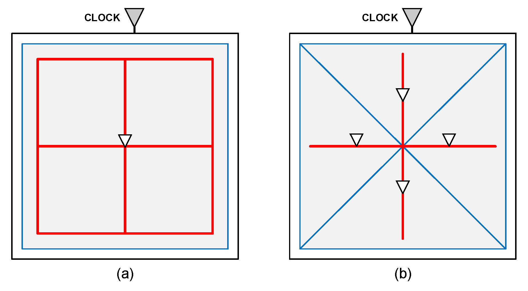
In this paper, we proposed a new cross-mesh architecture. In normal hybrid mesh/tree structure, the clock mesh layout was based on the board shape, driving buffer was placed in the intersection of mesh lines. For example, Figure 1(a) is a 2 × 2 size uniform clock mesh design, in which the driver buffer was placed in the mesh line intersection to drive the registers within the mesh, and its driving range was as shown by the gray rectangle. In contrast, our proposed cross-mesh layout is as shown in Figure 1(b). The range of a driving buffer is changed from the original rectangular area to cut into four triangular areas. We use this mesh architecture to distribute the buffers to balance the overall switching capacitance, reducing the number of registers connected to a sub-tree, and the load capacitance of a buffer.
Comparison of the two clock mesh architectures in Figure 1 is illustrated below. We assume the capacitance and power consumption of every piece of wire is 1 pf capacitance unit and 1 pw, 1X buffer has 4 pf capacitance and 4 pw power consumption, and 4X buffer has 10 pf capacitance and 10pw power consumption. In this example, uniform clock mesh is composed of twelve nets and one 4X buffer, total power consumption is 12*1+10 = 22 pw, total capacitance is 12*1+10 = 22 pf.
On the other hand, cross clock mesh uses four buffers as driving buffers to drive the same size of area, and each driving buffer in average only drives triangle area surrounded by blue line which is equal to one-fourth of original area. This change can reduce the output capacitance of the driving buffer, and hence timing convergence will be easier.
There are four 1X buffers and 4 pieces of wire in the circuit. The total capacitance can be calculated as 4*1+4*4=20pf, and power consumption is 4*1+4*4=20pw. In this example, we show that cross-mesh has not only smaller capacitance but also less power consumption in comparison with uniform mesh.
In addition to the proposed new type of hybrid clock network architecture, we also propose a clock gating and register clustering algorithm to resolve both clock skew and power consumption problems, and an effective solution to overcome the various operating environment problem.
The rest of this paper is organized as follows. Section 2 describes related work on clock tree, clock mesh, and hybrid network. Section 3 illustrates our motivation for integrating cross-mesh architecture and clock gating in local clock tree with an example. In section 4, we propose a four stages methodology for hybrid cross-mesh synthesis, clock gating, and register clustering. Experimental results in Section 5 show the effect of integrating these optimization techniques. Finally, we draw the concluding remarks in Section 6.

2. Related Works

2.1. Clock Tree

Buffer insertion, buffer sizing, and wire sizing are the most common techniques for the minimization of clock skew in clock tree synthesis [1,2,3,4,5]. While on the multi-voltage mode designs, adjustable delay buffers (ADBs) insertion and value adjustment are commonly used to resolve the clock skew problem. Researches [6,7] proposed a linear-time algorithm to assign delay values of ADBs for clock skew optimization on all power modes. Researches [8,9] proposed complete solutions for clock skew optimization under multiple power modes, including minimum number of ADBs required, allocation of ADBs, and delay value assignment of each ADB in each power mode. In modern VLSI Design, on-chip-variation (OCV) becomes serious as the feature size shrinks continuously. Research [10] presents a practical industrial design methodology for minimizing the OCV-induced clock skew of top-level clock tree, the basic idea is to pre-place guide buffers for clock tree synthesis so that wire lengths of non-common paths can be reduced.
Besides the minimization of clock skew, reducing power consumption of clock network is another important issue, and clock gating is a widely used technique. The location of a clock gate and the number of registers it drives have large impact on both the power consumption and the clock signal delay. Research [11] proposed a clock gate splitting methodology to improve enable time and increase setup time region. Research [12] integrated splitting and merging techniques to find the optimum location of clock gates. Research [13] proposed a graph-based algorithm for the clock root gating problem. Research [14] proposed a clustering method to reduce the number of buffers and power consumption. Research [15] proposed a linear programming methodology to minimize power consumption, wire length, and timing slew simultaneously. Research [16] proposed an activity-driven clock tree design methodology, including a new tree structure and a corresponding design flow. Research [17] proposed a skew-window-based methodology to reduce the total hardware cost of ADBs and clock gates simultaneously. Research [18] presents a general activity-driven clock tree structure in which both AND gate and OR gate can be utilized at any node. Based on this general structure, an effective synthesis algorithm is proposed.

2.2. Clock Mesh

Most researches on clock mesh synthesis targeted reducing power consumption of stub wires, including wire length reduction, mesh size tuning, and non-uniform mesh size. Research [19] proposed ILP formulations for register clustering, registers on neighboring locations with similar switching activities are grouped into one cluster to reduce wire length. Research [20] also proposed an ILP solution to move registers more closed to mesh wires and hence reduce length of stub wires. Research [21] proposed a binary search algorithm to find the suitable mesh size under the constraints of mesh size and register displacement. Research [22] proposed a greedy algorithm that select the drive buffer location and size to reduce the overall drive buffer hardware cost, and research [23] proposed a clock mesh design with wire sizing optimization.
In contrast to the uniform mesh structure, non-uniform mesh can reduce both the length of mesh wires and stub wires by adjusting the position of mesh wires. Research [24] proposed a graph-based non-uniform mesh methodology to reduce power consumption by planning more mesh wires in critical timing paths, and fewer mesh wires in non-critical timing paths. Research [25] iteratively moving the position of mesh wires until the length of mesh wires and stub wires were minimized. Research [26] proposed binary LP formulations for clock mesh synthesis and register assignment such that the capacitance of registers and stub wires can be balanced. Research [27] proposed a methodology to reduce the switching capacitance by non-uniform clock mesh synthesis, clock gate insertion, and register clustering. Research [28] proposed an integer linear programming (ILP) approach to reduce the wire length of a non-uniform clock mesh under temperature constraints.

2.3. Hybrid Network

Hybrid network aims at integrating both the benefit of clock tree and clock mesh. In the research [29], various clock network architectures are introduced, in which the hybrid clock architecture is divided into two categories, namely the upper clock mesh with the local clock tree (MLT) and the upper clock tree with the local clock mesh (Top tree with local meshes, TLM). Research [30] hierarchically constructed a hybrid mesh/tree clock network structure consisting of overlying zero-skew clock meshes, with underlying zero-skew clock trees originating from the mesh nodes. Research [31] focuses on the performance and optimization of multisource CTS flow which applies a coarse mesh with local sub-trees. They proposed several heuristic approaches to improving the performance of multisource CTS, especially for skew optimization. In research [32], with a combination of non-uniform meshes and un-buffered trees, a variation-tolerant hybrid clock distribution network was produced. Clock skew variations were selectively reduced based on circuit timing information generated by static timing analysis. Research [33] proposed a hybrid method that creates a mesh upon a tree topology. A clock mesh was built first according to the positions and capacitance of the sinks. A top-level tree was then built to drive the mesh. A blockage-aware routing method is used during tree construction.
In this paper, we propose a novel clock mesh architecture – cross-mesh, with the average dispersion of the overall driving force, our methodology creates small non-zero skew clock trees and reduces the usage of clock gates. We also propose a clock gating and register clustering algorithm to resolve both clock skew and power consumption problems. Our algorithms have four stages: cross-mesh planning, register clustering, mesh line connecting, and load balancing. Experimental results show that our approach can get feasible solution and effectively improve power consumption and clock skew.

3. Motivation Example

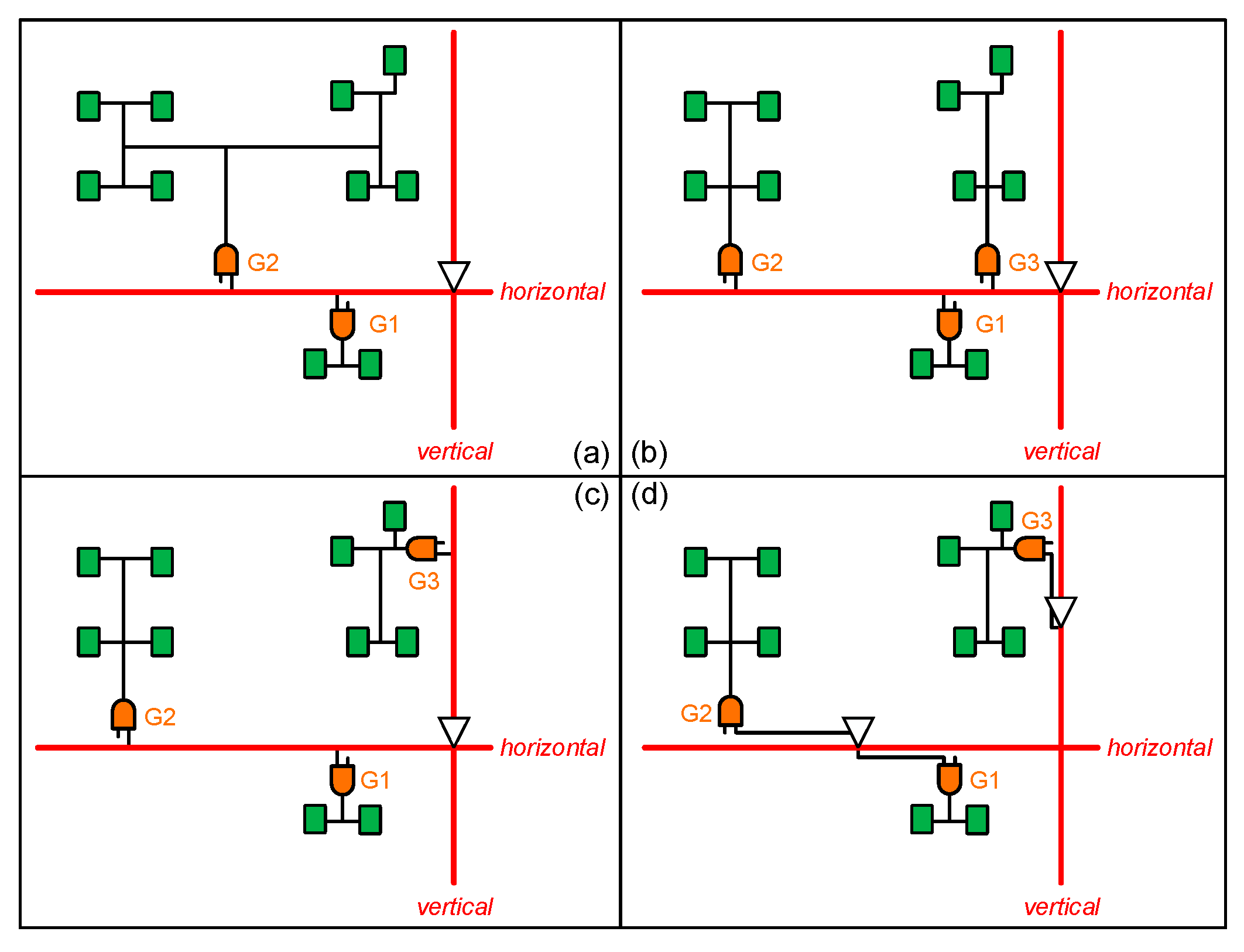
The example in Figure 1 illustrates how to take driving buffer and mesh wire into consideration, and the use of cross-mesh architecture to reduce total capacitance and power consumption. In this section, we further illustrate our motivation for integrating cross-mesh architecture and clock gating in local clock tree and analyze capacitance and power consumption of clusters in each kind of sub-tree topology with the example in Figure 2. Based on the circuit in Figure 2(a), Figure 2(b) and Figure 2(c) illustrate how clock gating and load balancing techniques can reduce capacitance load on mesh wires, Figure 2(d) illustrates how we integrate these two optimization methods with the cross-mesh architecture to further reduce capacitance load. Details of this example are described below.
The switching capacitance and power consumption of a cluster are defined as following formulas:
C a p t o t = C a p m e s h _ w i r e + α × ( C a p g a t e + C a p s u b t r e e w i r e + C a p r e g )
P w r t o t = P w r m e s h _ w i r e + α × P w r g a t e + P w r s u b t r e e _ w i r e + P w r r e g
Capmesh_wire is wire capacitance from driving buffer to the gate that is the beginning of a cluster, Capgate is the capacitance of cluster gate, Capsubtree_wire is the wire capacitance in a cluster, and Cap reg is the capacitance of register. Because we use clock gate to control a cluster, it needs a parameter α to represent the activity ratio of a cluster. If α = 0.5 , it means this cluster will activate half of time during working process. To simplify the problem, we assume α of every gate is 0.5 in this example. Note that parameters of power are similar to capacitance’.While for the other parameters, we assume the capacitance and power of 1X gate are 6 pf and 6 pw, and that of 4X gate are 14 pf and 14 pw. Similarly, we assume the capacitance and power of registers are 5 pf and 5 pw.
In Figure 2(a), circuit A is a conventional mesh tree which branches two clusters. For cluster 1, we assume Capmesh_wire = 5pf, Pwrmesh_wire = 5pw and Capsubtree_wire = 5pf, Pwrsubtree_wire = 5pw, therefore C a p t o t = 5 + 0.5 6 + 5 + 5 × 2 = 15.5 p f and P w r t o t = 15.5 p w . For cluster 2, we assume Capmesh_wire = 10pf, Pwrmesh_wire = 10pw and Capsubtree_wire = 30pf, Pwrsubtree_wire = 30pw, therefore C a p t o t = 10 + 0.5 14 + 30 + 5 × 8 = 52 p f and P w r t o t = 52 p w . In cluster 2, there are eight registers in the tree topology, thus it needs to use 4X gated cell to drive the clock tree. At last, the average capacitance is 33.75pf and total power consumption is 62.5pw. Incidentally, PWRmesh_wire1 is public in clusters 1 and 2, we only need to calculate one time in total power consumption.
Based on conventional mesh circuit, we can optimize circuit A by two ways. For the first optimization method, because cluster 2 is too large to drive by a gate, we insert another gate G3 to divide cluster 2 into two smaller clusters by analyzing registers’ activity status like circuit B in Figure 2(b). The advantage of this method is that not only mitigate the capacitance of each gate (in other words, large gate can be instead by smaller one), but also increase the possibility of closing time due to more similarity between clusters. In circuit B, we assume Capmesh_wire and Pwrmesh_wire of clusters 1, 2, 3 as 5pf, 13pf, 4pf, and 5pw, 13pw, 4pw; Capsubtree_wire and Pwrsubtree_wire are 5pf, 13pf, 14pf, and 5pw, 13pw, 14pw. By formulas (1) and (2), we get Captot of clusters 1, 2, 3 are 15.5pf, 32.5pf, 24pf, and Pwrtot of clusters 1, 2, 3 are 15.5pw, 32.5pw, 24pw. The average capacitance of circuit B is 24pf and total power consumption is 63pf. This optimization in circuit B significantly reduce average capacitance of driving gate but only have 0.5pw of cost increased.
The second optimization method aims at balancing gate amount on all mesh wires. Actually, it is better to put all gates on the mesh wires in average to reduce the maximum loading, since too much loading of mesh wire will induce timing as well as temperature problem in the circuit. For circuit C in Figure 2(c), we assume Capmesh_wire and Pwrmesh_wire of clusters 1, 2, 3 as 5pf, 13pf, 8pf, and 5pw, 13pw, 8pw; Capsubtree_wire and Pwrsubtree_wire are 5pf, 13pf, 14pf, and 5pw, 13pw, 14pw. By formulas (1) and (2), we get Captot of clusters 1, 2, 3 are 15.5pf, 32.5pf, 28pf and Pwrtot of clusters 1, 2, 3 are 15.5pw, 32.5pw, 28pw. The average capacitance of circuit C is 25.3pf and total power consumption is 71pw. Compare to circuit B, it has a little increase in both average capacitance and total power consumption. However, if we only focus on horizontal mesh wire, it gets better average capacitance and total power consumption as 24pf and 43pw due to cluster 3 is moved to y-axis mesh wire.
While circuit D in Figure 2(d) is different from the two previous methods, we use the proposed cross-mesh structure to build mesh tree. Despite circuit C balances the loading of mesh wires, the burden of driving buffers is still the same. To resolve this problem, our method put driving buffers on both x-axis mesh and y-axis mesh. It means that gate cell in the cluster will connect to the mesh tree in average by these guide buffers. We assume Capmesh_wire and Pwrmesh_wire of clusters 1, 2, 3 as 4pf, 5pf, 3pf, and 4pw, 5pw, 3pw; Capsubtree_wire and Pwrsubtree_wire are 5pf, 13pf, 14pf, and 5pfw 13pw, 14pw; Pwrmesh_wire of buffer12 and buffer3 are 8pw, 5pw. According to the formulas, we get Captot of clusters 1, 2, 3 are 14.5pf, 24.5pf, 23pf and Pwrtot of clusters 1, 2, 3 are 14.5pw, 24.5pw, 23pw. Because there are two driving buffers in the circuit, we analyze average capacitance and total power consumption for each buffer. For buffer12, average capacitance is 19.5pf and total power consumption is 47pw. On the other hand, average capacitance and total power consumption are 23pf and 28pw for buffer3. This result shows that our cross-mesh structure can further reduce capacitance of each cluster. We cannot compare power consumption between conventional mesh tree and cross-mesh tree here directly due to their different structure. Instead, we will discuss it in next paragraph with power consumption of whole mesh tree.
To compare average output capacitance to drive buffers and total power consumption of whole circuit between four results in Figure 2, we assume the power consumption of driving buffer is 4pw, and a piece of mesh wire is 18pw. According to mesh structure in Figure 1, there are twelve pieces of mesh wires in conventional mesh structure, and only four pieces of mesh wires in the cross-mesh structure. Since all circuits in Figure 2 only use one fourth of whole mesh circuit, thus we calculate circuit A to circuit C as four piece of mesh wires, and circuit D as two piece of mesh wires. In Table 1, Capavg in subtree denotes average capacitance of every cluster, while Capavg in whole circuit is the average output capacitance to each driving buffer, and Pwrtot is total power consumption of the whole circuit. In this table, we can see that cross-mesh structure has much better results than the three others.

4. Design Flow and Methodology

4.1. Overview

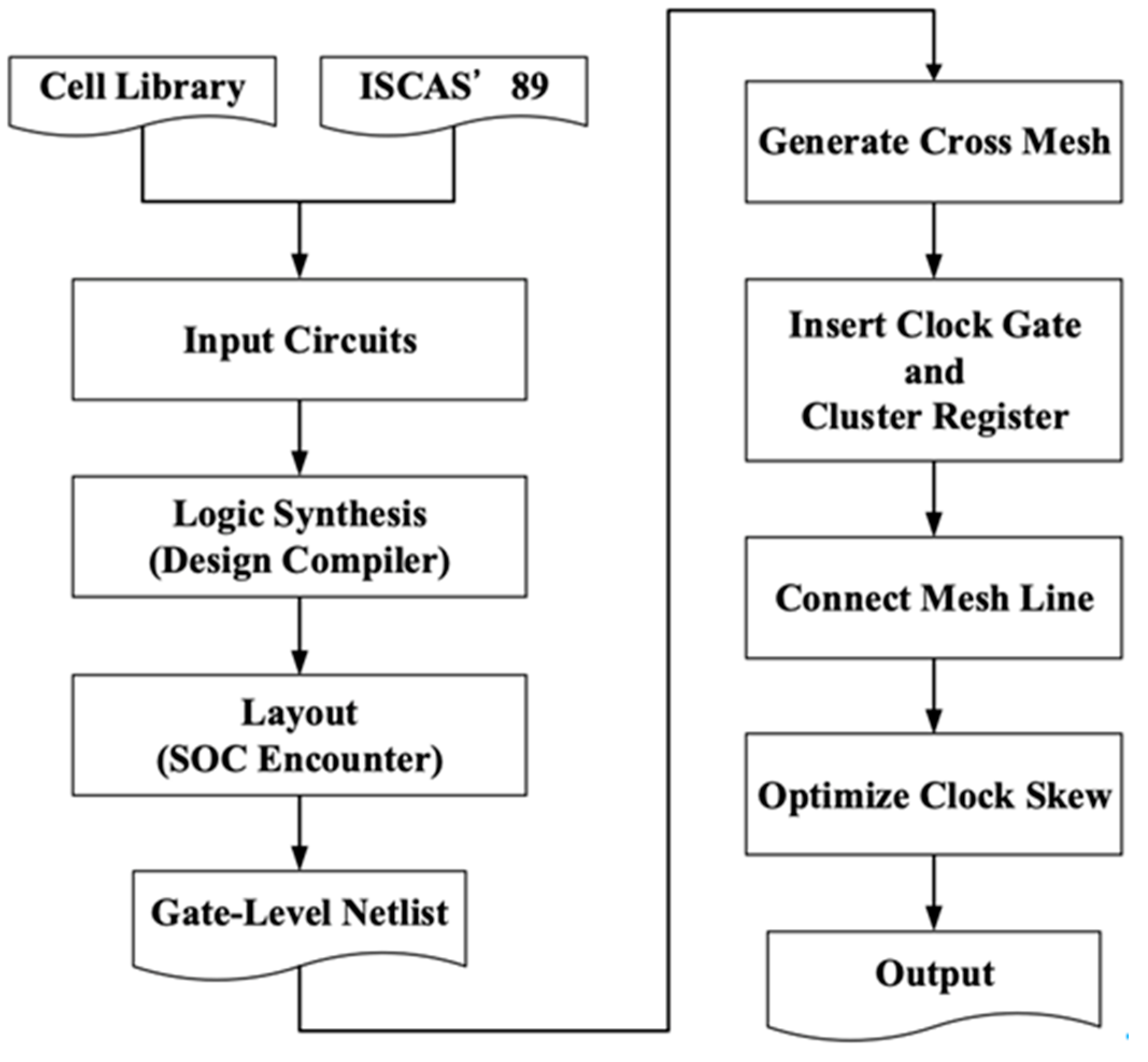
There are four stages in our proposed methodology. As shown in Figure 3, our program read post-placement circuit to help constructing cross-mesh tree. The first stage is cross-mesh construction and primary driving buffer placement, we classify registers into groups according to the buffer driving range. The second stage is to insert clock gate if necessary. We cluster registers into groups based on cluster constraint to optimize total capacitance, and decide size and location of logic gates, then insert them to control the clusters. After that, the relationship between clusters will be established, the third stage is to connect each clock sub-tree to the drive buffer until they become a completed mesh tree. Finally, the fourth stage is to balance the load capacitance of each clock sub-tree, we evaluate all branches of the mesh tree and balance their capacitance to further minimize clock skew between them. The detailed skill of each stage is illustrated in the following subsections.

4.2. Cross-Mesh Planning Algorithm

There are three steps in this stage: cross-mesh construction, driver buffer placement, and register classification. In the first step, we plan and construct cross-mesh by input file, which includes chip’s structure and cells’ location. After that, we place drive buffers to suitable locations in the chip. At last, our program assigns registers to its most fitting drive buffer according to area of drive buffers and location of registers.
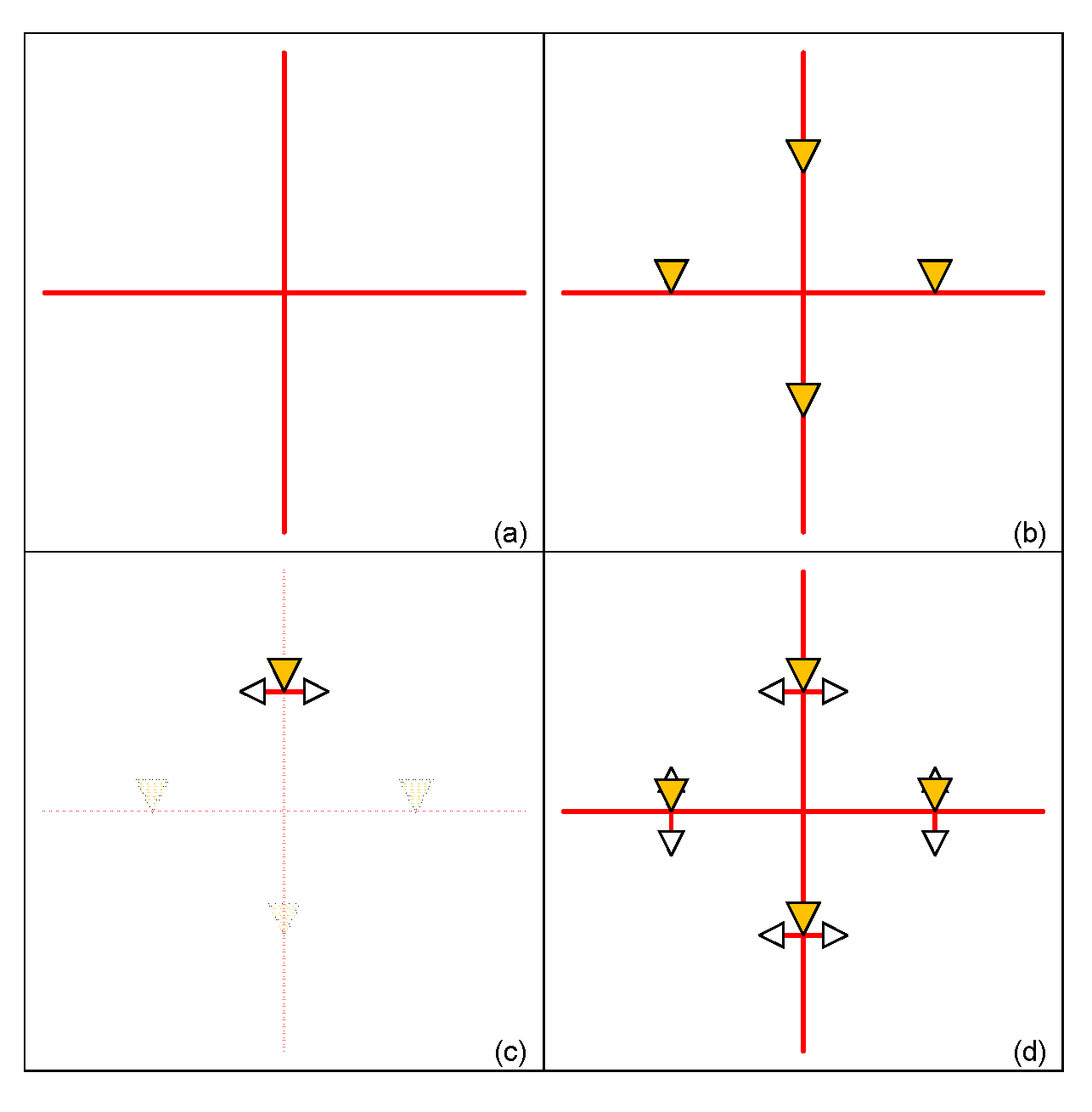
We use Figure 4 to illustrate our method, our program uses core size in the chip to determine how to setup mesh wire. The rectangle area of the core is represented by coordinates of left-bottom (Corex1, Corey1) corner and right-top corner (Corex2, Corey2). We use formulas (3), (4) to get coordinate of cross-mesh from core information.
C r o s s M e s h x = C o r e x 1 + C o r e x 2 2
C r o s s M e s h y = C o r e y 1 + C o r e y 2 2
In formula (3) and (4), Cross-Meshx and Cross-Meshy are coordinates of cross-mesh. After completing mesh wire construction, we start to insert drive buffers in mesh structure. For the example in Figure 4 (a), there are four directions of wire in the tree (red line). First, we put drive buffers on the center of every piece of mesh wire respectively (orange triangle) in Figure 4 (b). Mesh tree will use these four buffers to drive cells. Because the complexity of IC design grows drastically, it is insufficient to drive cross-mesh by only four drive buffers. We divide original triangle drive area in half by mesh wire like Figure 4 (c), adding two additional drive buffers (white triangle) to make up for inadequate of drive strength. The design with completed mesh structure is as shown Figure 4 (d).
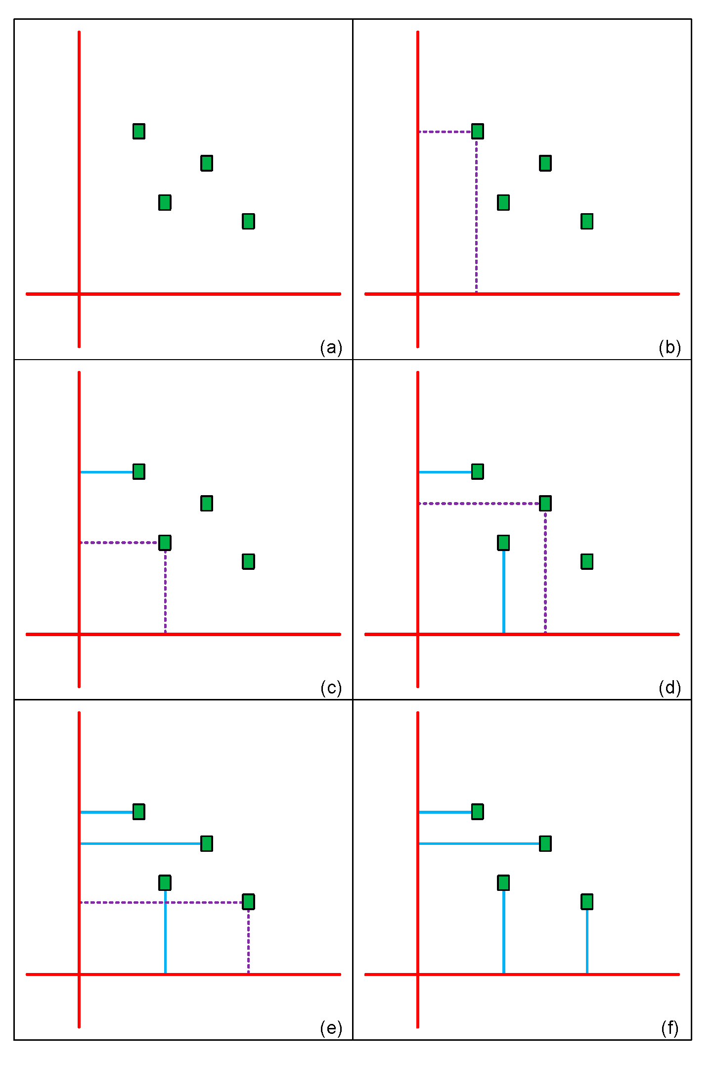
After the first two steps, the third step classifies registers and connects them to corresponding drive buffers. The standard of classification is the Manhattan distance from mesh wire to register. That is, we can get a guaranteed result that has smallest routing distance to reduce wire capacitance. We use Figure 5 (a) for the illustration example, this original circuit has a completed constructed mesh structure (red line) that has a horizontal wire and a vertical wire, and there are four free registers (green rectangle) need to be classified. In Figure 5 (b), we first choose a register to calculate and compare its distance to horizontal and vertical mesh wire (purple dotted line). Obviously, it is near to vertical mesh wire, thus the program assigns it to drive buffer on vertical mesh wire like blue line in Figure 5 (c). If register has the same distance to vertical and horizontal wire. In this case, we take the number of registers belonging to drive buffer to make a decision. The smaller one will be chosen. In Figure 5 (d), the other register is in this situation. The program assigns it to horizontal drive buffer due to the amount of it is zero. Note that if the number of belonging registers is the same. The program will appoint it randomly like Figure 5 (e). The program classifies registers by this method iteratively until whole registers all have their corresponding drive buffer in Figure 5 (f).

4.3. Register Clustering Algorithm

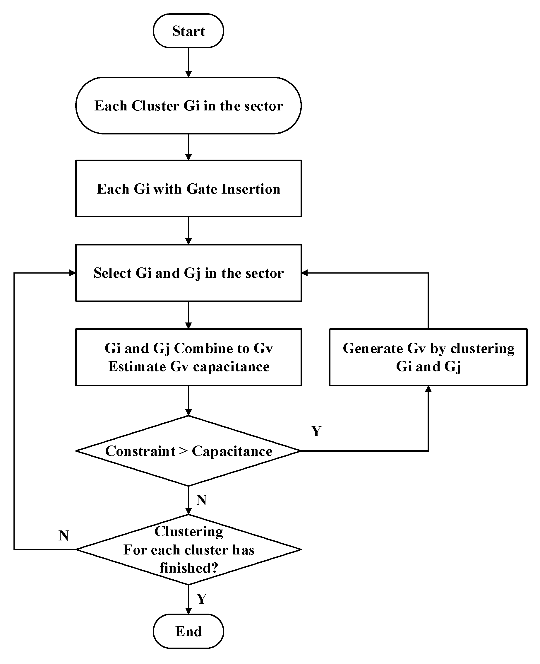
Despite the previous stage classifying registers to their suitable drive buffer roughly, the number of registers for each drive buffer is still too much. Therefore, clustering these registers to groups and inserting more buffers to drive them is imperative. Figure 6 is the flow graph of this stage. Firstly, we treat each register as an individual cluster, then our algorithm inserts a clock gate to each cluster. Note that we use the same type of clock gate in the optimization procedure to enhance the efficiency of following zero skew tree timing closure. Secondly, we use greedy-like algorithm to merge clusters. For example, assume clusters Gi and Gj which are neighbors are selected in the algorithm. If total capacitance of Gi and Gj is smaller than the limit of load capacitance, clusters Gi and Gj will merge as a new cluster Gv. This procedure continues until total capacitance is over threshold. With this method, we can group registers rapidly with good results and also satisfy design constraints.
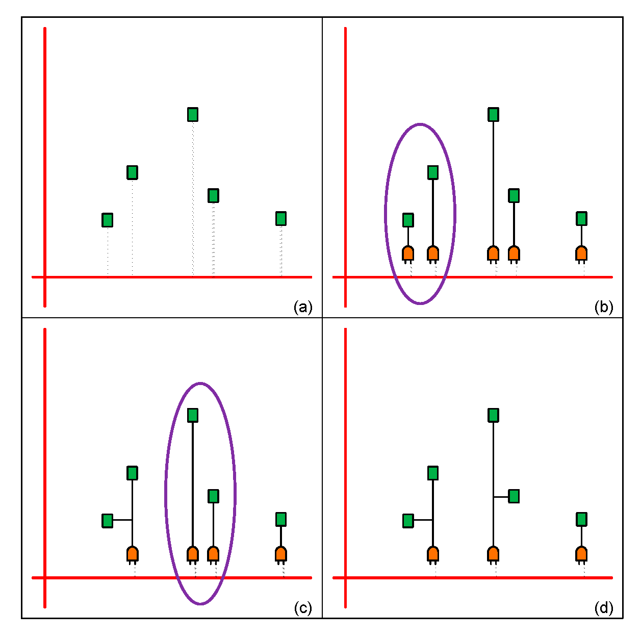
Figure 7 is an example of our algorithm, there are five registers in this area (green rectangle), red line represents mesh wire and grey line means these registers belong to horizontal mesh wire. In Figure 7 (a), the program first treats each register as a cluster and then inserts a clock gate for each cluster as shown in Figure 7 (b). After that, distance between pair of registers is sorted to make sure that merged clusters in the next step are neighbors. In Figure 7 (b), the two registers in purple circle are near each other and are the best candidates to choose. Hence, we merge them as a cluster like Figure 7 (c) and continue merging other clusters. Finally, we can group registers into three clusters as shown in Figure 7 (d). The optimization in this stage can not only reduce power consumption but also balance output capacitance. This stage plays an important role in our whole design flow since better clustering brings out a better clock mesh tree structure. In other words, good clustering not only has lower power consumption but also better timing closure achievement.

4.4. Mesh Network Connecting Algorithm

In this stage, we build whole clock mesh tree by connecting sub-tree we clustered in previous stage to drive buffer and inserting buffers between drive buffer and sub-tree if necessary. We use formula (5) to calculate the output capacitance of each drive buffer, where C w i r e is total wire capacitance from drive buffer to every clock gate; N G a t e i is the amount of all clock gates. C G a t e is the capacitance of a clock gate. If C o u t p u t _ l o a d is too large to a drive buffer, it means this group needs splitting to reduce capacitance. Thus, our algorithm will divide clusters into several groups and insert new buffers to help drive buffer driving all clusters in its area. We continue this step iteratively until its capacitance can be driven by a drive buffer.
C o u t p u t _ l o a d = C w i r e + i n N G a t e i × C G a t e
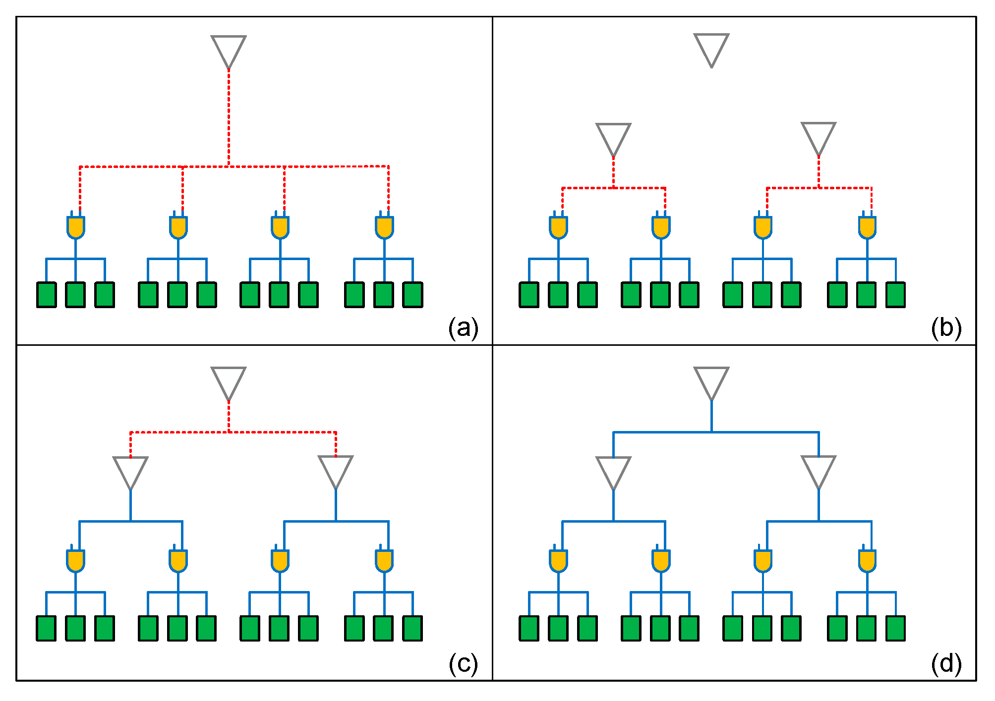
In Figure 8, we use an example to illustrate the mesh network connecting algorithm, there is a drive buffer (white triangle) and four cluster of registers as shown in Figure 8 (a). In the beginning, we connect four clusters to drive directivity, and therefore output capacitance is too large to the drive buffer. Hence, we divide a group to half and insert two drive buffers to help original drive buffer drive these clusters as shown in Figure 8 (b). Then our algorithm calculates their capacitance again as in Figure 8 (c), we find that these two new groups can all be driven by their drive buffer, and also the two new drive buffers can be driven by original drive buffer. Finally, we connect all buffers and clock gates as in Figure 8 (d). After this stage, clock mesh tree is established completely, but there still has design space to further optimize its timing issue as described in the next stage.

4.5. Load Balancing Algorithm

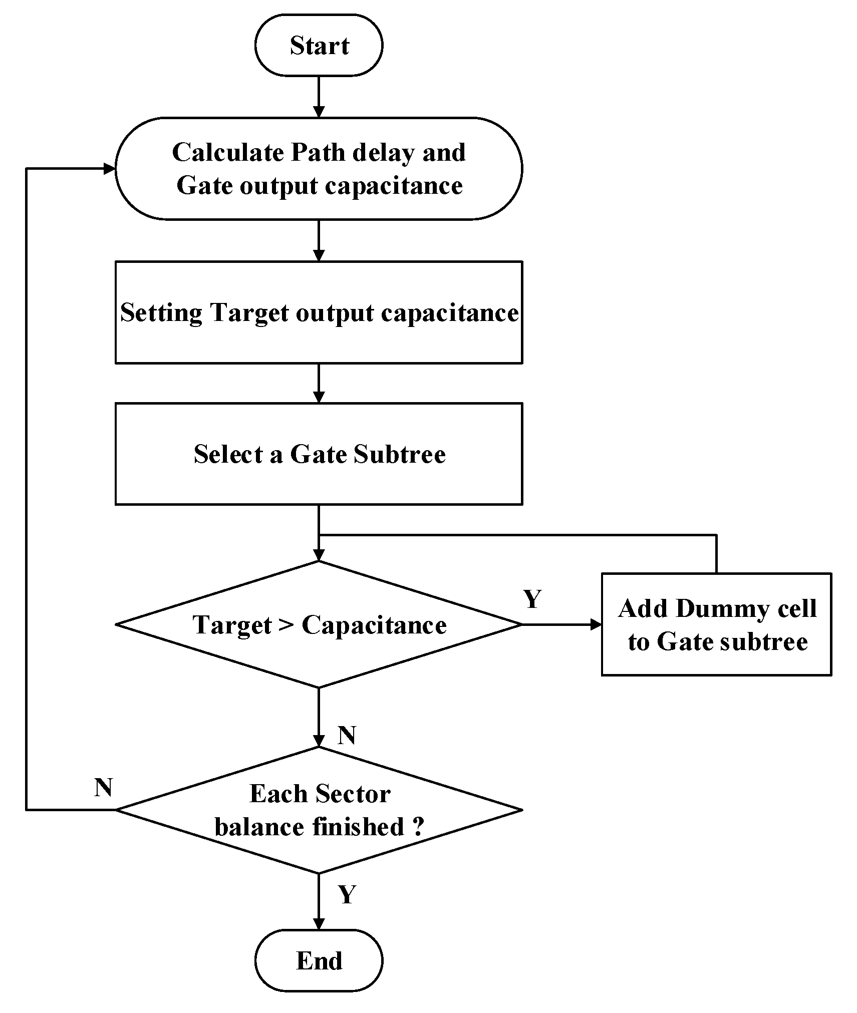
In this stage, we optimize the timing issue by two phases. The first phase is to optimize the timing difference of the clock gate subtrees. We use load matching technology to build the clock tree in order to make the clock skew close to zero. And to make the load capacitance in each clock gate subtree to be closer, we insert dummy cells to make the delay of clock gates to be consistent. Figure 9 shows the algorithm of balancing the load capacitance of the clock gate subtree. In the beginning, we first calculate the path delay and capacitance before optimization, find the clock gate subtree with the largest capacitance value, and set its capacitance value as the target capacitance value. Then, we select each clock gate subtree in order and compare its capacitance with the target capacitance value. If it is less than the target capacitance value, we calculate the difference and estimate how many dummy cells are needed to reach the target capacitance. The formulas are as follows:
N d u m m y = C t a r g e t C b e f o r e / C d u m m y
C e x t r a = C d u m m y × N d u m m y
C a f t e r = C b e f o r e + C E x t r a
Formula (6) is to calculate the number of required dummy cells N_dummy, where C_target is the target capacitance, C_before represents the clock gate load capacitance that has not insert dummy cells, and C_dummy is the capacitance value of dummy cell. The additional capacitance value C_extra is calculated by formula (7), and the load capacitance of the clock gate subtree is updated by formula (8). These steps are repeated until all the clock subtree load capacitances are updated.
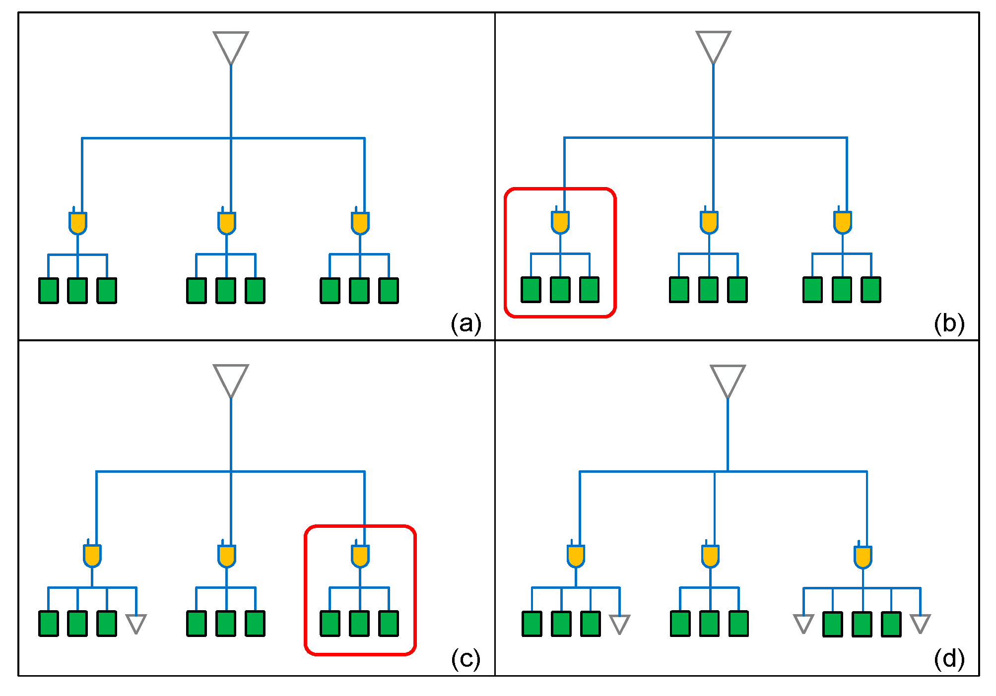
The example in Figure 10 is a schematic diagram of a drive buffer connecting three clock gate subtrees. After calculating the load capacitance of each subtree, assume the middle clock subtree in Figure 10 (a) has the maximum load capacitance, we set this capacitor value as the target limit, and then add the redundant components one by one. In Figure 10 (b), we first process the left clock subtree and calculate the number of components added according to the above three formulas. As shown in Figure 10 (c), adding a redundant component to the left subtree can match the value of the target capacitor, and then processing the clock subtree on the right. We repeat this method to add redundant components until all clock subtrees are processed as shown in Finally, Figure 10 (d).
After the first stage of optimization is completed, we enter the second stage of load balancing between the secondary buffers on mesh lines. This procedure is similar to that of the previous stage. We calculate the load capacitance of all the secondary driver buffers and set the maximum value as the target capacitance. We continue these steps until achieving load balance of all secondary driver buffers.

5. Experiment Results and Discussion

We use testbench (s9234, s13207, s38584, and s35932) in ISCAS’89 to test or algorithm, the number of registers in these testbenches is 211, 638, 1426, and 1728, respectively. For the reason of comparing with other works fairly, we set up the same experiment environment as that of research [27]. The target cell library is TSMC 90nm, we use Synopsys Design Compiler to get gate-level netlist, and use Cadence SoC Encounter for floorplan and placement.

5.1. Analysis of Cross-Mesh Clock Network

At first, we analyze the circuit optimized by our cross-mesh clock network. Table 2 presents the results on the amount of clock gate under different cluster constraint, where cluster constraint is the percentage of maximum affordable load capacitance in downstream of a clock gate. Despite the number of clock gate is smaller in high constraint percentage, the slew of the signal may change much easier due to high load capacitance. In our method, the algorithm makes a tradeoff and pick the reasonable constraint in each case.
Table 3, Table 4, and Table 5 show the results of register clustering under 90% of cluster constraint in typical mode, fast mode and slow mode, respectively. Because our algorithm treats every register as a cluster initially, a clock gate is inserted to every register. After optimization, we use less clock gate to drive registers, load capacitance is also reduced by 74.7%, 74.4%, and 74.9% in average by clustering in typical mode, fast mode and slow mode, respectively.
After register clustering, then we compare the timing and capacitance before and after load balancing algorithm. Load capacitance will inevitably be increased after optimization due to we add some dummy cell to balance loading between branches. In Table 6, our algorithm reduces timing skew by average 95.1% in average with only 1.42x capacitance increasing in typical mode. Table 7 and Table 8 also show the similar results for fast mode and slow mode. It means our load balancing algrithm can balance skew problems with only few costs.
From these experiment results, we show that the proposed algorithms almost have the same percentage of skew reduction in all the three operation modes. Therefore, our methodology not only get obvious and feasible improvement, but also is robust in all the operation modes.

5.2. Comparison of Clock Mesh Structures

In this subsection, we compare our cross-mesh clock network with uniform and non-uniform clock mesh structures. First, we implemented the method in [19] to represent uniform clock mesh structure. Table 9 to Table 12 show the capacitance and skew of uniform mesh with different grid size. Compare with our results shown in the previous subsection, we see that the proposed cross mesh methodology performs much better in both clock skew and load capacitance.
Table 9. Comparison of capacitance and skew for s9234 in uniform mesh.
Circuit Grid Skew (ps) Skew Normalization Capacitance (pF) Capacitance Normalization
s9234 3×3 88.442 1 0.656 1
4×4 50.391 0.57 0.637 0.97
5×5 67.982 0.77 0.641 0.98
6×6 35.962 0.41 0.666 1.02
Cross Mesh 10.148 0.11 0.487 0.74
Table 10. Comparison of capacitance and skew for s13207 in uniform mesh.
Circuit Grid Skew (ps) Skew Normalization Capacitance (pF) Capacitance Normalization
s13207 5×5 110.536 1 1.842 1
6×6 111.81 1.01 1.868 1.01
7×7 94.66 0.86 1.820 0.99
8×8 87.816 0.79 1.792 0.97
Cross Mesh 9.017 0.08 1.613 0.88
Table 11. Comparison of capacitance and skew for s38584 in uniform mesh.
Circuit Grid Skew (ps) Skew Normalization Capacitance (pF) Capacitance Normalization
s38584 10×10 100.044 1 3.913 1
11×11 82.381 0.82 4.032 1.03
12×12 65.774 0.66 4.276 1.09
13×13 57.641 0.58 4.409 1.13
Cross Mesh 12.426 0.12 2.583 0.66
Table 12. Comparison of capacitance and skew for s35932 in uniform mesh.
Circuit Grid Skew (ps) Skew Normalization Capacitance (pF) Capacitance Normalization
s35932 12×12 80.257 1 4.526 1
13×13 67.558 0.84 4.500 0.99
14×14 70.897 0.88 4.720 1.04
15×15 57.558 0.72 4.774 1.05
Cross Mesh 10.548 0.13 2.974 0.66
Table 13 and Table 14 summarize the comparison, we compare our methodology with uniform mesh for the grid size which has the best clock skew, the selected grid size for the four circuits is 6x6, 8x8, 13x13 and 15x15, respectively. We show that even comparing to the best case of uniform mesh, the proposed methodology has better results in terms of both capacitance and skew. In average, we can reduce 28.9% of load capacitance and 80.4% of clock skew.
After comparison with uniform mesh, we also compare our proposed cross-mesh structure with the non-uniform structure proposed in [27]. Table 15 to Table 18 show the capacitance and skew of non-uniform mesh with different grid size. Except for the s13207 circuit, we see that the proposed cross mesh methodology performs much better in both clock skew and load capacitance for the other three circuits. In terms of the s13207 circuit (Table 16), we increase a little bit of load capacitance in comparison with the 5x5 and 6x6 grid sized non-uniform mesh; however, we reduce a lot more of clock skew in comparison with all grid sized non-uniform mesh.
Table 19 and Table 20 summarize the comparison, we compare our methodology with non-uniform mesh for the grid size which has the best clock skew, the selected grid size for the four circuits is 5x5, 7x7, 13x13 and 15x15, respectively. We show that even comparing to the best case of non-uniform mesh, our proposed cross-mesh structure can reduce capacitance by 22.4% and skew by 76.7% in average. Note that, load capacitance is a little worse than non-uniform structure in circuit s13207 due to the location of registers are too scattered to have a good cluster result.

6. Conclusions

In this paper, we proposed a new cross-mesh clock network based on hybrid mesh/tree structure. Furthermore, clock gating and register clustering are applied to reduce power consumption with low cost, and we utilize load balancing techniques to optimize clock skew. The first part of experiment results show that our methodology not only get obvious and feasible improvement, but also is robust in all the operation modes. In the second part of experiments, comparing to other mesh structures, our methodology can provide not only better timing performance but also less power consumption.

Author Contributions

Conceptualization and methodology, W.-K.C. and Z.-M.Y.; validation and formal analysis, Z.-M.Y. and H.-Y.K.; investigation, W.-K.C. and Z.-M.Y.; writing—original draft preparation, W-K.C. and H.-Y.K.; writing—review and editing, W.-K.C. and S.-H.H; supervision, S.-H.H. All authors have read and agreed to the published version of the manuscript.

Funding

This work was supported in part by the Ministry of Science and Technology, Taiwan, under grant number MOST 111-2221-E-033-042.

Data Availability Statement

The data used to support the findings of this study are included in this paper.

Conflicts of Interest

The authors declare no conflict of interest.

References

  1. J.-L. Tsai, T.-H. Chen, and C. C.-P. Chen, “Zero skew clock-tree optimization with buffer insertion/sizing and wire sizing,” IEEE Transactions on Computer-Aided Design of Integrated Circuits and Systems, vol. 23, no. 4, pp. 565–572, Apr. 2004. [CrossRef]
  2. W.-H. Liu, Y.-L. W.-H. Liu, Y.-L. Li, and H.-C. Chen, “Minimizing clock latency range in robust clock tree synthesis,” in 2010 15th Asia and South Pacific Design Automation Conference (ASP-DAC), Jan. 2010, pp. 389–394. [CrossRef]
  3. X.-W. Shih, C.-C. X.-W. Shih, C.-C. Cheng, Y.-K. Ho, and Y.-W. Chang, “Blockage-avoiding buffered clock-tree synthesis for clock latency-range and skew minimization,” in 2010 15th Asia and South Pacific Design Automation Conference (ASP-DAC), Jan. 2010, pp. 395–400. [CrossRef]
  4. N. Kwon and D. Park, “Lightweight Buffer Insertion for Clock Tree Synthesis Visualization,” in 2022 International Conference on Electronics, Information, and Communication (ICEIC), Feb. 2022, pp. 1–3. [CrossRef]
  5. Y. Sun, J. Y. Sun, J. Zhou, S. Zhang, and X. Wang, “Buffer Sizing for Near-Threshold Clock Tree using Improved Genetic Algorithm,” in 2019 IEEE 13th International Conference on ASIC (ASICON), Oct. 2019, pp. 1–4. [CrossRef]
  6. Y.-S. Su, W.-K. Y.-S. Su, W.-K. Hon, C.-C. Yang, S.-C. Chang, and Y.-J. Chang, “Value assignment of adjustable delay buffers for clock skew minimization in multi-voltage mode designs,” in 2009 IEEE/ACM International Conference on Computer-Aided Design - Digest of Technical Papers, Nov. 2009, pp. 535–538.
  7. Y.-S. Su, W.-K. Y.-S. Su, W.-K. Hon, C.-C. Yang, S.-C. Chang, and Y.-J. Chang, “Clock Skew Minimization in Multi-Voltage Mode Designs Using Adjustable Delay Buffers,” IEEE Transactions on Computer-Aided Design of Integrated Circuits and Systems, vol. 29, no. 12, pp. 1921–1930, Dec. 2010. [Google Scholar] [CrossRef]
  8. K.-H. Lim and T. Kim, “An optimal algorithm for allocation, placement, and delay assignment of adjustable delay buffers for clock skew minimization in multi-voltage mode designs,” in 16th Asia and South Pacific Design Automation Conference (ASP-DAC 2011), Jan. 2011, pp. 503–508. [CrossRef]
  9. J. Kim, D. J. Kim, D. Joo, and T. Kim, “An optimal algorithm of adjustable delay buffer insertion for solving clock skew variation problem,” in 2013 50th ACM/EDAC/IEEE Design Automation Conference (DAC), May 2013, pp. 1–6.
  10. H.-Y. Kao, Y. H.-Y. Kao, Y. Lee, S.-H. Huang, W.-K. Cheng, and Y.-C. Chou, “An industrial design methodology for the synthesis of OCV-aware top-level clock tree,” 2017 6th Int Symposium Next Generation Electron Isne, pp. 1–3, 2017. [CrossRef]
  11. S. K. Teng and N. Soin, “Regional clock gate splitting algorithm for clock tree synthesis,” in 2010 IEEE International Conference on Semiconductor Electronics (ICSE2010), Jun. 2010, pp. 131–134. [CrossRef]
  12. S. K. Teng and N. Soin, “Low power clock gates optimization for clock tree distribution,” in 2010 11th International Symposium on Quality Electronic Design (ISQED), Mar. 2010, pp. 488–492. [CrossRef]
  13. Q. Wang and S. Roy, “Power minimization by clock root gating,” in Proceedings of the 2003 Asia and South Pacific Design Automation Conference, New York, NY, USA, Jan. 2003, pp. 249–254. [CrossRef]
  14. R. S. Shelar, “A Fast and Near-Optimal Clustering Algorithm for Low-Power Clock Tree Synthesis,” IEEE Transactions on Computer-Aided Design of Integrated Circuits and Systems, vol. 31, no. 11, pp. 1781–1786, Nov. 2012. [CrossRef]
  15. T.-B. Chan, K. T.-B. Chan, K. Han, A. B. Kahng, J.-G. Lee, and S. Nath, “OCV-aware top-level clock tree optimization,” in Proceedings of the 24th edition of the great lakes symposium on VLSI, New York, NY, USA, May 2014, pp. 33–38. [CrossRef]
  16. C.-H. Lin, S.-H. C.-H. Lin, S.-H. Huang, J.-H. Jian, and X.-J. Chen, “New activity-driven clock tree design methodology for low power clock gating,” in 2017 6th International Symposium on Next Generation Electronics (ISNE), May 2017, pp. 1–3. [CrossRef]
  17. W.-K. Cheng, P.-H. W.-K. Cheng, P.-H. Wu, and Y.-H. Chiu, “A Skew-Window based Methodology for Timing Fixing in Multiple Power Modes.,” Journal of Information Science & Engineering, vol. 31, no. 5, 2015.
  18. C.-H. Lin, S.-H. C.-H. Lin, S.-H. Huang, and W.-K. Cheng, “An Effective Approach for Building Low-Power General Activity-Driven Clock Trees,” in 2018 International SoC Design Conference (ISOCC), Nov. 2018, pp. 13–14. [CrossRef]
  19. J. Lu, X. J. Lu, X. Mao, and B. Taskin, “Clock mesh synthesis with gated local trees and activity driven register clustering,” in 2012 IEEE/ACM International Conference on Computer-Aided Design (ICCAD), Nov. 2012, pp. 691–697.
  20. J. Lu, X. J. Lu, X. Mao, and B. Taskin, “Integrated Clock Mesh Synthesis With Incremental Register Placement,” IEEE Transactions on Computer-Aided Design of Integrated Circuits and Systems, vol. 31, no. 2, pp. 217–227, Feb. 2012. [Google Scholar] [CrossRef]
  21. J. Lu, Y. J. Lu, Y. Aksehir, and B. Taskin, “Register On MEsh (ROME): A novel approach for clock mesh network synthesis,” in 2011 IEEE International Symposium of Circuits and Systems (ISCAS), May 2011, pp. 1219–1222. [CrossRef]
  22. G. Venkataraman, Z. G. Venkataraman, Z. Feng, J. Hu, and P. Li, “Combinatorial Algorithms for Fast Clock Mesh Optimization,” in 2006 IEEE/ACM International Conference on Computer Aided Design, Nov. 2006, pp. 563–567. [CrossRef]
  23. M. Liu, Z. M. Liu, Z. Zhang, W. Sun, and D. Wang, “Optimization of clock mesh based on wire sizing variation,” in 2017 International SoC Design Conference (ISOCC), Nov. 2017, pp. 129–130. [CrossRef]
  24. A. Abdelhadi, R. A. Abdelhadi, R. Ginosar, A. Kolodny, and E. G. Friedman, “Timing-driven variation-aware nonuniform clock mesh synthesis,” in Proceedings of the 20th symposium on Great lakes symposium on VLSI, New York, NY, USA, May 2010, pp. 15–20. [CrossRef]
  25. M. R. Guthaus, G. M. R. Guthaus, G. Wilke, and R. Reis, “Non-uniform clock mesh optimization with linear programming buffer insertion,” in Design Automation Conference, Jun. 2010, pp. 74–79. [CrossRef]
  26. M. Cho, D. Z. M. Cho, D. Z. Pan, and R. Puri, “Novel binary linear programming for high performance clock mesh synthesis,” in 2010 IEEE/ACM International Conference on Computer-Aided Design (ICCAD), Nov. 2010, pp. 438–443. [CrossRef]
  27. W.-K. Cheng, J.-H. Hung, and Y.-H. Chiu, “Non-Uniform Clock Mesh Synthesis with Clock Gating and Register Clustering,” IEICE Transactions on Fundamentals of Electronics, Communications and Computer Sciences, vol. E99.A, no. 12, pp. 2388–2397, 2016. [CrossRef]
  28. S.-C. Yang and S.-H. Huang, “Non-uniform clock mesh synthesis under temperature constraints,” in 2017 International Conference on Electron Devices and Solid-State Circuits (EDSSC), Oct. 2017, pp. 1–2. [CrossRef]
  29. C. Yeh et al., “Clock distribution architectures: a comparative study,” in 7th International Symposium on Quality Electronic Design (ISQED’06), Mar. 2006, p. 7 pp. – 91. [CrossRef]
  30. H. Su and S. S. Sapatnekar, “Hybrid structured clock network construction,” in IEEE/ACM International Conference on Computer Aided Design. ICCAD 2001. IEEE/ACM Digest of Technical Papers (Cat. No.01CH37281), Nov. 2001, pp. 333–336. [CrossRef]
  31. W.-H. Chen, C.-K. W.-H. Chen, C.-K. Wang, H.-M. Chen, Y.-C. Chou, and C.-H. Tsai, “A comparative study on multisource clock network synthesis,” in Proc. SASIMI, 2016, pp. 1–5.
  32. A. Abdelhadi, R. A. Abdelhadi, R. Ginosar, A. Kolodny, and E. G. Friedman, “Timing–driven variation–aware synthesis of hybrid mesh/tree clock distribution networks,” Integration, vol. 46, no. 4, pp. 382–391, Sep. 2013. [Google Scholar] [CrossRef]
  33. L. Xiao et al., “Local clock skew minimization using blockage-aware mixed tree-mesh clock network,” in 2010 IEEE/ACM International Conference on Computer-Aided Design (ICCAD), Nov. 2010, pp. 458–462. [CrossRef]
Figure 1. (a) Uniform clock mesh. (b) Cross clock mesh.
Preprints 80163 g001
Figure 2. Motivation example.
Preprints 80163 g002
Figure 3. Cross mesh design flow.
Preprints 80163 g003
Figure 4. Example of establishing cross-mesh.
Preprints 80163 g004
Figure 5. Example of allocating driving buffer.
Preprints 80163 g005
Figure 6. Flow of register clustering algorithm.
Preprints 80163 g006
Figure 7. Example of register clustering algorithm.
Preprints 80163 g007
Figure 8. Example of mesh network connecting algorithm.
Preprints 80163 g008
Figure 9. Flow of load balancing algorithm.
Preprints 80163 g009
Figure 10. Example of load balancing algorithm.
Preprints 80163 g010
Table 1. Result of our motivation example.
Circuit Subtree Whole Circuit
Capavg (pf) Capavg (pf) Pwrtot (pw)
Conventional mesh tree A 33.75 30 128.5
B 24 31 126
C 25.3 39 126
Cross-mesh tree D 21.2 15 107
Table 2. Amount of clock gates in different cluster constraint.
Cluster Constraint Circuit
S9234 S13207 S38584 S35932
#Clock Gates
60% 11 27 69 80
70% 9 23 54 66
80% 8 21 46 55
90% 8 20 39 46
Table 3. Clock gates and capacitance after register clustering in typical mode.
Circuit Voltage: 1.0V, Temperature: 25℃, Cluster constraint 90%
#Gate Capacitance (pF)
Non Cluster Cluster Non Cluster Cluster Cap. Reduction
s9234 211 8 0.867 0.338 61.0%
s13207 638 20 3.408 0.906 73.4%
s38584 1426 39 11.746 2.086 82.2%
s35932 1728 46 13.556 2.425 82.1%
Avg. Capacitance Reduction 74.7%
Table 4. Clock gates and capacitance after register clustering in fast mode.
Circuit Voltage: 1.1V, Temperature: -40℃, Cluster constraint 90%
#Gate Capacitance (pF)
Non Cluster Cluster Non Cluster Cluster Cap. Reduction
s9234 211 8 0.879 0.345 61.8%
s13207 638 20 3.444 0.924 73.2%
s38584 1426 41 11.824 2.155 81.8%
s35932 1728 47 13.651 2.484 81.8%
Avg. Capacitance Reduction 74.4%
Table 5. Clock gates and capacitance after register clustering in slow mode.
Circuit Voltage: 0.9V, Temperature: 125℃, Cluster constraint 90%
#Gate Capacitance (pF)
Non Cluster Cluster Non Cluster Cluster Cap. Reduction
s9234 211 8 0.857 0.333 61.2%
s13207 638 9 3.377 0.879 74.0%
s38584 1426 40 11.676 2.064 82.3%
s35932 1728 47 13.471 2.393 82.2%
Avg. Capacitance Reduction 74.9%
Table 6. Capacitance and skew after optimization in typical mode.
Circuit Voltage: 1.0V, Temperature: 25℃
Capacitance (pF) Skew (ps)
Pre Opt. Post Opt. Cap. Ratio Pre Opt. Post Opt. Skew Reduction
s9234 0.338 0.487 1.44x 100.25 10.15 89.9%
s13207 0.906 1.613 1.78x 402.25 9.02 97.8%
s38584 2.086 2.582 1.24x 323.51 12.43 96.2%
s35932 2.425 2.974 1.22x 318.75 10.55 96.7%
Avg. Capacitance Increasing 1.42x Avg. Skew Reduction 95.1%
Table 7. Capacitance and skew after optimization in fast mode.
Circuit Voltage: 1.1V, Temperature: -40℃
Capacitance (pF) Skew (ps)
Pre Opt. Post Opt. Cap. Ratio Pre Opt. Post Opt. Skew Reduction
s9234 0.345 0.493 1.43x 71.89 7.27 89.9%
s13207 0.924 1.589 1.72x 273.94 6.69 97.6%
s38584 2.155 2.870 1.33x 317.69 6.83 97.8%
s35932 2.484 2.983 1.20x 251.65 7.08 97.2%
Avg. Capacitance Increasing 1.42x Avg. Skew Reduction 95.6%
Table 8. Capacitance and skew after optimization in slow mode.
Circuit Voltage: 0.9V, Temperature: 125℃
Capacitance (pF) Skew (ps)
Pre Opt. Post Opt. Cap. Ratio Pre Opt. Post Opt. Skew Reduction
s9234 0.333 0.477 1.43x 140.86 14.39 89.8%
s13207 0.879 1.479 1.68x 542.28 24.66 95.4%
s38584 2.064 2.766 1.34x 579.97 13.21 97.7%
s35932 2.393 3.160 1.32x 574.61 16.76 97.1%
Avg. Capacitance Increasing 1.44x Avg. Skew Reduction 95.0%
Table 13. Capacitance comparison of cross mesh and uniform mesh.
Circuit Capacitance (pF)
Cross-Mesh
(Our proposed)
Uniform Mesh
([19])
Capacitance Reduction
s9234 0.487 0.666 26.7%
s13207 1.613 1.792 9.9%
s38584 2.582 4.409 41.4%
s35932 2.974 4.774 37.7%
Avg. Capacitance Reduction 28.9%
Table 14. Skew comparison of cross mesh and uniform mesh.
Circuit Skew (ps)
Cross-Mesh
(Our proposed)
Uniform Mesh
([19])
Skew Reduction
s9234 10.148 35.962 71.7%
s13207 9.017 87.816 89.7%
s38584 12.426 57.641 78.4%
s35932 10.548 57.558 81.6%
Avg. Skew Reduction 80.4%
Table 15. Comparison of capacitance and skew for s9234 in non-uniform mesh.
Circuit Grid Skew (ps) Skew Normalization Capacitance (pF) Capacitance Normalization
s9234 3×3 65.378 1 0.503 1
4×4 46.984 0.72 0.554 1.10
5×5 28.428 0.43 0.601 1.20
6×6 46.298 0.71 0.645 1.28
Cross Mesh 10.148 0.16 0.487 0.97
Table 16. Comparison of capacitance and skew for s13207 in non-uniform mesh.
Circuit Grid Skew (ps) Skew Normalization Capacitance (pF) Capacitance Normalization
s13207 5×5 126.881 1 1.360 1
6×6 67.638 0.53 1.512 1.11
7×7 59.068 0.47 1.591 1.17
8×8 62.39 0.49 1.616 1.19
Cross Mesh 9.017 0.07 1.613 1.19
Table 17. Comparison of capacitance and skew for s38584 in non-uniform mesh.
Circuit Grid Skew (ps) Skew Normalization Capacitance (pF) Capacitance Normalization
s38584 10×10 82.198 1 3.715 1
11×11 60.983 0.74 3.925 1.06
12×12 55.541 0.68 4.135 1.11
13×13 55.09 0.67 4.074 1.10
Cross Mesh 12.426 0.15 2.582 0.70
Table 18. Comparison of capacitance and skew for s35932 in non-uniform mesh.
Circuit Grid Skew (ps) Skew Normalization Capacitance (pF) Capacitance Normalization
s35932 12×12 64.243 1 4.207 1
13×13 61.974 0.96 4.271 1.02
14×14 55.178 0.86 4.485 1.07
15×15 53.917 0.84 4.629 1.10
Cross Mesh 10.548 0.16 2.974 0.71
Table 19. Capacitance comparison of cross mesh and non-uniform mesh.
Circuit Capacitance (pF)
Cross-Mesh
(Our proposed)
Non-Uniform
([27])
Capacitance Reduction
s9234 0.487 0.601 18.8%
s13207 1.613 1.591 -1.4%
s38584 2.582 4.074 36.6%
s35932 2.974 4.629 35.7%
Avg. Capacitance Reduction 22.4%
Table 20. Skew comparison of cross mesh and uniform mesh.
Circuit Skew (ps)
Cross-Mesh
(Our proposed)
Non-Uniform
([27])
Skew Reduction
s9234 10.148 28.428 64.3%
s13207 9.017 59.068 84.7%
s38584 12.426 55.090 77.4%
s35932 10.548 53.917 80.4%
Avg. Skew Reduction 76.7%
Disclaimer/Publisher’s Note: The statements, opinions and data contained in all publications are solely those of the individual author(s) and contributor(s) and not of MDPI and/or the editor(s). MDPI and/or the editor(s) disclaim responsibility for any injury to people or property resulting from any ideas, methods, instructions or products referred to in the content.
Copyright: This open access article is published under a Creative Commons CC BY 4.0 license, which permit the free download, distribution, and reuse, provided that the author and preprint are cited in any reuse.
Alerts
Prerpints.org logo

Preprints.org is a free preprint server supported by MDPI in Basel, Switzerland.

Subscribe

© 2025 MDPI (Basel, Switzerland) unless otherwise stated