1. Introduction
Micro-electro mechanical systems (MEMS) exhibits excellent feasibility in miniaturization sensors due to its small dimension, low power consumption, superior performance, and batch-fabrication [
1]. MEMS devices have become increasingly important in various fields, such as automation, aeronautics, consumer electronics, defense, industrial manufacturing, medical equipment, life sciences, and telecommunications [2-5]. One popular technique in the manufacture of MEMS devices is anodic bonding, which involves the electrostatic bonding between silicon and glass at low temperatures, offering high bonding strength [
6]. Through anodic bonding, predefined cavity silicon-on-glass (SOG) wafers can be created by bonding silicon wafers with specific structures to glass substrates. In MEMS fabrication on SOG wafers, the deep reactive ion etching (DRIE) technique is widely used due to its effectiveness. However, two significant issues arise during through-silicon etching by the DRIE process in many predefined cavity bonded wafer schemes, where heat dissipation and silicon surface damage become critical defects [
7,
8]. One specific example is the electrostatic torsional micromirror, a widely used micro-optical device in MEMS technology, known for its applications in optical communication, Lidar, laser beam scanning projection, and other related fields [
9].
This paper addresses the challenges posed by heat dissipation during the DRIE process and silicon surface damage in the fabrication of electrostatic micromirrors on cavity SOG wafers. The supporting silicon structures, such as serpent-shaped bars, are often thin and elongated to achieve large torsional angles in the micromirror devices. During the DRIE process, continuous heat is generated on the silicon membrane surface, and in micromirrors, it is predominantly conducted to the cooling system through the narrow torsional bars, leading to slow heat transfer. If the rate of heat accumulation on the mirror exceeds the rate of heat transfer through the narrow bars, increased temperature can lead to photoresist burning and microstructure damage. Additionally, the charging effect of DRIE cannot be overlooked when fabricating devices on cavity SOG. Over-etching causes charge accumulation on the glass surface, altering the trajectory of the etched ions and potentially damaging the released silicon structures [
10]. To address these issues, a novel technique has been proposed in this work. A layer of silicon oxide is formed on the backside of the silicon membrane in the cavity SOG, enhancing heat dissipation during the DRIE process. Furthermore, the oxide layer acts as an etch-stop, preventing etching ions from reaching the glass surface and thus avoiding the charge effect and structural damage.
In the following sections, we will present the details of the proposed technique and experimental results, highlighting the improvements achieved in the fabrication process of electrostatic micromirrors on cavity SOG wafers. The results demonstrate the effectiveness of this approach in enhancing heat dissipation and preventing silicon surface damage during DRIE, which can have broader implications for other MEMS devices on SOG wafers.
2. Micromirror design
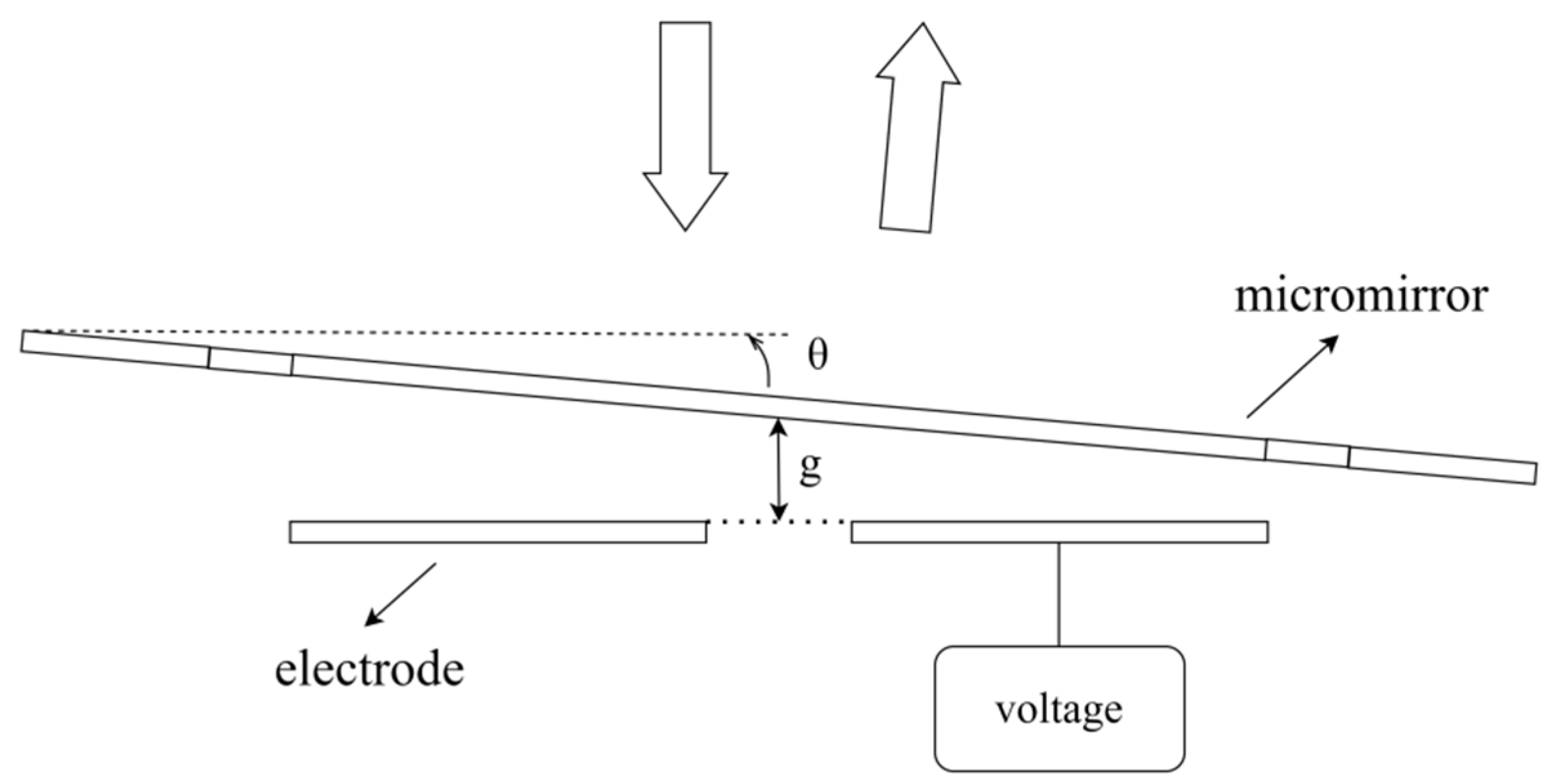
A parallel plate capacitor-based torsional micromirror typically consists of two parts: torsional mirror substrate and counter electrode substrate. As shown in
Figure 1, where g represents the gap between the bottom electrode and the mirror surface, and represents the scanning angle of the micromirror. When a bias voltage is applied to the mirror and counter electrodes, the resulting electrostatic force acts as the driving force to deflect the mirror substrate and change the direction of the light path, thus achieving the modulation of the light.
Parallel plate electrostatic micromirrors often require high driving voltages. To minimize the drive voltage, two main approaches are typically considered. One approach involves minimizing the gap between the micromirror and the driving electrode. However, such a modification would limit the maximum achievable angle of rotation. Another approach is to use compliant torsion bars, which are preferable in reducing the drive voltage. The stiffness of the torsion bar is directly related to the driving voltage. Therefore, optimizing the length and width of the torsion bar can effectively lower the driving voltage. A common method is to utilize serpentine torsional bars design, which increases the length of the bar and subsequently decreases its torsional stiffness. For instance, Sadhukhan [
11] fabricated a comb-drive electrostatic actuator with a square micromirror measuring 5 mm×5 mm, while Xiao et al. from Northwestern Polytechnical University produced an array of electrostatic micromirrors [
12]. In both cases, they utilized serpentine torsional bars to effectively reduce the driving voltage.
In order to achieve larger scanning angles with lower voltage, the serpentine torsion bar is often made thinner and tightly arranged in parallel, which increases the difficulty of fabrication. However, due to limitations in device and fabrication processes, it is not always feasible to continuously optimize the driving voltage by reducing the width of the torsional bars and increasing the length of the torsional bars. As shown in
Figure 2, we have designed two micromirrors to compare their mechanical performance and heat dissipation capabilities with different serpentine torsional bars.
Table 1 presents the main design parameters of the two torsional micromirrors. Micromirror No.1 is characterized by a longer and narrower torsional bar, while micromirror No.2 maintains other parameters unchanged. The torsional stiffness of the torsional bar depends on the material properties and dimensions of the torsional bar and can be expressed as[
13]:
where G is the shear elastic modulus, t is the thickness, w is the width and L is the length of the torsional bar, respectively.
The use of a serpentine torsional bar with narrow dimensions during deep silicon etching may result in the burn of photoresist due to inadequate heat dissipation on the suspended mirror. Upon designing the micromirror and torsional bar dimensions, we employed finite element analysis to predict the heat dissipation capabilities of the two types of micromirrors, thereby allowing us to refine or adjust the design as necessary.
3. Finite element analysis simulation
3.1. Thermodynamic simulation
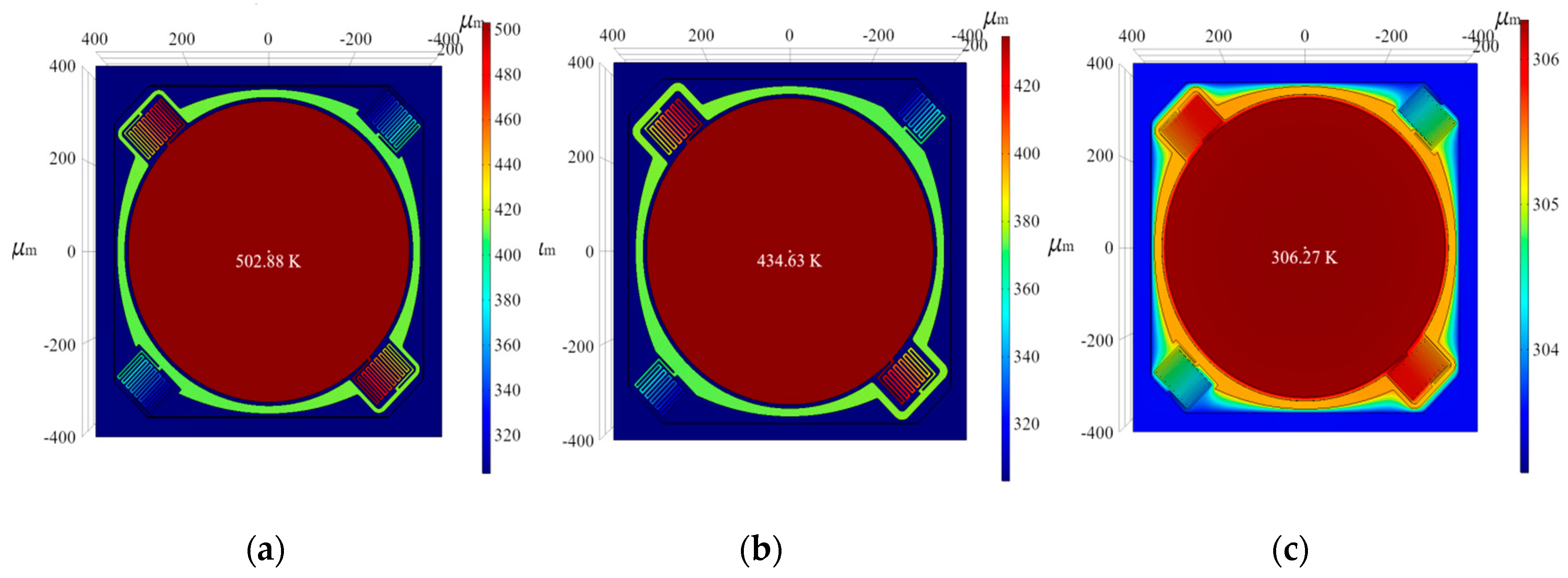
As shown in
Figure 3, we simulated the heat distribution during the etching process of the two types of micromirrors. The ambient temperature was set to 343.15 K, the initial temperature of the chip was 303.15 K, and the glass bottom was kept at a constant temperature of 303.15 K.
Table 2 presents the commonly used etching parameters for deep silicon etching machines, from which the heat flux on the mirror surface during the deep silicon etching process can be estimated to be approximately 2143 W/m
2.
As shown in
Figure 3 (a) and (b), the simulated mirror surface temperature of micromirror No.1 was obtained as 502.88 K, while that of micromirror No.2 was found to be 434.63 K. It can be observed that the heat dissipation capability of the mirror surface significantly decreases when the torsional bar of the micromirror becomes longer and narrower. If the temperature of the mirror surface exceeds the tolerance of the photoresist, it can result in photoresist burn, leading to incomplete etching. To address this issue, we incorporated an oxide layer into the design process, which was added to the back of the micromirror to enhance heat transfer on the mirror during the etching process. As depicted in
Figure 3 (c), the addition of silicon dioxide as a heat dissipation layer results in the heat on the mirror surface being dispersed radially through the silicon dioxide layer, significantly reducing the heat accumulation at the torsional bar. When micromirror No.1 is equipped with a 1000-nm silicon oxide layer as a heat dissipation layer, the surface temperature is only 306.27 K. Furthermore, we conducted simulations using finite element software to investigate the influence of oxide layer thickness on heat dissipation. We applied the same heat flux to the same micromirror with different oxide layer thicknesses of 0.5 μm and 0.2 μm, obtaining simulation results as shown in
Table 3. It can be seen that the addition of the oxide layer significantly reduces the mirror temperature under the same heat flux, while the thickness of the oxide layer has little impact on the result.
3.2. Mechanical performance simulation
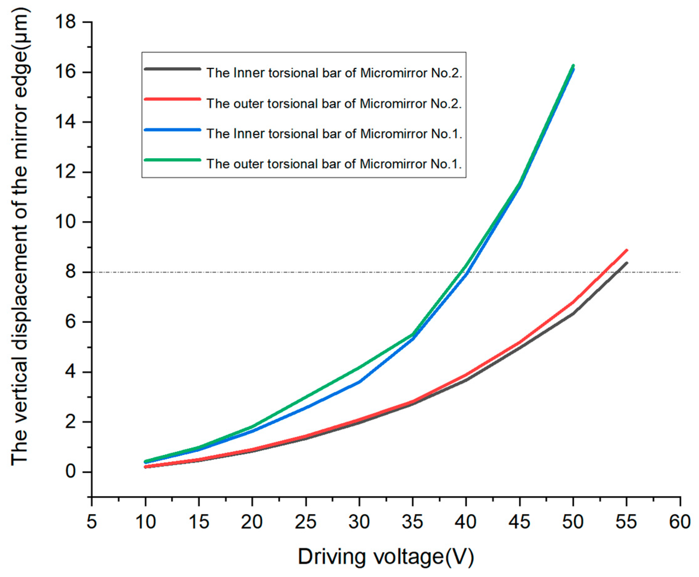
Additionally, we conducted simulation analysis of the mechanical performance of the micro-mirrors using the solid mechanics module and electrostatic module in the finite element software. When an excitation is applied to the bottom electrodes, the mirror surface of the micromirror undergoes motion due to electrostatic attraction. Taking a point at the edge of the micromirror, the mechanical rotation of the micromirror is characterized by its displacement component perpendicular to the bottom electrode. From
Figure 4, the observed results reveal that micromirror No.2 achieves an 8-micrometer displacement with an approximate voltage of 53 V, whereas micromirror No.1 accomplishes the same displacement with only around 40 V. This demonstrates that increasing the length of the torsion axis and reducing its width can indeed decrease the torsional stiffness coefficient of the torsion axis, thereby reducing the driving voltage required. These simulation findings are consistent with the theoretical analysis.
Through finite element simulation analysis, we have observed the feasibility of using silicon dioxide as a heat dissipation layer for deep silicon etching. To validate this approach, we further investigate micromirror No.1 as the research object to study whether the presence or absence of silicon dioxide will have a decisive impact on deep silicon etching for micromirrors with elongated torsional bars.
4. Fabrication
For micromirrors using parallel plate capacitive driving principle, it is necessary to create a certain gap between the micromirror and the driving electrode to allow for the torsional movement of the mirror. Wafer bonding is a widely used method for achieving the gap. Glass, being electrically insulating, allows for natural electrical isolation when fabricating the driving electrodes on it, eliminating the need for additional electrical isolation steps. This simplifies the fabrication process and reduces power consumption during micromirror operation. Additionally, compared to silicon-to-silicon direct bonding, silicon-to-glass anodic bonding offers higher bonding strength and lower bonding temperatures, resulting in a more stable bond interface. In this study, the fabrication process adopts silicon-to-glass anodic bonding to achieve the torsional gap in the micromirror. Due to the ease of controlling silicon etching compared to glass, the top silicon layer of a Silicon-On-Insulator (SOI) substrate is used to create the desired gap and device thickness. This top silicon layer is bonded to a glass substrate with driving electrodes. After removing the bottom silicon layer of the SOI substrate and the buried oxide layer in between, the mirror's reflective coating is applied, followed by etching to release the micromirror structure. This proposed fabrication process is simple, requiring only four lithography steps, eliminating the need for sacrificial and electrical isolation layers. The resulting structure is stable and highly reliable, making it suitable for the production of micromirror arrays and possessing significant practical value.
In this study, we aimed to investigate the effect of a SiO
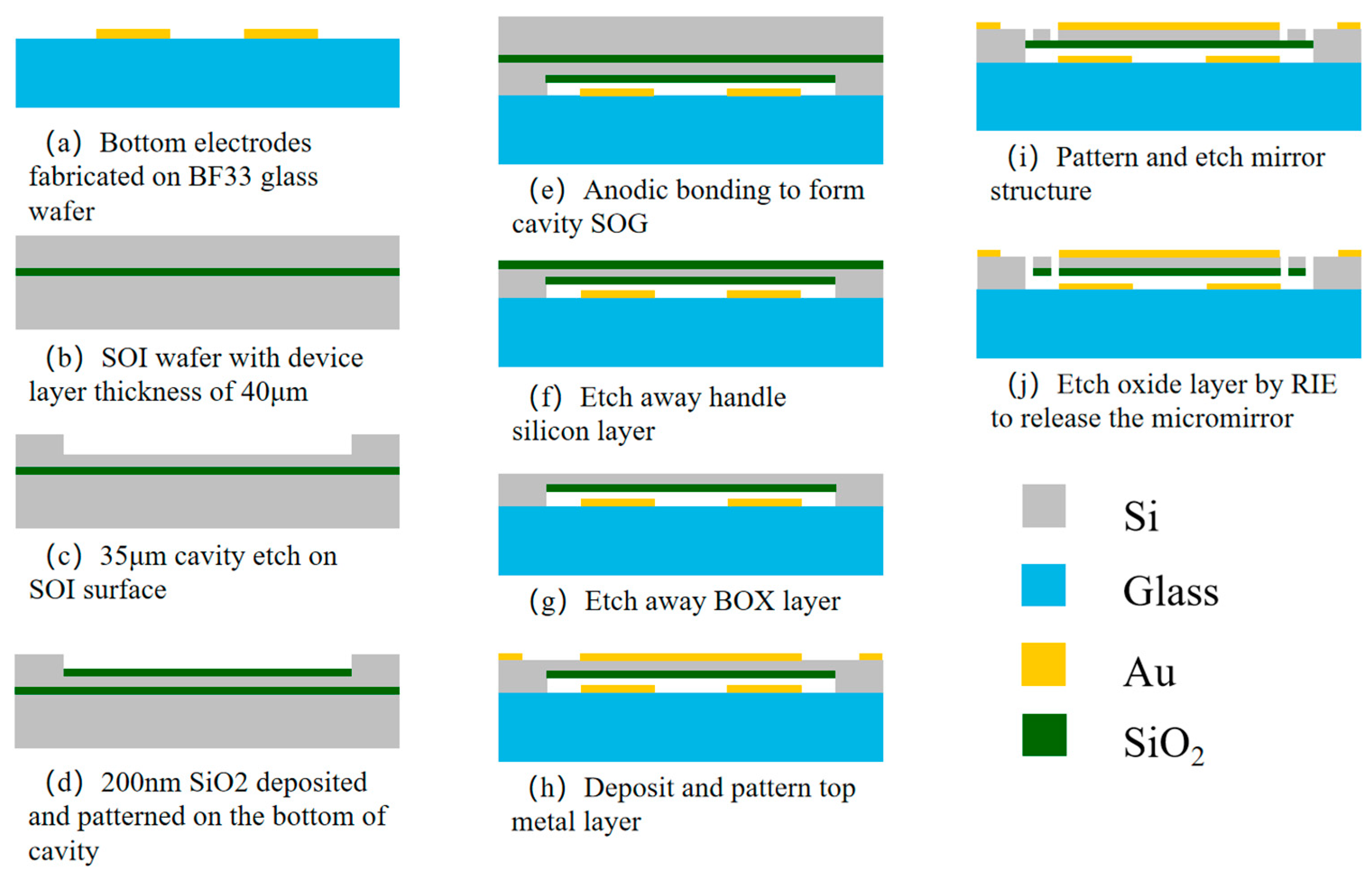
2 heat dissipation layer on the etching of electrostatic torsional micromirrors. We fabricated two types of micromirrors using anode bonding, one with the heat dissipation layer and the other without. For the micromirrors with the heat dissipation layer, the fabrication sequence is shown in
Figure 5. The specific micro mirror fabrication process is as follows:
(a) Bottom Driving Electrodes Fabrication: A 6-inch Borofloat 33 glass wafer, with a thickness of 500 μm, was chosen and meticulously cleaned. Subsequently, a Ti (20 nm)/Au (200 nm) metal layer was deposited on the glass using magnetron sputtering to create the bottom driving electrode.
(b) SOI Wafer Preparation: A 6-inch SOI wafer with a top silicon layer thickness of 40 μm was chosen and cleaned.
(c) DRIE for Cavity Gap Formation: The cavity gap was etched to a depth of 35 μm.
(d) Heat Dissipation Layer Fabrication: A 200-nanometer-thick SiO2 layer was grown in the cavity through plasma-enhanced chemical vapor deposition (PECVD) to function as the heat dissipation layer
(e) Anodic Bonding to Form Cavity SOG: Anodic bonding was employed to tightly integrate the processed SOI wafer and the glass wafer under specific conditions.
(f) Removal of SOI's Handle Silicon Layer: The handle silicon layer of the SOI wafer was thinned to around 100 micrometers and then etched in a 25% Tetramethylammonium hydroxide(TMAH) solution at 85 ℃ until reaching the oxide layer.
(g) Removal of SOI's BOX Layer: The buried oxide (BOX) layer was removed by immersing it in buffered oxide etch(BOE) solution.
(h) Deposit and Pattern Top Metal Layer: A Ti (20 nm)/Au (200 nm) metal layer was sputtered, and then lithography and ion beam etching(IBE) were used to obtain the top electrode and mirror reflective coating.
(i) DRIE for Micro Mirror Formation: The etching continued until reaching the heat dissipation layer.
(j) Micro Mirror Structure Release: The SiO2 heat dissipation layer was removed using reactive ion etching(RIE), and after laser scribing, the micromirror array bare chips were obtained.
In contrast, for the micromirrors without the heat dissipation layer, we omitted the step of growing silicon oxide in the cavity of the SOI device layer. Instead, we directly bonded the SOI with the cavity to the glass with bottom electrode. These fabrication processes allowed us to compare the effects of the SiO2 heat dissipation layer on the etching of the micromirrors.
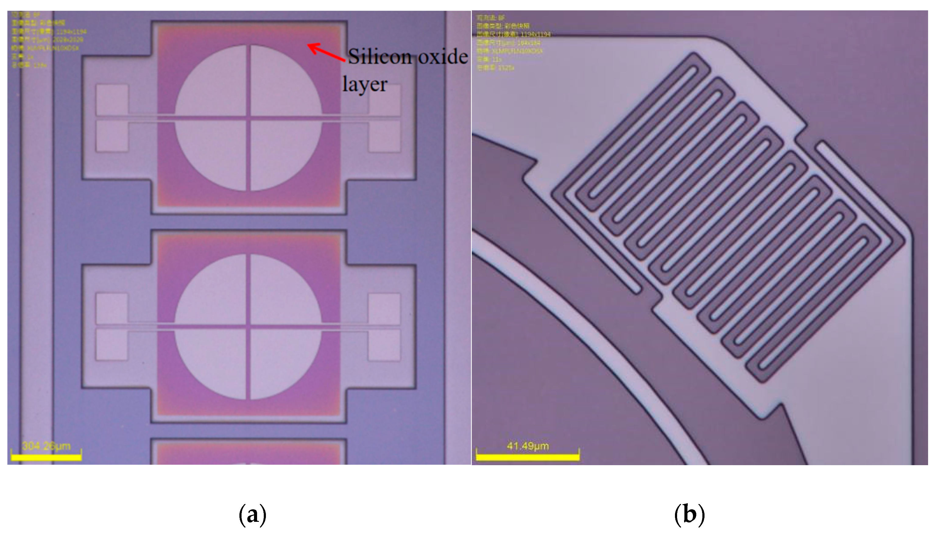
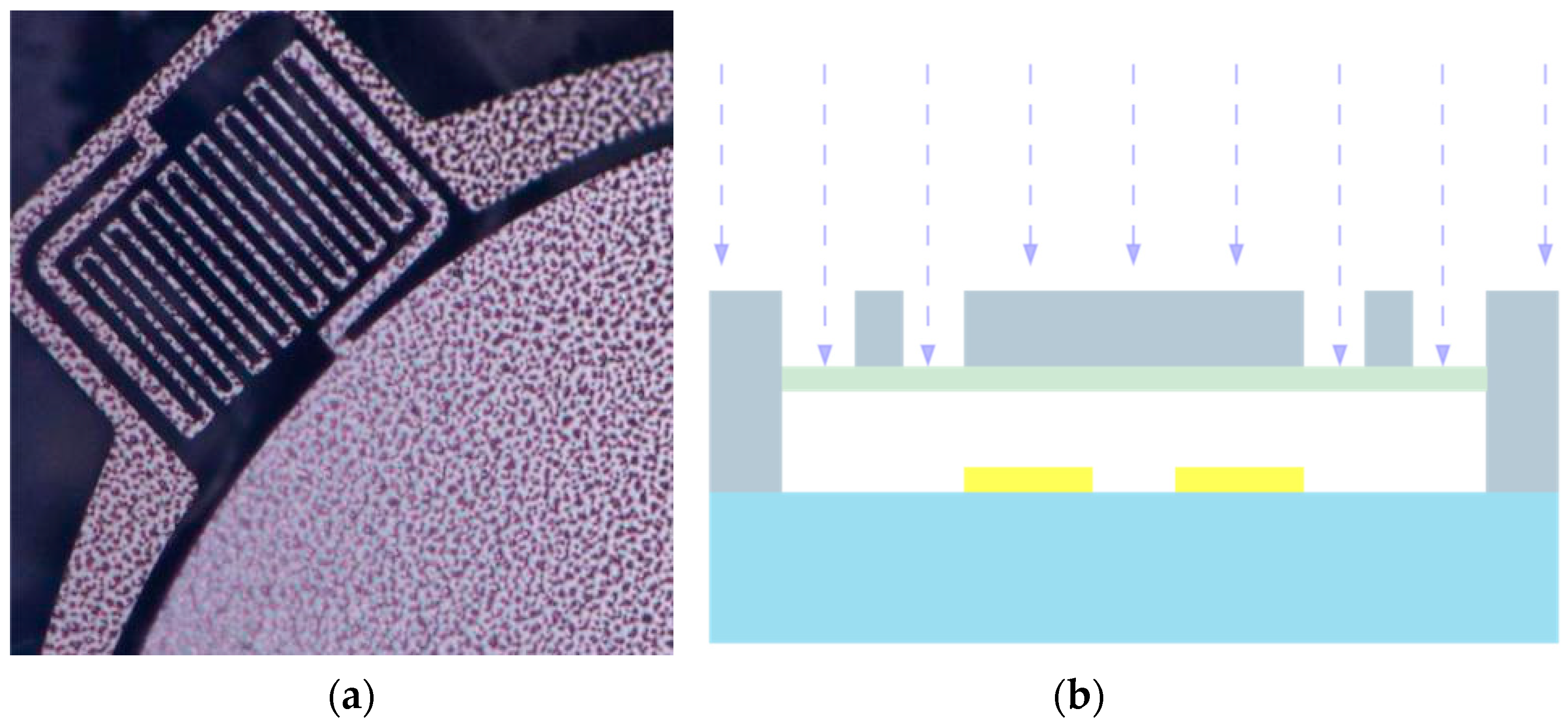
Figure 6(a) shows the results of forming cavity SOG through anode bonding, with arrows indicating the presence of the oxide layer that is deposited at the bottom of the device layer.
Figure 6(b) shows the mask made using AZ5214 photoresist prepared for DRIE as depicted in
Figure 5(i). The photolithography process is observed to be successful, without any issues arising from poor mask fabrication that could affect the deep silicon etching.
5. Experiments and Discussion
Fabricating electrostatic torsional micromirrors is a complex process that requires overcoming several challenges. One of the challenges is the accumulation of heat on the suspended mirror during continuous etching [
14]. This issue can result in photoresist burning and deformation of the polymer in the photoresist, leading to poor etching results and the structural damage. As can be seen from
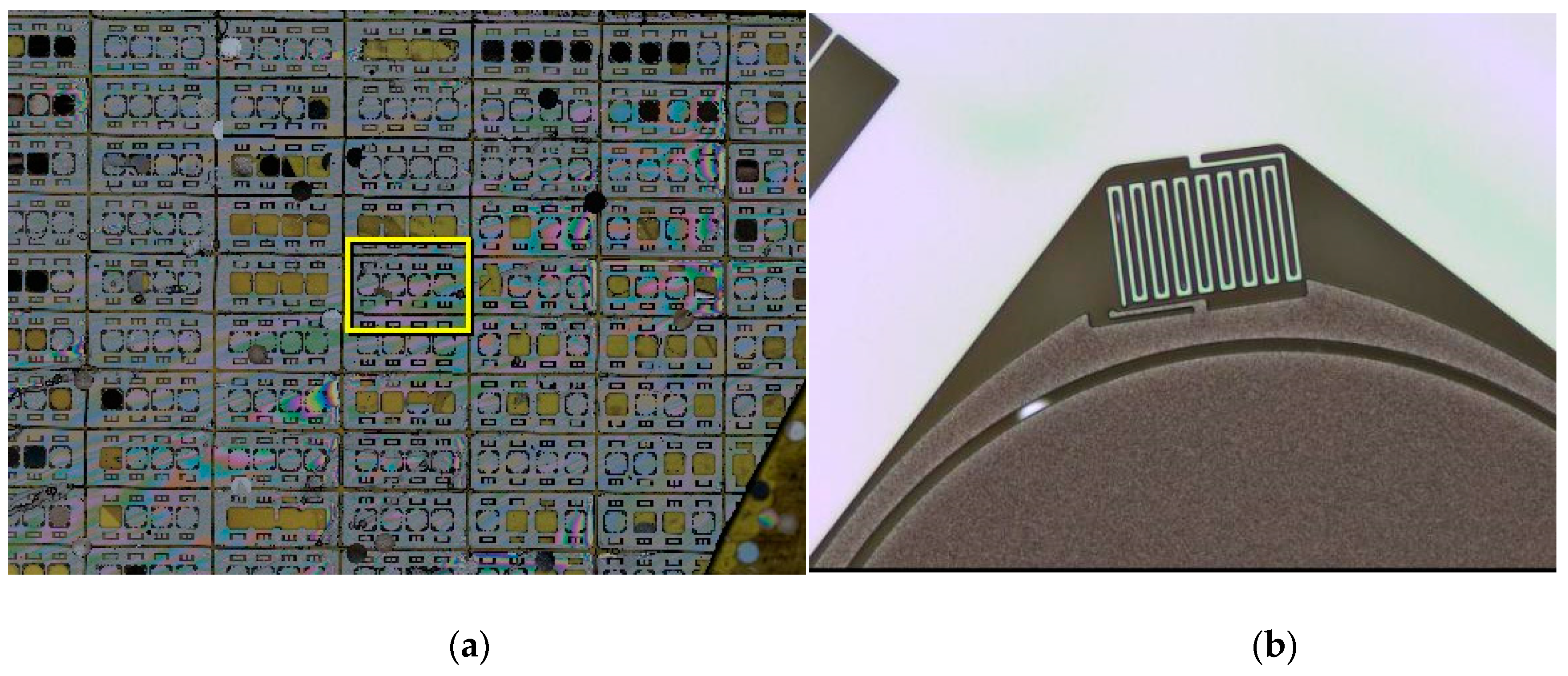
Figure 7(a), for the micromirrors without the heat dissipation layer, as in the previous analysis and simulation, a large proportion of the mirror structures crack, and the photoresist on the mirror surfaces is burned. In
Figure 7(b), it can be observed that the mirror has detached from the outer torsional bar. These observations suggest that the absence of a SiO
2 heat dissipation layer can lead to poor etching results, resulting in the photoresist burning and structrual damage of the mirrors. This can negatively impact the overall performance of the electrostatic torsional micromirrors, and highlights the importance of utilizing a heat dissipation layer in the fabrication process.
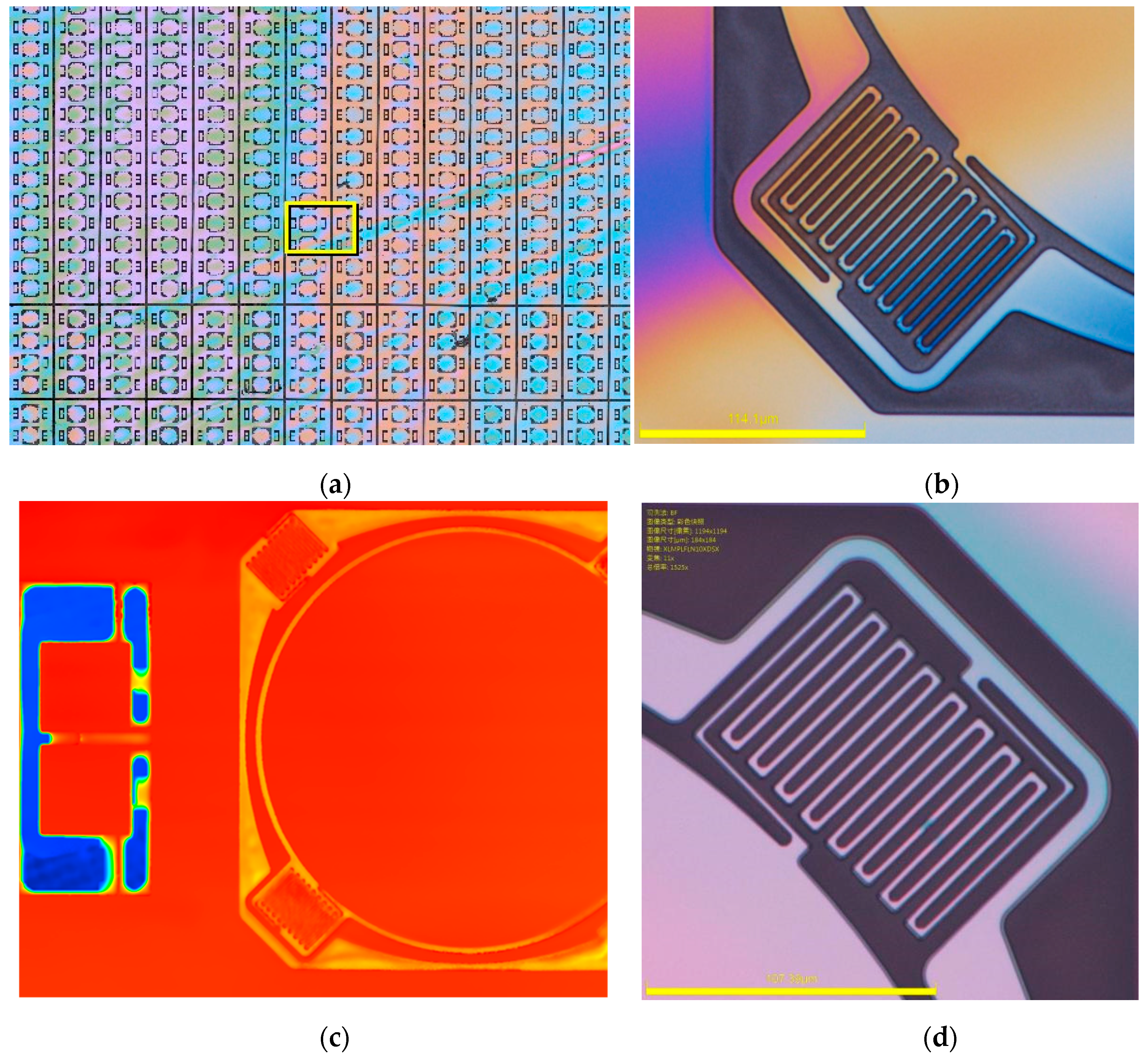
In deep silicon etching, the edges of the wafer typically were etched faster than the central region, necessitating an increase in etching time to ensure complete etching of the micromirrors across the entire wafer. However, for the micromirrors with the heat dissipation layer, as demonstrated in
Figure 8(a), no significant photoresist burning was observed even with over-etching of the micromirrors. As shown in
Figure 8(c), the contour measurement of the micro mirror after deep silicon etching using a profilometer reveals that silicon dioxide does not exhibit any cracking or collapse, indicating its stability and integrity even after deep silicon etching. Furthermore,
Figure 8(b) indicates that the torsional bars did not exhibit any signs of damage, indicating that the addition of silicon oxide has effectively protected the structure.
Figure 8(d) demonstrates that after removing the silicon oxide layer through RIE, the torsional bars remain intact and the micromirrors are successfully released.
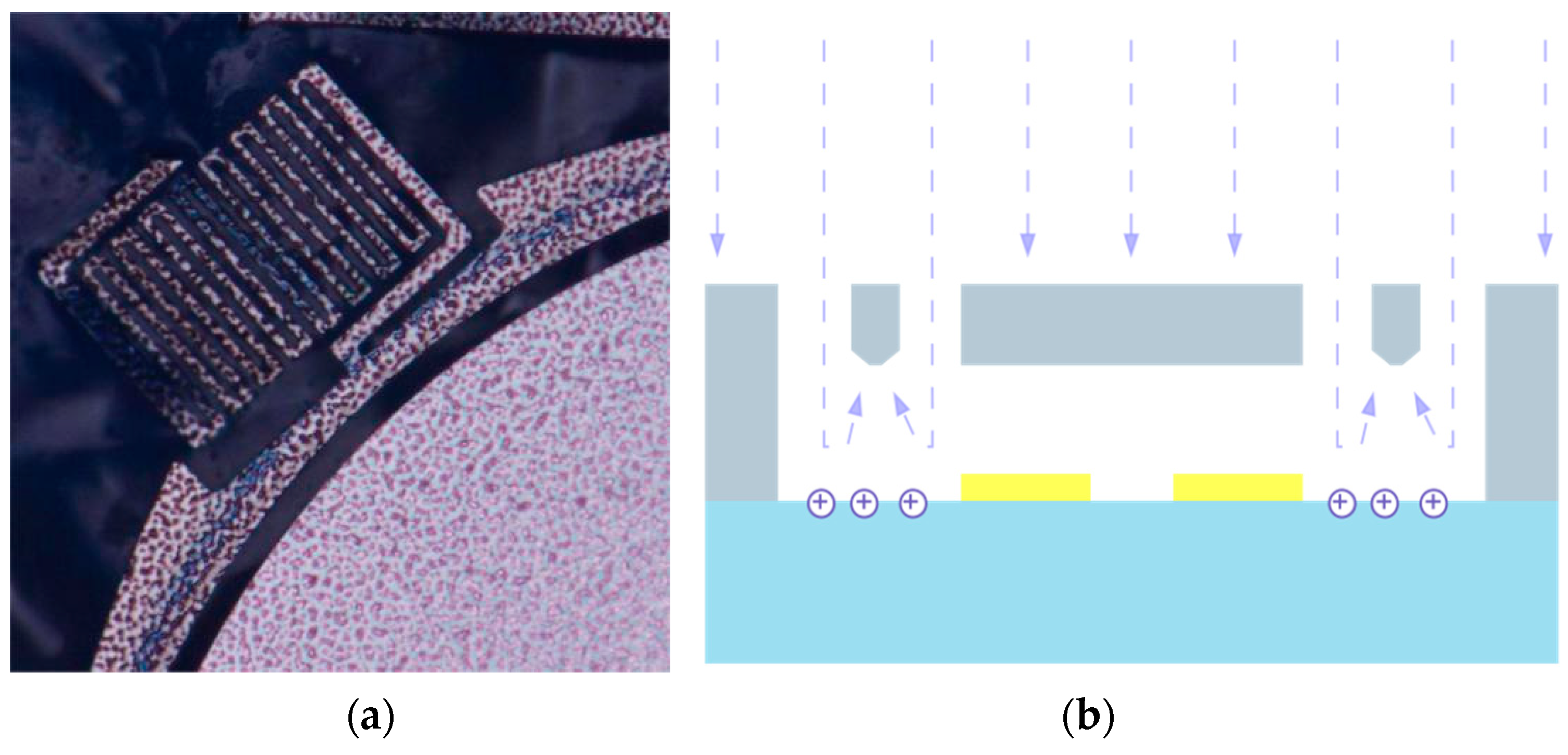
Another challenge is the accumulation of charges on the glass surface due to ion bombardment, as illustrated in
Figure 9(b). This issue can lead to electrostatic deflection of charged ions, resulting in uneven etching or even fracture of the suspended structures [
15]. Traditionally, a solution to the problem of electrostatic deflection has been to lay a metal layer on the glass below the suspended bars [16-20]. However, this method is not always suitable for all anode bonding devices, as the electrical connection between the metal layer and the silicon substrate is difficult to establish, leading to poor bonding quality, particularly for devices such as micromirror array with limited bonding areas.
As depicted in
Figure 9(a), visible etching marks were observed on the silicon backside of the micromirror without the heat dissipation layer, a common phenomenon caused by charging effects during the etching process. In contrast, as illustrated in
Figure 10, the silicon backside in the micromirror with the heat dissipation layer was effectively shielded by the oxide layer, and therefore remained unaffected by the etching ions reflected from the glass substrate. The observed unevenness in the mirror backside was a direct result of the utilization of DRIE to etch cavity to achieve the appropriate thickness during the fabrication process, as illustrated in
Figure 5(c).
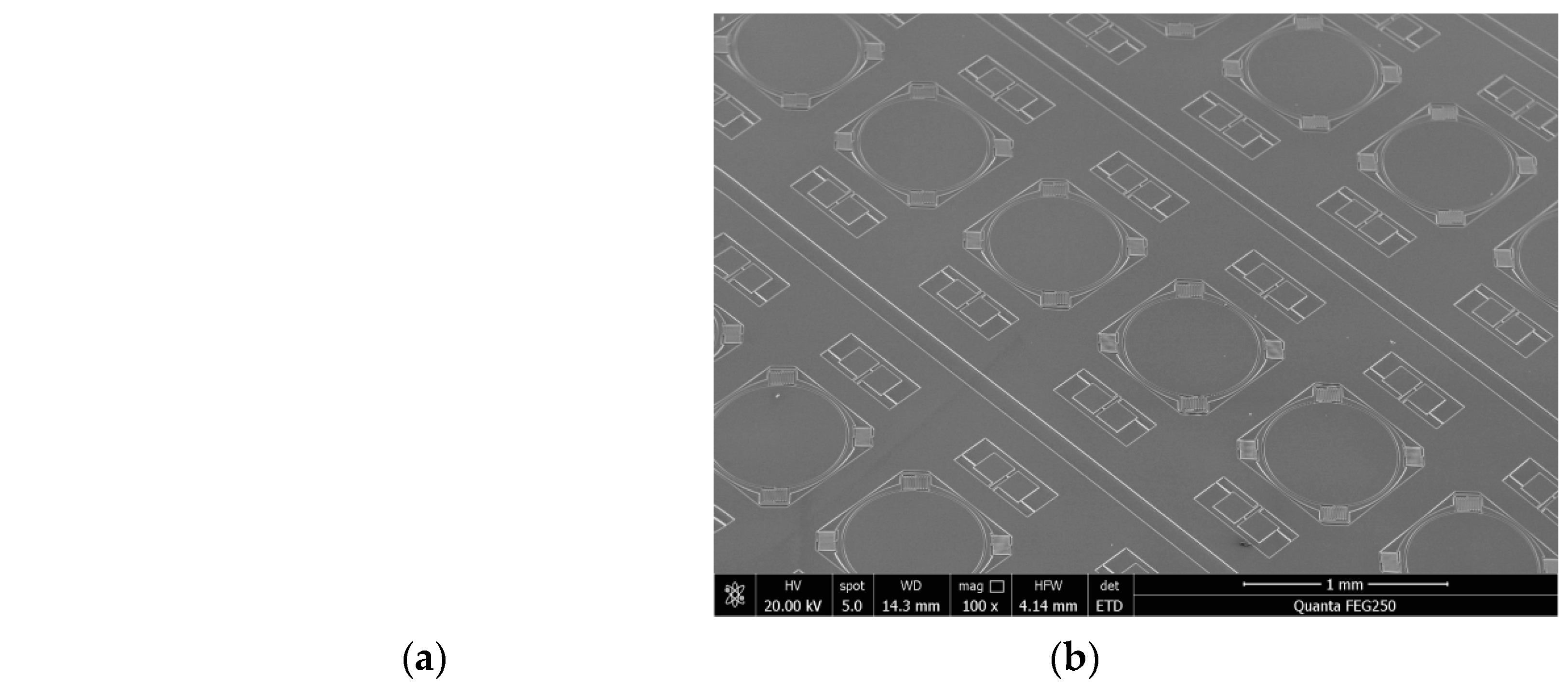
Figure 11(a) depicts the successful removal of the oxide layer on the backside of the experimental group device through RIE. Despite undergoing both over-etching in deep silicon etching and RIE etching, the device remained structurally sound, with the torsional bars made of silicon material remained undamaged. This result demonstrates the efficacy of the RIE method for the release of micromirrors, which is critical for the successful fabrication of micromirror array. Furthermore, as shown in
Figure 11(b), the yield of the devices on the entire wafer was significantly improved, and the fabrication of the micromirror array was achieved.
6. Conclusions
The current study aims to tackle the persistent issue of inadequate heat dissipation and charging effects that frequently afflict anode bonding devices during the DIRE process. To overcome these issues, Our study involves theoretical and simulation analysis of commonly used electrostatic torsional micromirrors with SOG structures. We propose a novel method of growing silicon oxide on the backside of the device layer, and successfully demonstrate the fabrication of micromirror arrays with elongated torsional bars using this approach. Our research has demonstrated that the integration of a silicon oxide heat dissipation layer has a significant mitigating effect on the occurrence of photoresist burning and mirror fracture during the DIRE process. Furthermore, this innovative method holds great potential for enhancing heat dissipation in anode bonding devices, while also effectively preventing etching ions from entering the cavity, thus reducing the risk of device damage.The implications of this method extend beyond the realm of electrostatic torsional mirrors. It offers a promising solution to address heat dissipation issues for other devices with suspended structures that require DIRE. Moreover, it holds great potential in addressing the charging effects commonly seen in the DIRE process.
References
- Algamili, A.S.; Khir, M.H.M.; Dennis, J.O.; Ahmed, A.Y.; Alabsi, S.S.; Hashwan, S.S.B.; Junaid, M.M. A Review of Actuation and Sensing Mechanisms in MEMS-Based Sensor Devices. Nanoscale Res. Lett. 2021, 16, 21. [Google Scholar] [CrossRef] [PubMed]
- Zhu, J.X.; Liu, X.M.; Shi, Q.F.; He, T.Y.Y.; Sun, Z.D.; Guo, X.G.; Liu, W.X.; Bin Sulaiman, O.; Dong, B.W.; Lee, C. Development Trends and Perspectives of Future Sensors and MEMS/NEMS. Micromachines 2020, 11, 30. [Google Scholar] [CrossRef]
- Lee, C.; Lim, Y.; Yang, B.; Kotlanka, R.; Heng, C.; He, J.; Tang, M.; Xie, J.; Feng, H. Theoretical comparison of the energy harvesting capability among various electrostatic mechanisms from structure aspect. Sens. Actuators A 2009, 156, 208–216. [Google Scholar] [CrossRef]
- Koh, K.; Lee, C.; Kobayashi, T. A piezoelectric-driven three-dimensional MEMS VOA using attenuation mechanism with combination of rotational and translation Effects. IEEE/ASME J. Microelectromech. Syst. 2010, 19, 1370–1379. [Google Scholar] [CrossRef]
- Wang, N.; Tsai, J.; Hsiao, F.; Soon, B.; Kwong, D.; Palaniapan, M.; Lee, C. Experimental investigation of a cavity-mode resonator using a micromachined two-dimensional silicon phononic crystal in a square lattice. IEEE Electron Device Lett. 2011, 32, 821–823. [Google Scholar] [CrossRef]
- Wu, D.; Wu, Y.; Chu, J. New progress of anodic bonding technology and its applications in micro-sensor. Sensor technology 2002, 21, 4–7. [Google Scholar]
- Ishihara, K.; Yung, C.F.; Ayon, A.A.; Schmidt, M.A. An inertial sensor technology using DRIE and wafer bonding with interconnecting capability. J. Microelectromech. Syst. 1999, 8, 403–408. [Google Scholar] [CrossRef]
- Cheng, S.W.; Weng, J.C.; Hung, C.H.; Li, C.P.; Meng, C.H.; Liang, K.C.; Fang, W.L.; Ieee. Oxide or Metal Interface Damage Improvement of Deep Silicon Etch Process by Low Power RF of Low Frequency. In 2015 Ieee Sensors, Busan, SOUTH KOREA, Nov 01-04, 2015; Ieee: NEW YORK. 2015; pp. 458–461. [Google Scholar]
- Joudrey, K.; Adams, G.G.; McGruer, N.E. Design, modeling, fabrication and testing of a high aspect ratio electrostatic torsional MEMS micromirror. J. Micromech. Microeng. 2006, 16, 2147–2156. [Google Scholar] [CrossRef]
- Ding, H.T.; Yang, Z.C.; Yan, G.Z.; Ieee. Performance Comparison of Methods to Evading Notching Effect for SOG Structures in DRIE. In 4th IEEE International Conference of Nano/Micro Engineered and Molecular Systems; Shenzhen, PEOPLES R CHINA, Jan 05-08, 2009; Ieee: NEW YORK; 2009; pp. 5–8. [Google Scholar] [CrossRef]
- Sadhukhan, D.; Singh, G.P. Study of electrostatic actuated MEMS biaxial scanning micro-mirror with comb structure. AIP Conf. Proc. (USA) 2020, 2269, 030019–030017. [Google Scholar]
- Xiao, X.C.; Dong, X.; Yu, Y.T. MEMS-based linear micromirror array with a high filling factor for spatial light modulation. Opt. Express 2021, 29, 33785–33794. [Google Scholar] [CrossRef] [PubMed]
- Rezazadeh, G.; Khatami, F.; Tahmasebi, A. Investigation of the torsion and bending effects on static stability of electrostatic torsional micromirrors. Microsystem Technologies-Micro-and Nanosystems-Information Storage and Processing Systems 2007, 13, 715–722. [Google Scholar] [CrossRef]
- Ding, H.-t.; Yang, Z.-c.; Yan, G.-z. A dual-purpose method to enhance heat transfer and prevent notching effect in deep reactive ion etching. Acta Electron. Sin. (China) 2010, 38, 1201–1204. [Google Scholar]
- Fan, J.; Zhu, Y.; Yang, Z.C.; Zhou, J.; Liu, X.S.; Yan, G.Z. An improved method employed in anodic bonded glass-silicon gyroscopes to avoid footing effect in DRIE. In 7th International Conference on Solid-State and Integrated Circuits Technology, Beijing, PEOPLES R CHINA, Oct 18-21, 2004; Ieee: NEW YORK, 2004; pp. 1896–1899. [Google Scholar]
- Chabloz, M.; Jiao, J.; Yoshida, Y.; Matsuura, T.; Tsutsumi, K. A method to evade microloading effect in deep reactive ion etching for anodically bonded glass-silicon structures. Proceedings IEEE Thirteenth Annual International Conference on Micro Electro Mechanical Systems (Cat. No.00CH36308), Conference Paper. 2000; 283–287. [Google Scholar]
- He, K.; Huang, B.; Duan, B.; Song, D.; Guo, Q. Comparison Research on the Protection Methods for MEMS Suspended Structure Deep Reactive Ion Etching. Chin. J. Sens. Actuators (China) 2016, 29, 202–207. [Google Scholar]
- Yoshida, Y.; Kumagai, M.; Tsutsumi, K. Study of silicon backside damage in deep reactive ion etching for bonded silicon-glass structures. Microsyst. Technol. 2003, 9, 167–170. [Google Scholar] [CrossRef]
|
Disclaimer/Publisher’s Note: The statements, opinions and data contained in all publications are solely those of the individual author(s) and contributor(s) and not of MDPI and/or the editor(s). MDPI and/or the editor(s) disclaim responsibility for any injury to people or property resulting from any ideas, methods, instructions or products referred to in the content. |
© 2023 by the authors. Licensee MDPI, Basel, Switzerland. This article is an open access article distributed under the terms and conditions of the Creative Commons Attribution (CC BY) license (https://creativecommons.org/licenses/by/4.0/).
