Preprint
Article

Grafting amino groups onto polyimide films in flexible copper clad laminates using helicon plasma

Altmetrics

Downloads

88

Views

20

Comments

0

A peer-reviewed article of this preprint also exists.

Submitted:

30 July 2023

Posted:

01 August 2023

You are already at the latest version

Alerts
Abstract
Polyimide (PI) films are widely used in electronic devices owing to their excellent mechanical and electrical properties and high thermal and chemical stabilities. In particular, PI films play an important role in flexible printed circuit boards (FPCBs). However, one challenge currently faced with their use is that the adhesives used in FPCBs cause a high dielectric loss in high-frequency applications. Therefore, it is envisioned that PI films with a low dielectric loss and Cu films can be used to prepare two-layer flexible copper clad laminates (FCCLs) without any adhesive. However, the preparation of ultra-thin FCCLs with no adhesives is difficult owing to the low peel strength between the PI films and Cu films. To address this technical challenge, an FCCL with no adhesive was prepared by high-power helicon wave plasma (HWP) treatment. The surface roughness of the PI film and the peel strength between the PI film and Cu film were measured. The experimental results showed that the surface roughness of the PI film increased by 40-65% and the PI film demonstrated improved adhesion (the peel strength was >8.0 N/cm) with the Cu film following plasma treatment and Cu plating.
Keywords: 
Subject: Chemistry and Materials Science  -   Materials Science and Technology

1. Introduction

In recent years, with the development of small and light electronic devices, the demand for flexible electronic components has increased. In particular, flexible printed circuit boards (FPCBs) have garnered great interest. An FPCB with excellent material performance needs to be prepared with high-quality, flexible copper clad laminate (FCCLs). Owing to their excellent mechanical and electrical properties [1] as well as high chemical and thermal stabilities [2], polyimide (PI) films have become an important material for preparing FCCLs [3,4,5,6,7]. However, owing to their low roughness and smooth surface, PI films have a low adhesion strength with Cu films [8], necessitating the use of adhesives. Further, many adhesives exhibit high dielectric loss during high-frequency applications. Therefore, to manufacture adhesive-free FPCBs, PI films need to be modified to increase their adhesion strength with Cu films prior to FCCL preparation [9,10,11].
Conventional PI film surface modification methods include acid or alkali treatment [12,13,14], ion beam etching [15], and grafting functional groups onto a surface by plasma treatment [16,17,18,19]. Acid or alkali treatment is a surface modification method used to increase the surface energy and adhesive properties of PI films by hydrolyzing the surface imide group into polyamide acid and its associated metal salt. Since PI does not exhibit a high alkaline resistance, alkaline hydrolysis can easily and efficiently change the structure and morphology of the PI film surface. Likewise, ion beam etching improves the mechanical and adhesive properties of PI films by controlling molecular aggregation through physical methods. The main parameters that control the effectiveness of ion beam etching are the energy, ion current density, and etching time. Finally, grafting functional groups onto a surface by plasma treatment is a method that has become increasingly popular in recent years. Particularly, non-thermal plasma treatment is often used for the surface modification of polymeric materials. Plasma is considered a fully or partially ionized gas state of a substance [20], which may contain atoms, molecules, metastable ions, and excited ions. The contents of electrons, anions and cations in the plasma are nearly the same. Plasma has a high energy density and easily undergoes physical and chemical reactions with other substances. Grafting amino groups onto PI films by plasma can quickly change the surface composition of the PI films without affecting their bulk-phase composition. This method can be optimized by identifying suitable processing parameters, thereby creating the ideal working conditions for subsequent treatment following grafting of the amino groups.
Herein, amino groups were grafted onto a PI film using helicon wave plasma (HWP) for the first time. A HWP source is a low-temperature plasma source which has a high plasma density, high ionization efficiency [21], high and uniform electron density, low confining magnetic field, strong controllability [22], and a relatively simple structure. The HWP source can heat a large area of electrons when the helicon wave propagates in the plasma and can discharge at an ultra-low pressure. Helical antennas play an important role in providing the radio frequency power needed for ionizing and heating plasma in the HWP discharge. Based on the results of numerical simulations and experimental research on plasma excited by a helicon wave [23,24,25], a right helical antenna of half wavelength was adopted. In this work, an ultra-high radio frequency power of up to 10 kW was used, leading to an increase in the electron density. The surface roughness and peel strength of the PI film notably increased after the PI film surface was grafted with amino groups by the high-power HWP. The surface roughness of the PI film increased by 40-65% following the plasma treatment, and the PI film demonstrated improved adhesion strength (the peel strength was >8.0 N/cm) with the Cu film after plasma treatment and Cu plating.

2. Experimental Section

2.1. Material Preparation

The PI films (HN type, 25 μm thick, Du Pont) were purchased from a local vendor and were cut into 50 mm × 50 mm pieces, which served as the substrate for surface metallization. After rinsing with deionized water for several times, the PI films were degreased in an ultrasonic bath containing ethanol solution for 30 min, then dried in an oven at 60 °C for 30 min. The as-cleaned PI films were placed in the chamber of a plasma system subjected to a CH4 (99.999%) and NH3 (99.999%) flow of 200 standard cubic centimeter per min (sccm). The working pressure of the plasma treatment was maintained at 0.5 Pa. The radio frequency power with a frequency of 13.56 MHz was set to 4 kW to generate the NH3/CH4 plasma used to bombard the PI surface for several minutes. The PI substrates had a pulsed bias voltage (Vs) within a range of –400-0 V with a frequency of 10 kHz, duty ratio of 20%, and sample temperature of 30 °C, which was measured using a thermocouple in real time. After the plasma process, the samples were cooled to approximately 25 °C under N2 flow. Subsequently, the specimens were sectioned with a width of 1 mm, which were used to probe the surface properties.
Cu films were prepared using self-designed ultra-high-vacuum multi-functional sputtering equipment manufactured by SKY Technology Development Corporation Limited, Chinese Academy of Sciences. The system was pumped, achieving a base pressure of 1×10⁻⁵ Pa before Cu plating. The Cu target (3 inch) was purchased from GRINM Group Corporation Limited. In the Cu plating process, the radio frequency sputtering power ranged from 50 to 120 W, and 99.9999% pure Ar was selected as the working gas. There was no additional heating during Cu plating.
Optical emission spectroscopy (OES) profiles were collected using a grating spectrometer (Princeton Instruments, HRS-750S) and an intensified charge-coupled device (ICCD) camera (Princeton Instruments, PM4-1024i), in combination with a 74-UV silica-collimating lens. The spectra were measured for wavelengths between 200 and 800 nm in increments of 0.03 nm.

2.2. Morphological and Structural Characterization

Field-emission scanning electron microscopy (FE-SEM, SU8010, Hitachi) was employed to observe the morphology and thickness of the coating. X-ray photoelectron spectroscopy (XPS) was used to analyze the elemental composition and chemical bonding of the substrate. A ESCALAB 250XI spectrometer was used in combination with in situ Ar+ ion etching and equipped with a monochromatic Al Kα (hυ = 1,486.6 eV) X-ray source. The base pressure during spectral acquisition was at least 6.6×10⁻¹⁰ mbar. The analyzed sample area was 650 μm. The electron emission angle was set to 58°. The sample sputter-etched period was 10 min, Ar+ energy was 1000 eV, and incidence angle was set to 40° from the vertical. The charge neutralized is used during the XPS experiment. The charge-referencing method used was the work function method. X-ray diffraction (XRD) analysis was performed using an X-ray diffractometer (Bruker D8 Advance, Germany) with a Cu Kα line at 0.15418 nm as a source, in the range of 10°-80° at a scanning rate of 5°/min.

2.3. Mechanical Property Characterization

The roughness was calculated from the roughness profile determined by atomic force microscopy (AFM). Peeling tests were performed to measure the force required to peel off the film per unit width, and the strength was reported in N/cm. The peeling test protocol was followed as described in the literature [26]. The peeling test between the Cu films and PI films was performed six times and the average was reported as the peeling strength.

3. Results and Discussion

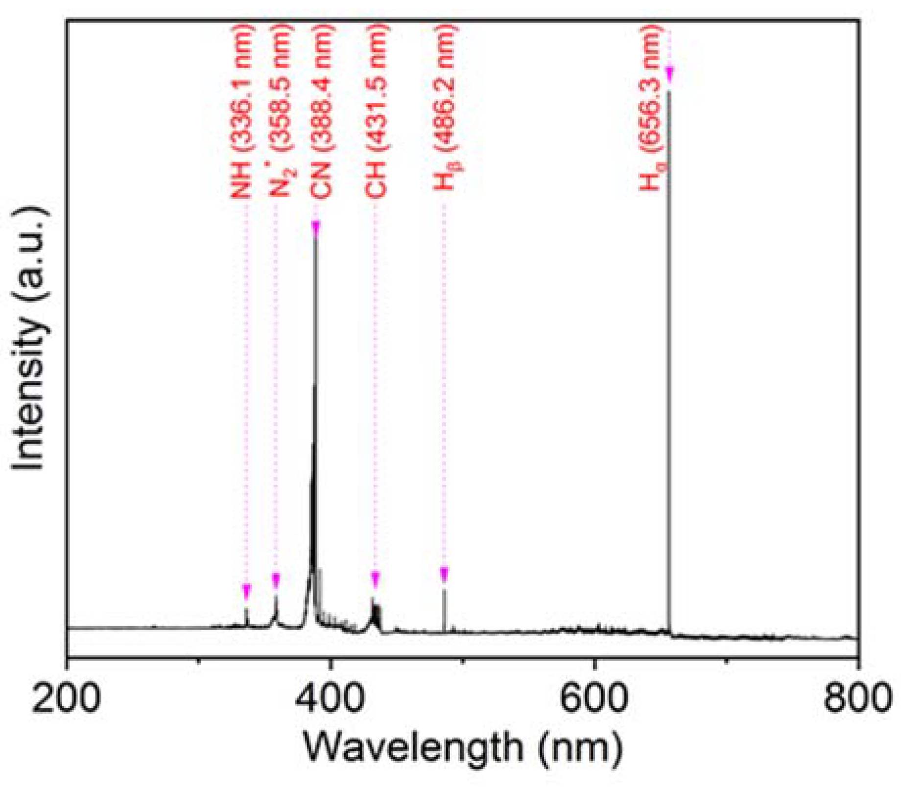
HWP was used to graft amino groups onto the surface of the PI films. The HWP device consists of a plasma source and a material processing chamber. CH4/NH3 was decomposed into reactive radicals in the chamber (Figure 1). During the HWP discharge, OES was used to study the correlation between the grafted amino groups and various other active species. Since the applied Vs has no effect on OES, the typical emission spectrum during HWP discharge at a –Vs of 100 V is displayed in Figure 2 for the spectral range of 200-800 nm. Intense emission peaks of reactive species are observed in the plasma discharge. Specifically, emission peaks of NH (336.1 nm), N2* (358.5 nm), CN (388.4 nm), CH (431.5 nm), Hβ (486.2 nm), and Hα (656.3 nm) are observed. The N2* molecular spectra likely arise from surface air discharge between the outer surface of the reactor and inner surface of the grounding electrode. According to the OES results in the literature [27], a possible fragmentation pathway is as follows: CH4 + NH3 + e → NH, CN, CH, H. This pathway indicates that a higher ne can enhance or promote the dissociation of the precursor. NH and CN transitions were observed in the OES profiles, arising from the decomposition of CH4/NH3 during the HWP discharge, which can be considered as a reaction precursor for the grafting of amino groups. Many energetic H atoms are generated from CH4/NH3 by the HWP discharge, and these H atoms have the ability to eliminate certain unstable phases.
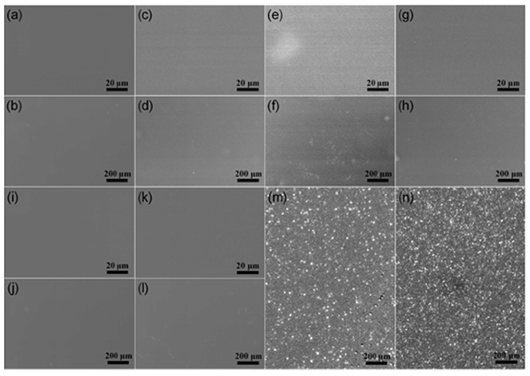
The morphology of the PI films was analyzed using FE-SEM after the amino groups were grafted onto the PI films by high-power HWP. As illustrated in Figure 3a–l, the surface morphology of the PI films changes following plasma treatment. Notably, the surface morphology changes are most pronounced at the –Vs of 100 V, where the roughness of almost the entire surface increases. This result indicates that the effect of plasma treatment is optimal at a –Vs of 100 V. Next, the morphologies of the plasma-treated PI film at –Vs = 100 V and the non-treated PI film were compared following Cu plating. As shown in Figure 3m–n, the Cu clusters on the surface of the PI film are not compact after Cu plating on the PI film without plasma treatment and no films are formed, indicating that it is difficult to plate Cu on the PI film without plasma treatment. Further, the Cu atoms on the surface of the PI film form compact clusters after Cu plating on the PI film with plasma treatment at a –Vs of 100 V and a compact film was formed, indicating that the effect of Cu plating on the PI film with plasma treatment at a –Vs of 100 V is very good. Therefore, it can be concluded that plasma treatment can promote Cu plating on PI films. However, the mechanism behind why plasma treatment enhances the Cu plating ability is still unknown and necessitates further investigation and discussion.
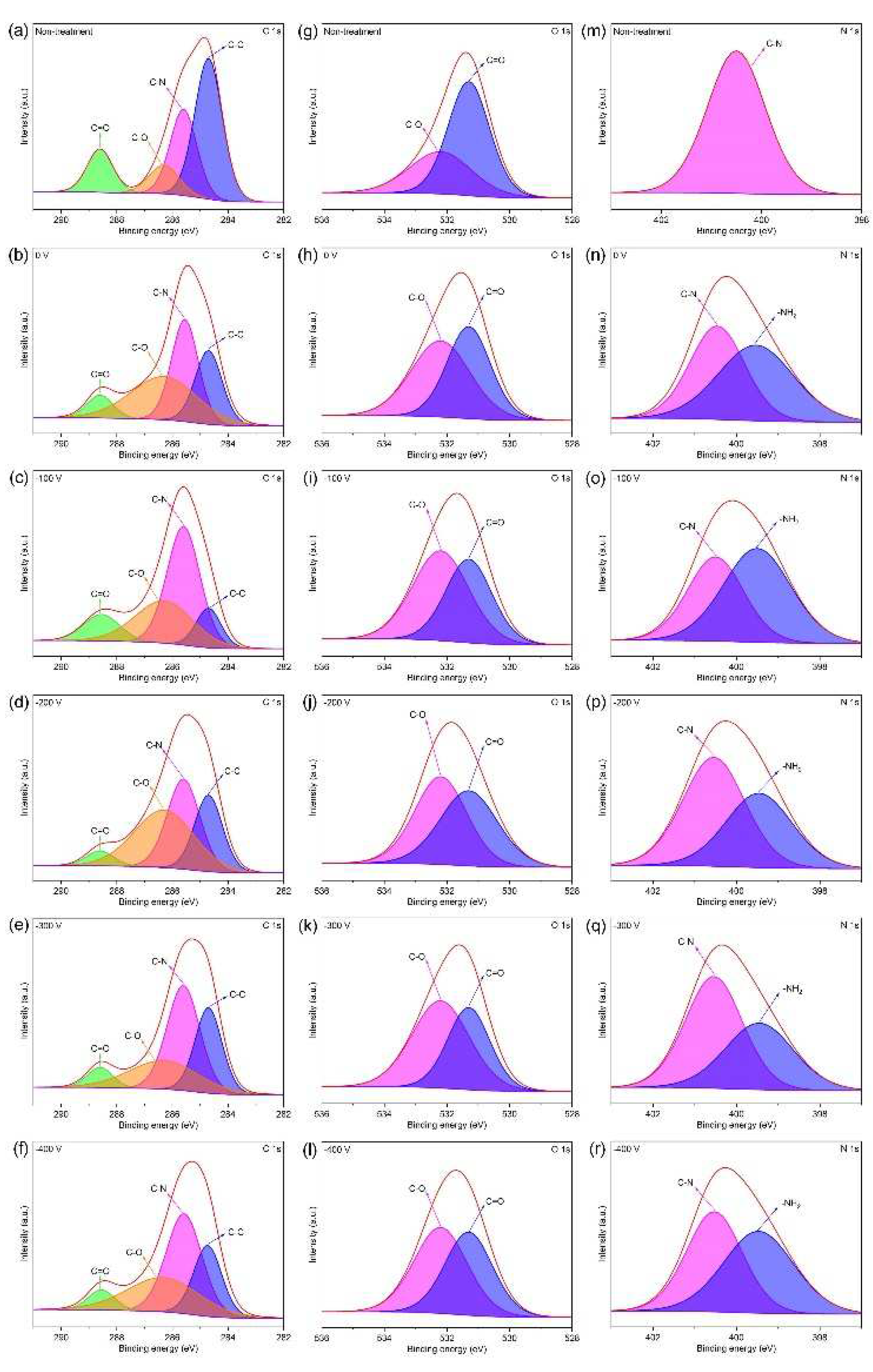
To investigate whether the amino groups were successfully grafted onto the PI film surface, the chemical bonds of the PI films following amino group grafting were analyzed by measuring the XPS profiles of the plasma-treated PI film. As shown in Figure 4a–f, the peaks at approximately 288.6, 286.3, 285.6, and 284.7 eV are the characteristic peaks of the C=O, C−O, C−N, and C−C bonds [28], respectively. The intensity of the characteristic peak for the C−N bond is the highest at the –Vs of 100 V. As shown in Figure 4g–l, the peaks at approximately 532.2 and 531.3 eV are the characteristic peaks of the C−O and C=O bonds [29], respectively. In Figure 4m–r, the spectra of the plasma-treated PI films exhibit the characteristic peaks of the −NH2 [30] and C−N bonds [31], where the binding energies of the N 1s electrons are approximately 399.5 and 400.5 eV, respectively. However, the spectrum of the untreated PI film only contains the characteristic peak of the C−N bond, where the binding energy of the N 1s electrons is approximately 400.5 eV. The characteristic peak intensity of the −NH2 group is the highest at a –Vs of 100 V. The above results indicate that the amino groups are successfully grafted onto the surface of the plasma-treated PI films, and that the degree of amino group grafting is optimized at a –Vs of 100 V.
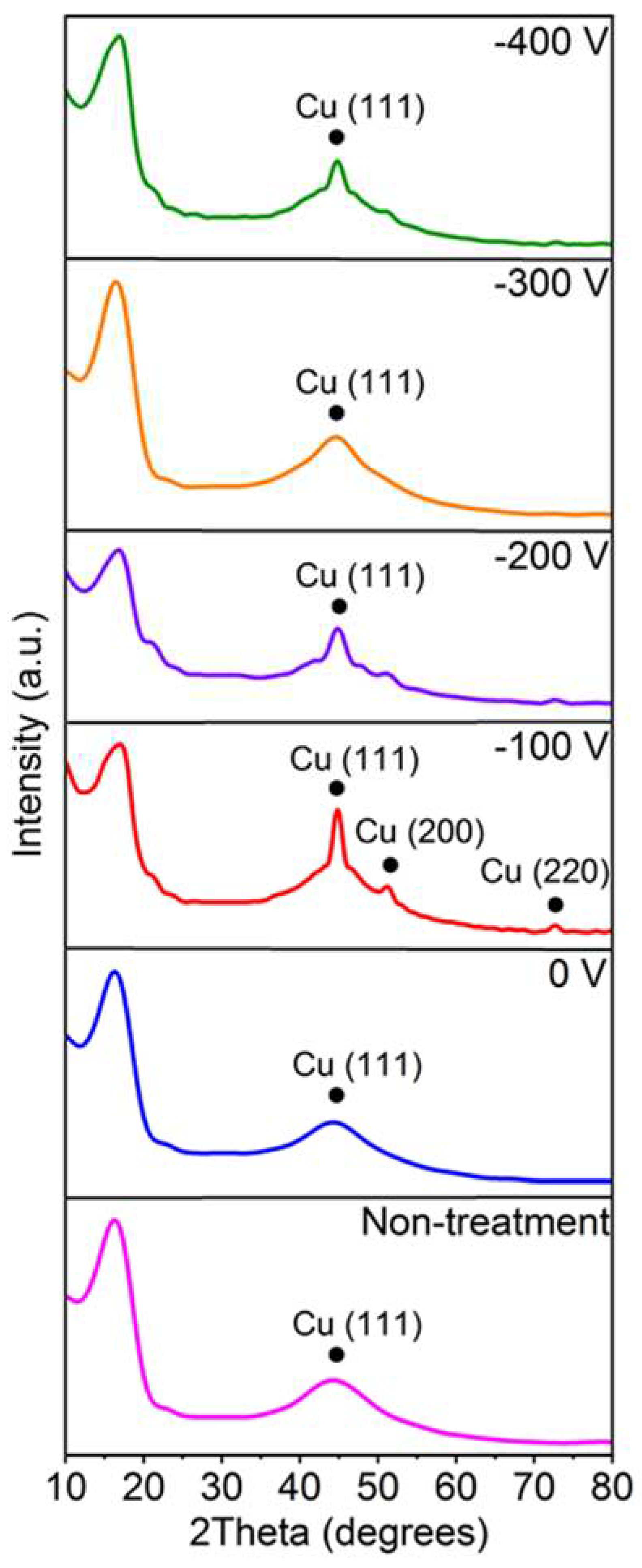
To further characterize the structure of the PI films after Cu plating, the XRD patterns of the treated and non-treated PI films post Cu plating were acquired, and the results are shown in Figure 5. The peak at approximately 16.5° is the characteristic peak of PI [32], and the peaks at approximately 44°, 51°, and 73° are the characteristic peaks of the Cu (111), Cu (200), and Cu (220) crystal planes [33], respectively. As shown in Figure 5, the characteristic peak intensity of Cu is very low after Cu plating on the non-treated PI film, indicating that it is difficult to plate Cu on the non-treated PI film. Among all the plasma-treated PI films at various Vs values, the characteristic peak intensity of Cu is the highest after Cu plating on the PI film with plasma treatment at –Vs = 100 V, indicating that this plasma-treated PI film closely bonds with the Cu film, since the amino group grafting is optimal at these parameters.
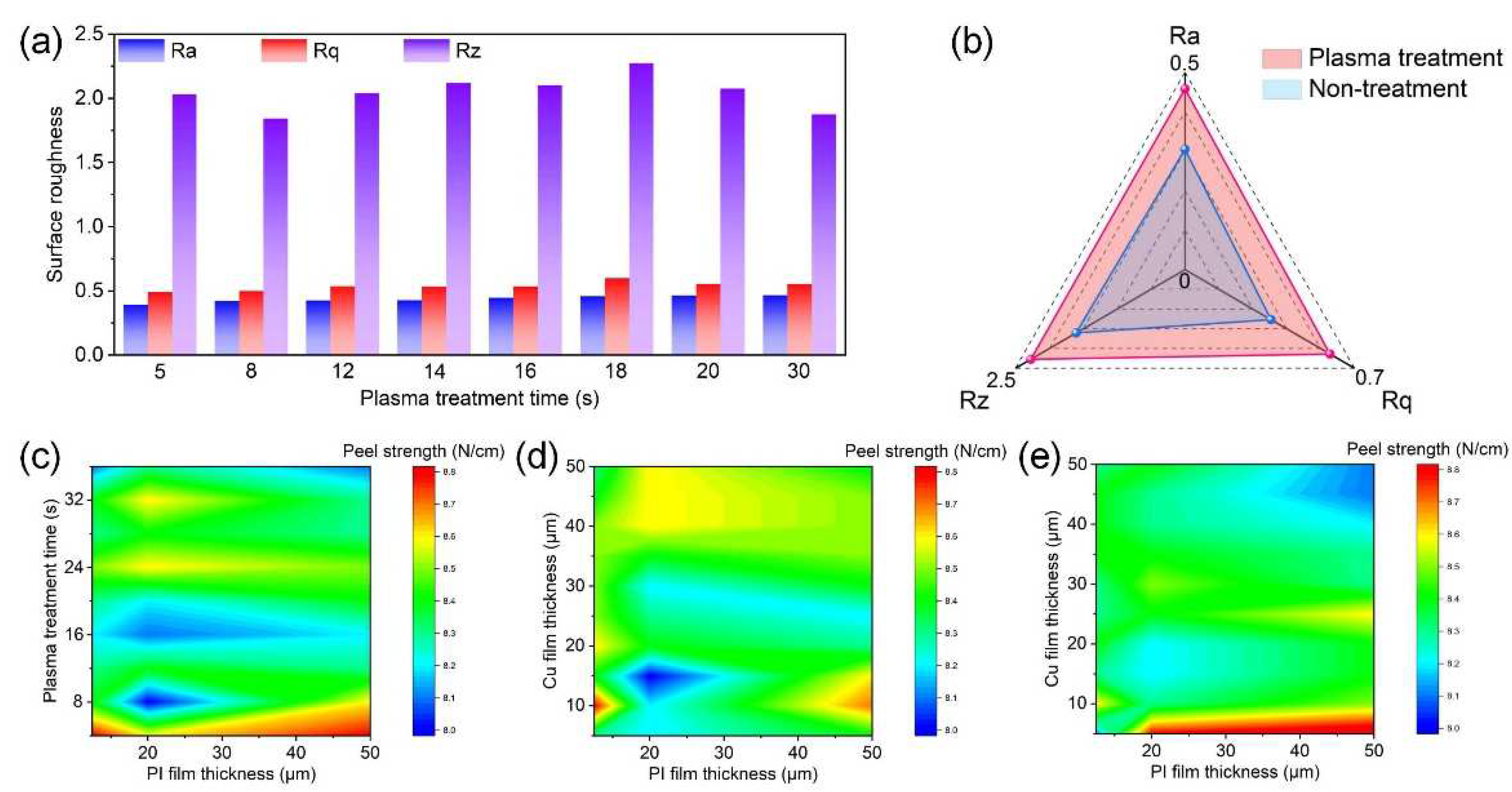
To investigate whether the plasma-treated PI films could improve Cu film adhesion, the surface roughness of the PI films was measured. The surface roughness can reflect the degree of adhesion when Cu films are attached to PI films caused by uneven surface of PI films. PI films with rougher surfaces have larger surface areas, and therefore, exhibit stronger adhesion. Figure 6a displays the surface roughness of the plasma-treated PI films at various times. As shown in Figure 6b, when compared to the untreated PI film, the surface roughness of the PI film increases by 40-65% following plasma treatment. The increase in the surface roughness of the PI film is very beneficial for increasing the adhesion after sputtering/electroless Cu plating [34].
To further investigate whether the PI films subjected to plasma treatment could closely bond with the Cu films, the peel strength between the PI films and Cu films was measured. For a pure elastic case, the peeling force F (N/cm) corresponds to the energy required to separate the Cu/PI interface [26]. The peel strength between the PI films and Cu films also reflects the degree of adhesion between the PI films with Cu films; a higher peeling strength indicates closer bonding. As shown in Figure 6c, the PI film has good adhesion (the peel strength is >8.0 N/cm) with the Cu film following plasma treatment and Cu plating, and the thickness of the PI films does not affect its adhesion abilities. When the plasma treatment time is longer than 8 s, the effectiveness of the treatment is still satisfactory, but subsequently starts to decline. Therefore, the optimal plasma treatment time is between 5 and 8 s. Figure 6d shows the peel strength between the Cu films and PI films, both with various thicknesses, following plasma treatment for 5 s and sputtering Cu plating. The results demonstrate that sputtering Cu plating is suitable for preparing FCCLs with thicker Cu films. Figure 6e depicts the peel strength between the Cu films and PI films, both with various thicknesses, following plasma treatment for 5 s and electroless Cu plating. The results show that the quality of FCCL prepared by electroless Cu plating is comparable to that of the FCCLs prepared by sputtering, but electroless Cu plating is more suitable for preparing FCCLs with thinner Cu films.

4. Conclusions

A high-power HWP device for surface treatment was designed and fabricated, and amino groups were grafted onto a PI film surface using this device. The FE-SEM and XPS results revealed that the amino groups were successfully grafted onto the PI film. Amino grafting was optimal at a –Vs of 100 V. Additionally, the XRD results showed that the PI film subjected to amination treatment adhered well to the Cu film at a –Vs of 100 V. In addition, the surface roughness of the PI film and its peel strength with Cu film following the grafting of the amino groups were measured. The experimental results showed that the surface roughness of the PI film increased by 40-65% following plasma treatment and that the PI film adhered well (the peel strength was >8.0 N/cm) with the Cu film after plasma treatment and Cu plating. In other words, the surface roughness of the PI film subjected to plasma treatment noticeably increased, which was very beneficial for improving its adhesion after sputtering/electroless Cu plating. These results demonstrate that it is possible to prepare FCCLs without the use of adhesives, including ultra-thin FCCLs with a high peel strength. Moreover, the preparation method outlined in this paper is relatively simple, which can reduce environmental waste, reduce the amount of human resources needed, and reduce manufacturing costs.

Author Contributions

Methodology, C.J.; Validation, Y.Z.; Formal analysis, Z.Q.; Investigation, C.J., Z.Q. and J.W.; Resources, J.W.; Data curation, C.W.; Writing – original draft, C.J., C.W. and Y.Z.; Writing – re-view & editing, S.S. and L.H.; Project administration, P.E.; Funding acquisition, P.E. All authors have read and agreed to the published version of the manuscript.

Funding

This work was supported by CGN-HIT Advanced Nuclear and New Energy Research Institute (Grant No. CGN-HIT202203), the Fundamental Research Funds for the Central Universities, a project from the National Development and Reform Commission (NDRC), SESRI (Space Environment Simulation Research Infrastructure) being developed in the city of Harbin, China.

Data Availability Statement

Data will be made available on request.

Conflicts of Interest

The authors declare no conflict of interest.

References

  1. Cen-Puc, M.; Schander, A.; Gleason, M.G.V.; Lang, W. An assessment of surface treatments for adhesion of polyimide thin films. Polymers 2021, 13, 1955. [Google Scholar] [CrossRef]
  2. Liu, T.J.; Chen, C.H.; Wu, P.Y.; Lin, C.H.; Chen, C.M. Efficient and adhesiveless metallization of flexible polyimide by functional grafting of carboxylic acid groups. Langmuir 2019, 35, 7212–7221. [Google Scholar] [CrossRef]
  3. Yang, S.; Wu, D.; Qi, S.; Cui, G.; Jin, R.; Wu, Z. Fabrication of highly reflective and conductive double-surface-silvered layers embedded on polymeric films through all-wet process at room temperature. J. Phys. Chem. B 2009, 113, 9694–9701. [Google Scholar] [CrossRef]
  4. Ho, S.M.; Wang, T.H.; Chen, H.L.; Chen, K.M.; Lian, S.M.; Hung, A. Metallization of polyimide film by wet process. J. Appl. Polym. Sci. 1994, 51, 1373–1380. [Google Scholar] [CrossRef]
  5. Ng, J.H.G.; Desmulliez, M.P.Y.; Lamponi, M.; Moffat, B.G.; McCarthy, A.; Suyal, H.; Walker, A.C.; Prior, K.A.; Hand, D.P. A direct-writing approach to the micro-patterning of copper onto polyimide. Circuit World 2009, 35, 3–17. [Google Scholar] [CrossRef]
  6. Ran, J.; Zhang, J.; Yao, W.; Wei, Y. Properties of Cu film and Ti/Cu film on polyimide prepared by ion beam techniques. Appl. Surf. Sci. 2010, 256, 7010–7017. [Google Scholar] [CrossRef]
  7. Liaw, D.J.; Wang, K.L.; Huang, Y.C.; Lee, K.R.; Lai, J.Y.; Ha, C.S. Advanced polyimide materials: Syntheses, physical properties and applications. Prog. Polym. Sci. 2012, 37, 907–974. [Google Scholar] [CrossRef]
  8. Noh, B.I.; Yoon, J.W.; Choi, J.H.; Jung, S.B. Effect of Cr thickness on adhesion strength of Cu/Cr/polyimide flexible copper clad laminate fabricated by roll-to-roll process. Mater. Trans. 2010, 51, 85–89. [Google Scholar] [CrossRef]
  9. Lin, F.; Li, W.; Tang, Y.; Shao, H.; Su, C.; Jiang, J.; Chen, N. High-performance polyimide filaments and composites improved by O2 plasma treatment. Polymers 2018, 10, 695. [Google Scholar] [CrossRef]
  10. Qu, H.; Wang, Z.; Cang, D. Flexible bandpass filter fabricated on polyimide substrate by surface modification and in situ self-metallization technique. Polymers 2019, 11, 2068. [Google Scholar] [CrossRef]
  11. Park, Y.J.; Yu, D.M.; Ahn, J.H.; Choi, J.H.; Hong, Y.T. Surface modification of polyimide films by an ethylenediamine treatment for a flexible copper clad laminate. Macromol. Res. 2012, 20, 168–173. [Google Scholar] [CrossRef]
  12. Park, S.J.; Lee, E.J.; Kwon, S.H. Influence of surface treatment of polyimide film on adhesion enhancement between polyimide and metal films. Bull. Korean Chem. Soc. 2007, 28, 188–192. [Google Scholar]
  13. Yun, H.K.; Cho, K.; Kim, J.K. Adhesion improvement of epoxy resin/ polyimide joints by amine treatment of polyimide surface. Polymer 1997, 38, 827–834. [Google Scholar] [CrossRef]
  14. Lee, S.; Park, S.S.; Lee, H.K. Improvement of adhesion between copper layer and polyimide films modified with alkaline potassium permanganate and/or alkali surface treatments. Macromol. Symp. 2007, 249–250, 586–590. [Google Scholar] [CrossRef]
  15. Ruoff, A.L.; Kramer, E.J.; Li, C.Y. Improvement of adhesion of copper on polyimide by reactive ion-beam etching. IBM J. Res. Develop. 1988, 32, 626–630. [Google Scholar] [CrossRef]
  16. Bouhamed, A.; Kia, A.M.; Naifar, S.; Dzhagan, V.; Müller, C.; Zahn, D.R.T.; Choura, S.; Kanoun, O. Tuning the adhesion between polyimide substrate and MWCNTs/epoxy nanocomposite by surface treatment. Appl. Surf. Sci. 2017, 422, 420–429. [Google Scholar] [CrossRef]
  17. Lai, Y.H.; Sil, M.C.; Chen, C.M. Surface composite engineering of polyimide to create amine functionalities for autocatalytic metallization. Appl. Surf. Sci. 2021, 541, 148500. [Google Scholar] [CrossRef]
  18. Yu, Z.J.; Kang, E.T.; Neoh, K.G. Electroless plating of copper on polyimide films modified by surface grafting of tertiary and quaternary amines polymers. Polymer 2002, 43, 4137–4146. [Google Scholar] [CrossRef]
  19. Inagaki, N.; Tasaka, S.; Masumoto, M. Improved adhesion between kapton film and copper metal by plasma graft polymerization of vinylimidazole. Macromolecules 1996, 29, 1642–1648. [Google Scholar] [CrossRef]
  20. Thompson, W.B. Fundamentals of Plasma Physics (Book); merican Scientist, 1981. [Google Scholar]
  21. Boswell, R.W. Very efficient plasma generation by whistler waves near the lower hybrid frequency. Plasma Phys. Control. Fusion 1984, 26, 1147. [Google Scholar] [CrossRef]
  22. Sadeghi, N.; Margot, J.; Gottscho, R.A.; Lee, T.C.J. Limits to ion energy control in high density glow discharges: Measurement of absolute metastable ion concentrations. J. Appl. Phys. 1993, 73, 7188. [Google Scholar]
  23. Light, M.; Chen, F.F. Helicon wave excitation with helical antennas. Phys. Plasmas 1994, 2, 1084–1093. [Google Scholar] [CrossRef]
  24. Arnush, D.; Chen, F.F. Generalized theory of helicon waves. II. Excitation and absorption. Phys. Plasmas 1998, 5, 1239–1254. [Google Scholar] [CrossRef]
  25. Shamrai, K.P.; Pavlenko, V.P.; Taranov, V.B. Excitation, conversion and damping of waves in a helicon plasma source driven by an m = 0 antenna. Plasma Phys. Control. Fusion 1997, 39, 505. [Google Scholar] [CrossRef]
  26. Kamiya, S.; Furuta, H.; Omiya, M. Adhesion energy of Cu/polyimide interface in flexible printed circuits. Surf. Coat. Technol. 2007, 202, 1084–1088. [Google Scholar] [CrossRef]
  27. Guo, Z.F.; Yi, Y.H.; Wang, L.; Yan, J.H.; Guo, H.C. Pt/TS-1 catalyst promoted C−N coupling reaction in CH4−NH3 plasma for HCN synthesis at low temperature. ACS Catal. 2018, 8, 10219–10224. [Google Scholar] [CrossRef]
  28. Kim, J.K.; Kang, K.H.; Lee, J.M. Electrical properties of transferred graphene films on pre-treated polyimide substrate by inductively coupled plasma. Carbon 2016, 109, 282–289. [Google Scholar] [CrossRef]
  29. Yang, C.H.; Lee, S.C.; Wu, J.M.; Lin, T.C. The properties of copper films deposited on polyimide by nitrogen and oxygen plasma pre-treatment. Appl. Surf. Sci. 2005, 252, 1818–1825. [Google Scholar] [CrossRef]
  30. Wu, P.H.; Lai, Y.Z.; Zhang, Y.P.; Sil, M.C.; Lee, P.H.H.; Wei, T.C.; Chen, C.M. Organosiloxane monolayers terminated with amine groups as adhesives for Si metallization. ACS Appl. Nano Mater. 2020, 3, 3741–3749. [Google Scholar] [CrossRef]
  31. Liao, Y.; Cao, B.; Wang, W.C.; Zhang, L.Q.; Wu, D.Z.; Jin, R.G. A facile method for preparing highly conductive and reflective surface-silvered polyimide films. Appl. Surf. Sci. 2009, 255, 8207–8212. [Google Scholar] [CrossRef]
  32. Qiu, W.L.; Leisen, J.E.; Liu, Z.Y.; Quan, W.Y.; Koros, W.J. Key features of polyimide-derived carbon molecular sieves. Angew. Chem. Int. Ed. 2021, 60, 22322–22331. [Google Scholar] [CrossRef] [PubMed]
  33. Peng, J.; Chen, B.L.; Wang, Z.C.; Guo, J.; Wu, B.H.; Hao, S.Q.; Zhang, Q.H.; Gu, L.; Zhou, Q.; Liu, Z.; et al. Surface coordination layer passivates oxidation of copper. Nature 2020, 586, 390–394. [Google Scholar] [CrossRef] [PubMed]
  34. Yu, W.X.; Hong, L.; Chen, B.H.; Ko, T.M. A study on the interfacial composition of the electroless-copper-plated BPDA-PDA polyimide sheet. J. Mater. Chem. 2003, 13, 818–824. [Google Scholar] [CrossRef]
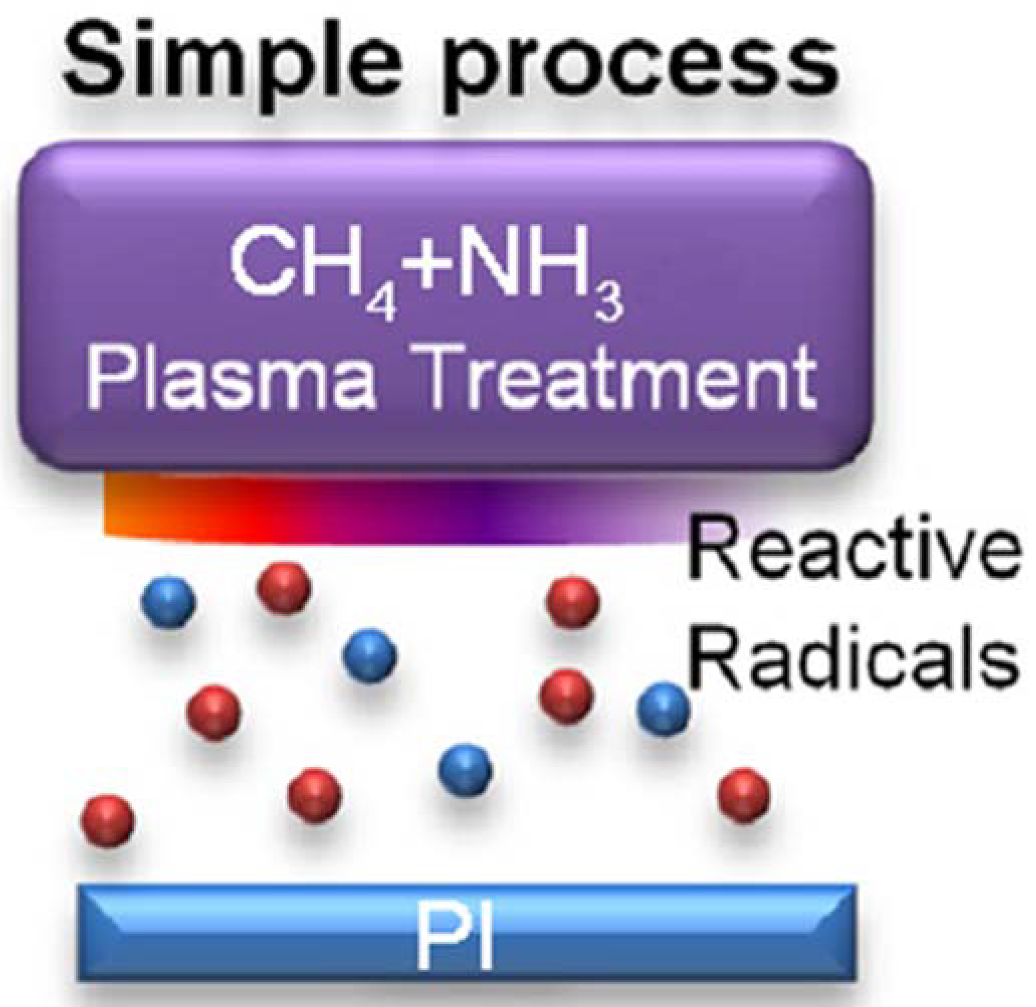
Figure 1. Schematic depicting the grafting of amino groups onto PI films by HWP treatment.
Preprints 80972 g001
Figure 2. OES profiles of the CH4/NH3 HWP discharge in the wavelength range of 200~800 nm.
Preprints 80972 g002
Figure 3. FE-SEM images of PI films under no treatment and plasma treatment at various Vs values: (a, b) no treatment; (c, d) 0 V; (e, f) –100 V; (g, h) –200 V; (i, j) –300 V; (k, l) –400 V; FE-SEM images of (m) a PI film under no treatment and (n) a PI film subjected to plasma treatment at a –Vs of 100 V after Cu plating.
Preprints 80972 g003
Figure 4. C 1s, O 1s, and N 1s XPS profiles of the PI films after no treatment and plasma treatment at various Vs values: (a) C 1s, no treatment; (b) C 1s, 0 V; (c) C 1s, –100 V; (d) C 1s, –200 V; (e) C 1s, –300 V; (f) C 1s, –400 V; (g) O 1s, no treatment; (h) O 1s, 0 V; (i) O 1s, –100 V; (j) O 1s, –200 V; (k) O 1s, –300 V; (l) O 1s, –400 V; (m) N 1s, no treatment; (n) N 1s, 0 V; (o) N 1s, –100 V; (p) N 1s, –200 V; (q) N 1s, –300 V; (r) N 1s, –400 V.
Preprints 80972 g004
Figure 5. XRD patterns of Cu-plated PI films with plasma treatment at various Vs values and without plasma treatment.
Preprints 80972 g005
Figure 6. (a) Surface roughness of the plasma-treated PI films at various times; (b) Surface roughness of PI films after plasma treatment and no treatment; (c) Peel strength between Cu films and PI films with various thicknesses after plasma treatment for various times and sputtering Cu plating; (d) Peel strength between Cu films with various thicknesses and PI films with various thicknesses after plasma treatment for 5 s and sputtering Cu plating; (e) Peel strength between Cu films with various thicknesses and PI films with various thicknesses after plasma treatment for 5 s and electroless Cu plating.
Preprints 80972 g006
Disclaimer/Publisher’s Note: The statements, opinions and data contained in all publications are solely those of the individual author(s) and contributor(s) and not of MDPI and/or the editor(s). MDPI and/or the editor(s) disclaim responsibility for any injury to people or property resulting from any ideas, methods, instructions or products referred to in the content.
Copyright: This open access article is published under a Creative Commons CC BY 4.0 license, which permit the free download, distribution, and reuse, provided that the author and preprint are cited in any reuse.
Prerpints.org logo

Preprints.org is a free preprint server supported by MDPI in Basel, Switzerland.

Subscribe

© 2024 MDPI (Basel, Switzerland) unless otherwise stated