1. Introduction
Three-dimensional (3D) vertically stackable structures are the mainstream in NAND flash memory. An increase in the word-line (WL) stack in 3D NAND is required to achieve high capacity and reduce bit costs [
1,
2,
3,
4]. The high-aspect-ratio (HAR) gate-all-around (GAA) polysilicon channel is effective in enhancing gate controllability and suppressing electrical fluctuations [
5,
6,
7,
8]. With GAA structures, triple-level and quadruple-level cells have been successfully commercialized in 3D NAND flash memory [
9,
10,
11,
12]. However, these multilevel operations are susceptible to threshold voltage (
VTH) variation because of the narrower margins in the programmed
VTH distribution compared with those of single-level cells [
13]. In addition, the HAR structure significantly increases process complexity, affecting electrical performance and reliability [
14,
15,
16,
17]. A tapered structure is typically observed in etched HAR holes, from top to bottom [
18,
19,
20,
21,
22,
23]. The tapered shape may primarily affect the program/erase (P/E) window of each cell along the WL string [
24,
25]. Simultaneously, a microtrench structure frequently forms close to the bottom region of the tapered etch hole. The cross-section of the microtrench generates a noncircular channel with spike-wise deformation, which can further degrade the uniformity of the electrical characteristics [
26,
27]. Although the electrical behavior of noncircular channel shape has been reported in some studies [
28], it is not clear how the spike affects electrical properties of the cell and how
VTH is determined by the spike. In this study, the distributions of trapped electrons and inversion electron density were investigated for noncircular cells with single or two spikes using Synopsys Sentaurus technology computer-aided design (TCAD). The channel current density and
VTH variations were correlated with the spike height and angle between spikes.
2. Simulation Structure and Methods
Figure 1a shows a schematic of the 3D NAND flash memory with three WL cells. The radial structure of a cell is composed of a metal gate, blocking oxide (BOX), charge trap layer (CTL), band-engineered tunneling layer (BE-TOX) consisting of O1/N1/O2, polysilicon (poly-Si) channel, and macaroni oxide.
Figure 1b,c,d show the cross-sectional schematics of the circular cell (C-cell), single-spike cell (SSC), and two-spike cell (TWSC), respectively. Parameter θ was introduced to analyze the effect of the distance between spikes in the TWSC cells, as shown in
Figure 1d. The height (H
Spike) and angle (θ) between the two spikes varied from 5 to 15 nm and 20° to 135°, respectively.
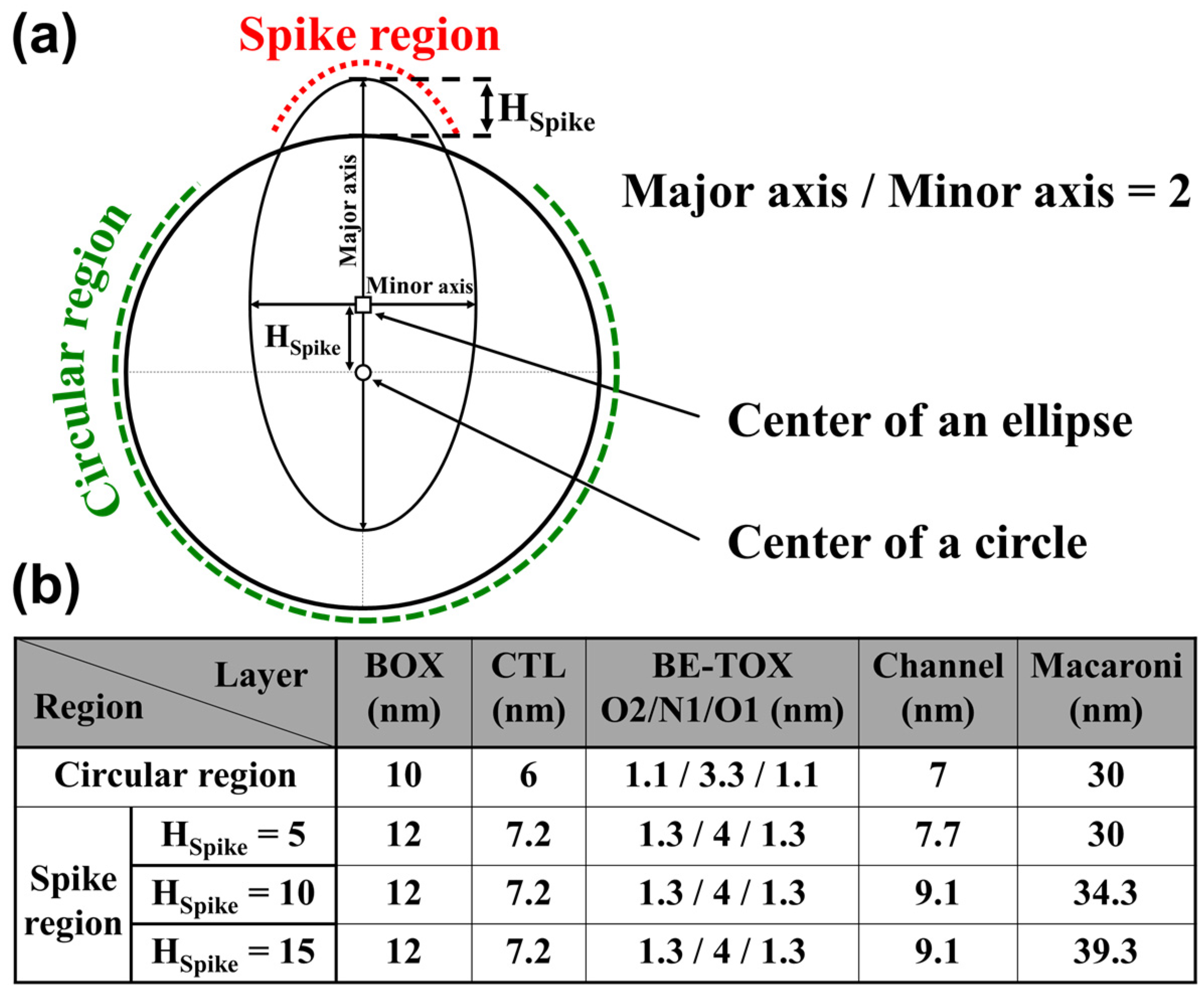
Figure 2 depicts a spike used in the simulation. The spike region was generated by overlapping a conventional circle and an ellipse, as shown in
Figure 2a. The center of the ellipse is away from the center of the circle by the H
Spike, inducing a spike shape in each layer, as shown in
Figure 2b. The thickness of each layer in spike region was set to be thicker than in circular region.
The Hurkx band-to-band tunneling model for gate-induced drain leakage, high-field-saturation mobility model in the channel were adopted. The quantum confinement effect was also incorporated to accurately analyze the channel current. The oxide layers in the BE-TOX and BOX layers were assumed to have no defects. Transient simulations with a nonlocal tunneling model were performed to simulate the P/E operation. Carriers in the CTL were transported according to the drift-diffusion model, and Shockley–Read–Hall (SRH) model was applied to the capture or emission of carriers into traps. The material properties of the CTL used in this study are listed in
Table 1. Silicon nitride has gaussian energy distribution for both electron and hole trap. The spatial distribution of the traps was set constant as we focused on the change in electrical properties due to the noncircular channel shape.
The program (PGM), erase (ERS), and read conditions were V
PGM = 16 V / t
PGM = 100 μs, V
ERS = −16 V / t
ERS = 1 ms,
VPASS = 5 V /
VBL = 0.05 V, respectively.
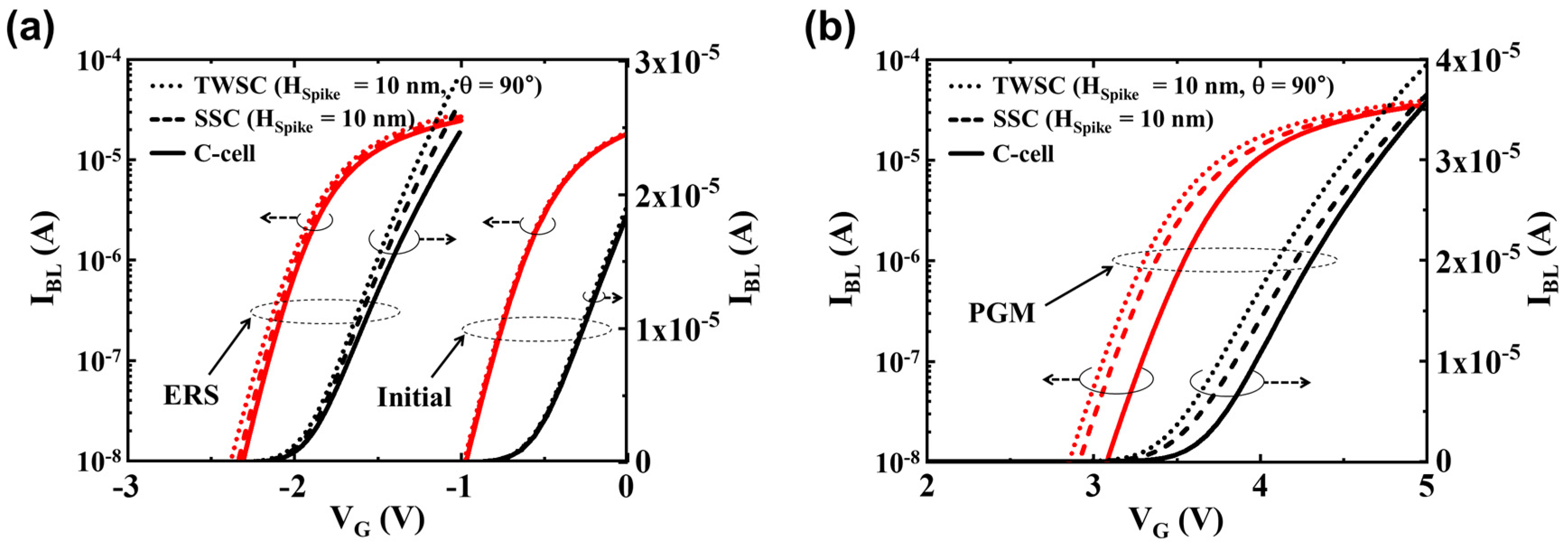
Figure 3 shows the bit-line current (
IBL) vs. gate voltage (
VG) curves of the C-cell and noncircular cells at the initial, ERS, and PGM states using 3D TCAD simulation.
VTH was extracted using an
IBL of 2
μA. The
VTH values of the C-cell were −0.5, −2, and 3.67 V in the initial, ERS, and PGM states, respectively. For the SSC and TWSC cells, the
VTH in the initial and ERS states were the same as or less different from
VTH in the C-cell as shown in
Figure 3a. However, in the PGM state, a negative shift of
VTH was clearly observed for noncircular cells, owing to structural deformation as shown in
Figure 3b. The SSC and TWSC cells were simulated with various H
Spike and θ values to further reveal their electrical behaviors.
3. Results and Discussions
3.1. SSC Characteristics
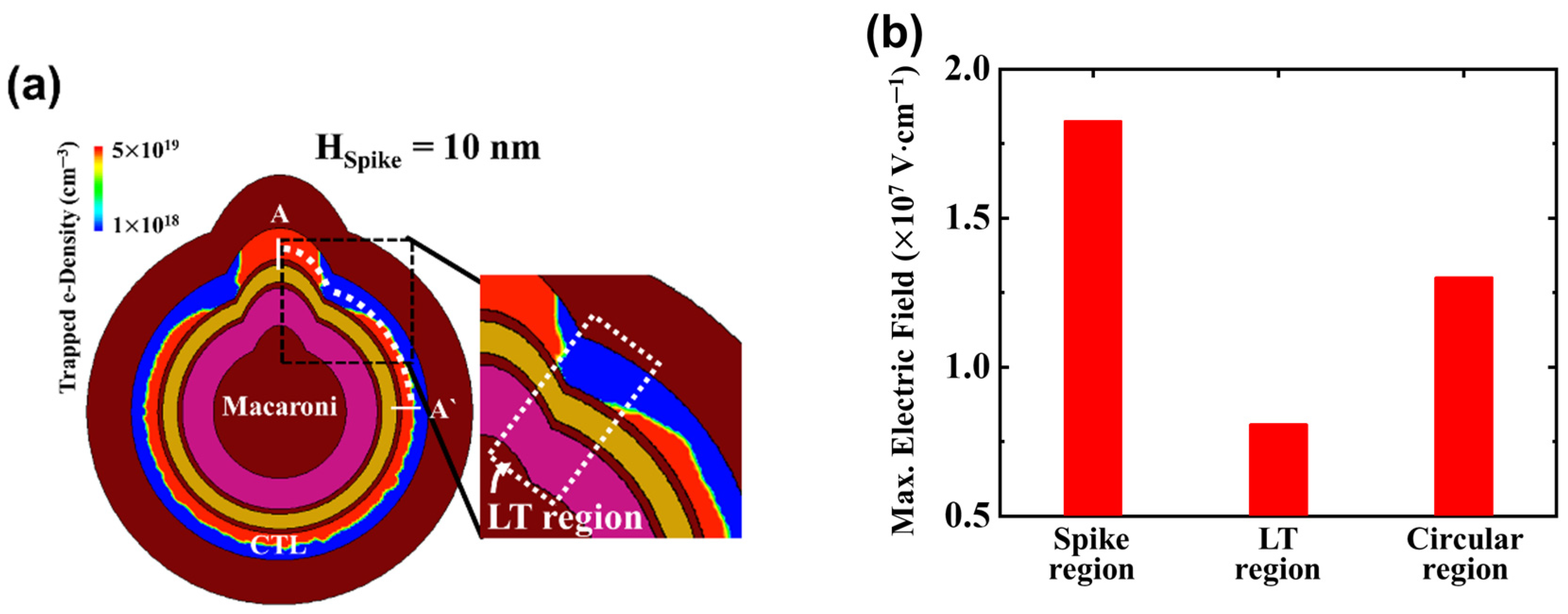
Figure 4a shows the distribution of the trapped electron density (e-density) in the CTL in the PGM state of the SSC. A gradual decrease in the e-density was observed in the region between the spike and circular regions. The less-trapped electron (LT) region is newly defined as where the e-density decreases by 10% of the circular region.
Figure 4b shows the maximum electric field (Emax) on the O1 layer of BE-TOX at V
PGM = 16 V in the SSC. The peak in the spike region showed the highest electric field compared with the LT and circular regions. The concave shape in the LT region could reduce Emax and induce smaller trapped charges in the LT region.
Figure 5a shows the distribution of the average trapped e-density in the PGM state along the A-A` perimeter with different H
Spike values. The average e-density was obtained by radially integrating the overall charge at each position in the CTL. For the C-cell, a uniform trapped e-density of 1.6 × 10
19 cm
−3 was obtained. For the SSC cell, a fully trapped electron of 5 × 10
19 cm
−3 was obtained in the spike region. As H
Spike increased, the minimum trapped e-density decreased, and the LT region expanded from 5.6 to 10 nm. The distribution of the trapped e-density depended on the H
Spike values, influencing the current flow in the channel and the corresponding
VTH values. A lower
VTH is associated with a reduction in the trapped e-density in the CTL of the circular structure. An increase in H
Spike lowered
VTH, although it increased the trapped e-density in the SSC, as shown in
Figure 5b.
Figure 6a shows the cross-sectional distribution of channel electrons in the SSC with H
Spike = 10 nm at
Vread =
VTH. Because the trapped e-density was high in the spike region, the inversion electron in that region was locally smaller than in other channel regions. However, the LT region had a smaller trapped e-density; thus, more channel electrons and a higher current density were induced.
Figure 6b shows the average channel e-density along the A-A` perimeter with different H
Spike values. The calculated channel e-density of the C-cell was as high as 4.6 × 10
16 cm
−3. The e-density peak coincided with the minimum trapped e-density in CTL (
Figure 5a). As H
Spike increased, the peak value increased from 1.6 × 10
17 to 2.1 × 10
17 cm
−3.
Figure 6c shows the ratio of the currents flowing in the three regions to the total channel current (at
Vread =
VTH) in the SSC in the PGM state. At H
Spike = 15 nm, the calculated normalized perimeter was as high as 70% for the circular region, 18% for the spike region, and 12% for the two LT regions, respectively. The intensity of current in the LT region became dominant with increasing H
Spike. For the SSC with H
Spike = 15 nm, 57% of the total current flowed through the two LT regions. During a PGM operation, a reduced electric field in the LT region induced a lower trapped e-density, which again increased the channel e-density.
3.2. TWSC Characteritsics
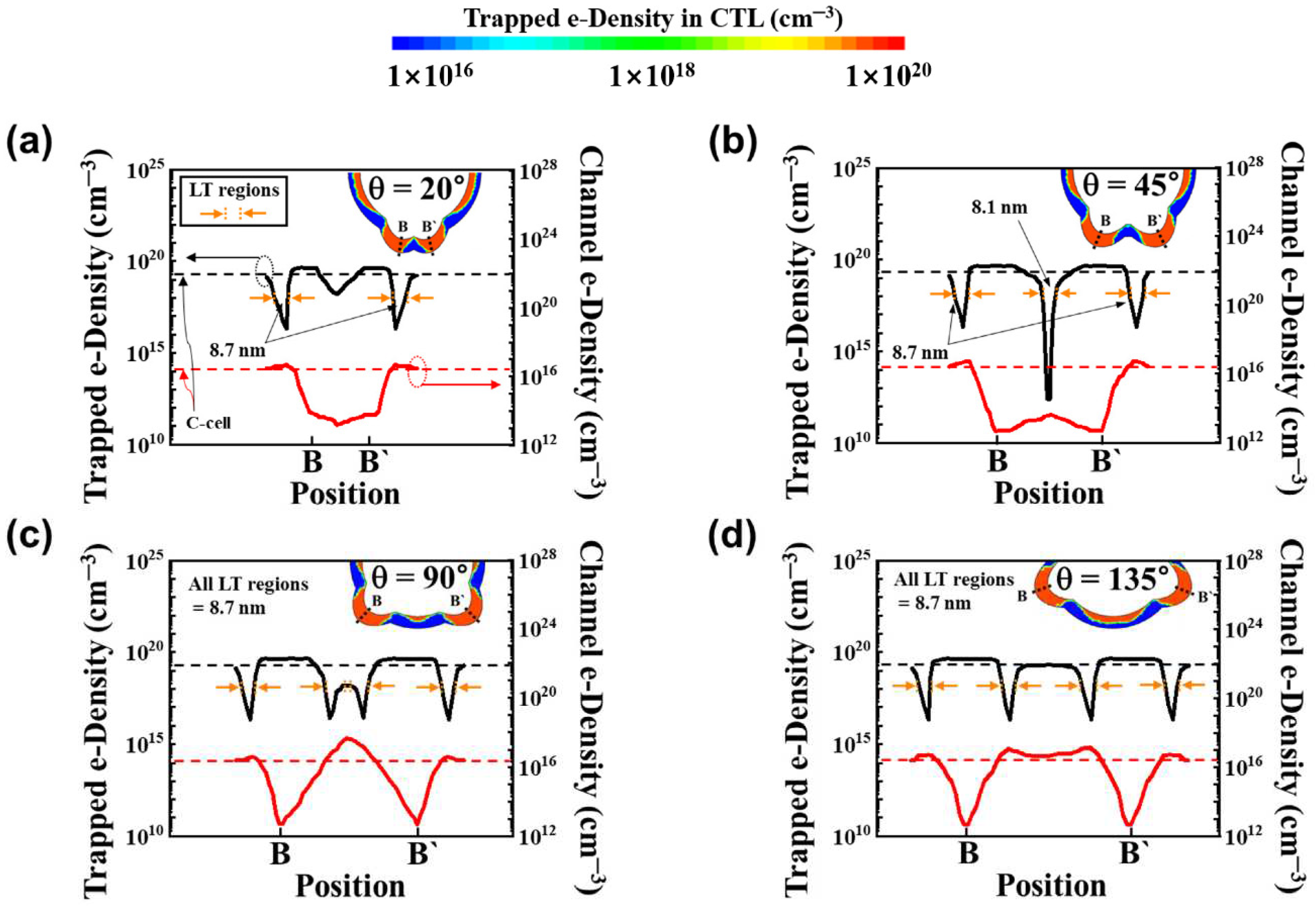
Figure 7 shows the distributions in the trapped e-density in CTL and channel e-density at
Vread =
VTH along the B-B` perimeter between two spikes in the PGM state. The angle between the spikes varied from 20° to 135° with H
Spike = 10 nm. The cross-sectional distribution of the trapped electrons in the CTL is shown in the insets. At θ = 135°, two LT regions were observed in the B-B' region where the minimum trapped e-density of 2.1 × 10
16 cm
−3 and the peak channel e-density of 1.3 × 10
17 cm
−3 (
Figure 7d). At θ = 90°, two LT regions were close and the minimum trapped e-density is unchanged, but peak channel e-density increased to 5 × 10
17 cm
−3 (
Figure 7c). As the angle decreased, the LT regions overlapped, and at θ = 45°, the LT region with the minimum trapped e-density of 2.5 × 10
12 cm
−3 and the peak channel e-density of 3 × 10
13 cm
−3 was formed (
Figure 7b). Both θ = 45° and θ = 20°, the B-B' region between two spikes showed a negligible electron density compared with the circular region, suggesting that the channel current mostly flowed through the circular region and the two LT regions outside B-B’ (
Figure 7a).
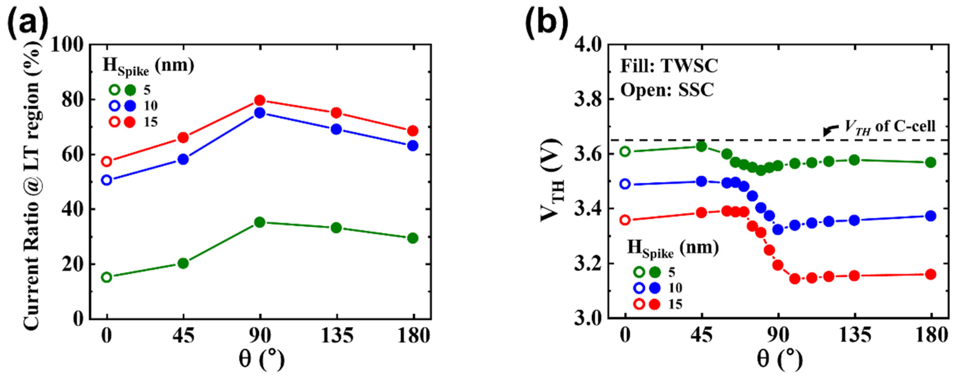
Figure 8a shows the current ratio flowing in the LT regions as functions of H
Spike and θ for the TWSCs. The channel current primarily flowed in the LT and circular regions and was lower than 1% in the spike regions. The current ratio was maximum at θ = 90°; it significantly increased with a high H
Spike value, increasing from 40% for H
Spike = 5 nm to 80% for H
Spike = 15 nm.
Figure 8b shows the
VTH variation for TWSCs with different H
Spike and θ values. The dashed line represents the
VTH value of the C-cell. All the SSCs and TWSCs showed a lower
VTH than the C-cell, and a higher spike induced a more significant decrease in
VTH. For the TWSC cells at approximately θ = 90°,
VTH reduction was observed because of the increased channel e-density at that angle (
Figure 7c).
4. Conclusions
We investigated the impact of a noncircular channel with spikes on the VTH characteristics using 3D TCAD simulations in vertical NAND flash memory. The region with lower trapped charges in the CTL between the spike and circular regions expanded as the spike height increased. SSCs and TWSCs showed lower VTH than the C-cell. In particular, for the TWSCs, the VTH variation became severe at θ = 90° as the spike height increased.
Author Contributions
Conceptualization, D.G., and J.W.K.; methodology, J.P., D.K., and G.S.Y.; writing-original draft preparation, D.G., J.K., and J.-S.L.; writing-review & editing, D.G., J.K., and J.-S.L.; supervision, J.-S.L.
Funding
This work was supported by National R&D Program through the National Research Foundation of Korea (NRF) funded by Ministry of Science and ICT (2020M3H2A1078045) and by Samsung POSTECH Research Center (SPRC) funded by Samsung Electronic.
Acknowledgments
The EDA tool was supported by the IC Design Education Center.
Conflicts of Interest
The authors declare no conflict of interest.
References
- K. Ishimaru, "Future of non-volatile memory-from storage to computing," in IEDM Tech. Dig., Dec. 2019, pp. 1.3.1–1.3.6, . [CrossRef]
- L. Heineck and J. Liu, "3D NAND Flash Status and Trends," ," in IEEE 14th Int. Memory Workshop (IMW), May 2022, pp. 1-4, . [CrossRef]
- J. Choe, "Memory Technology 2021: Trends & Challenges," 2021 International Conference on Simulation of Semiconductor Processes and Devices (SISPAD), 2021, pp. 111-115, . [CrossRef]
- R. Shirota, "3D-NAND flash memory and technology," in Proc. Adv. Non-Volatile Memory Storage Technol., Jan. 2019, pp. 283–319, . [CrossRef]
- J. Y. Seo, Y. Kim, S. H. Park, W. Kim, D.-B. Kim, J.-H. Lee, H. Shin, and B.-G. Park, "Investigation into the effect of the variation of gate dimensions on program characteristics in 3D NAND flash array," 2012 IEEE Silicon Nanoelectronics Workshop (SNW), 2012, pp. 1-2, . [CrossRef]
- Silvagni, "3D NAND Flash Based on Planar Cells," Computers, vol. 6, no. 4, p. 28, Oct.2017.
- Goda, "3-D NAND Technology Achievements and Future Scaling Perspectives," in IEEE Trans. Electron Devices, vol. 67, no. 4, pp. 1373-1381, April 2020, . [CrossRef]
- S. Barraud et al., "7-Levels-Stacked Nanosheet GAA Transistors for High Performance Computing," 2020 IEEE Symp. VLSI Technol., 2020, pp. 1-2, . [CrossRef]
- S. Liang et al., "An Empirical Study of Quad-Level Cell (QLC) NAND Flash SSDs for Big Data Applications," 2019 IEEE International Conference on Big Data (Big Data), 2019, pp. 3676-3685, . [CrossRef]
- N. Papandreou et al., "Reliability of 3D NAND flash memory with a focus on read voltage calibration from a system aspect," 2019 19th Non-Volatile Memory Technol. Symp. (NVMTS), 2019, pp. 1-4, . [CrossRef]
- N. Papandreou et al., "Characterization and Analysis of Bit Errors in 3D TLC NAND Flash Memory," 2019 IEEE Int. Rel. Phys. Symp. (IRPS), 2019, pp. 1-6, . [CrossRef]
- K. Mizoguchi, T. Takahashi, S. Aritome, and K. Takeuchi, "DataRetention Characteristics Comparison of 2D and 3D TLC NAND Flash Memories," in 2017 IEEE International Memory Workshop (IMW), pp. 1–4.
- M. Fukuchi, S. Suzuki, K. Maeda, C. Matsui and K. Takeuchi, "BER Evaluation System Considering Device Characteristics of TLC and QLC NAND Flash Memories in Hybrid SSDs with Real Storage Workloads," 2021 IEEE Int. Symp. Circuits and Systems (ISCAS), 2021, pp. 1-4, . [CrossRef]
- T. Reiter, X. Klemenschits and L. Filipovic, "Impact of plasma induced damage on the fabrication of 3D NAND flash memory," Solid-State-Electron., vol. 192, 2022, 108261.
- J. Kang et al., "Highly Reliable Cell Characteristics with CSOB(Channel-hole Sidewall ONO Butting) Scheme for 7th Generation 3D-NAND," 2021 IEEE International Electron Devices Meeting (IEDM), 2021, pp. 10.1.1-10.1.4, . [CrossRef]
- Y. -A. Chung et al., "Study of Plasma Arcing Mechanism in High Aspect Ratio Slit Trench Etching," 2019 30th Annual SEMI Advanced Semiconductor Manufacturing Conference (ASMC), 2019, pp. 1-4, . [CrossRef]
- K. Parat and A. Goda, "Scaling Trends in NAND Flash," 2018 IEEE International Electron Devices Meeting (IEDM), 2018, pp. 2.1.1-2.1.4, . [CrossRef]
- Goda and K. Parat, "Scaling directions for 2D and 3D NAND cells," in IEDM Tech. Dig., Dec. 2012, pp. 2.1.1–2.1.4, . [CrossRef]
- H. Kim, S. -J. Ahn, Y. G. Shin, K. Lee and E. Jung, "Evolution of NAND Flash Memory: From 2D to 3D as a Storage Market Leader," 2017 IEEE Int. Memory Workshop (IMW), 2017, pp. 1-4, . [CrossRef]
- Y. Yanagihara, K. Miyaji and K. Takeuchi, "Control Gate Length, Spacing and Stacked Layer Number Design for 3D-Stackable NAND Flash Memory," 2012 4th IEEE Int. Memory Workshop, 2012, pp. 1-4, . [CrossRef]
- K. Ko, J. K. Lee and H. Shin, "Variability-Aware Machine Learning Strategy for 3-D NAND Flash Memories," in IEEE Trans. Electron Devices, vol. 67, no. 4, pp. 1575-1580, April 2020, . [CrossRef]
- U. M. Bhatt, S. K. Manhas, A. Kumar, M. Pakala and E. Yieh, "Mitigating the Impact of Channel Tapering in Vertical Channel 3-D NAND," in IEEE Trans. Electron Devices, vol. 67, no. 3, pp. 929-936, March 2020, . [CrossRef]
- J. G. Lee, W. J. Jung, J. H. Park, K. -H. Yoo and T. W. Kim, "Effect of the Blocking Oxide Layer With Asymmetric Taper Angles in 3-D NAND Flash Memories," in IEEE Journal of the Electron Devices Society, vol. 9, pp. 774-777, 2021, . [CrossRef]
- K. T. Kim, S. W. An, H. S. Jung, K. Yoo and T. W. Kim, "The Effects of Taper-Angle on the Electrical Characteristics of Vertical NAND Flash Memories," in IEEE Electron Device Lett., vol. 38, no. 10, pp. 1375-1378, Oct. 2017, . [CrossRef]
- U. M. Bhatt, S. K. Manhas, A. Kumar, M. Pakala, and E. Yieh, "Mitigating the impact of channel tapering in vertical channel 3-D NAND," in IEEE Trans. Electron Devices, vol. 67, no. 3, pp. 929–936, Mar. 2020.
- P. Nowakowski, M. Ray, P. Fischione and J. Sagar, "Top-down delayering by low energy, broad-beam, argon ion milling — a solution for microelectronic device process control and failure analyses", 28th Annual SEMI Advanced Semiconductor Manufacturing Conference (ASMC), 2017, pp. 95-101.
- Han, Z. Wu, C. Yang, L. Xie, B. Xu, L. Liu, Z. Yin, L. Jin and Z. Huo, "Influence of accumulated charges on deep trench etch process in 3D NAND memory,” Semicond. Sci. Technol., vol. 35, no. 4, 2020, Art. no. 045003, . [CrossRef]
- Fayrushin, H. Liu, A. Mauri, G. Carnevale, H. Cho and D. Mao, "Numerical Study of Non-Circular Pillar Effect in 3D-NAND Flash Memory Cells," 2019 IEEE Workshop on Microelectronics and Electron Devices (WMED), 2019, pp. 1-4, . [CrossRef]
|
Disclaimer/Publisher’s Note: The statements, opinions and data contained in all publications are solely those of the individual author(s) and contributor(s) and not of MDPI and/or the editor(s). MDPI and/or the editor(s) disclaim responsibility for any injury to people or property resulting from any ideas, methods, instructions or products referred to in the content. |
© 2023 by the authors. Licensee MDPI, Basel, Switzerland. This article is an open access article distributed under the terms and conditions of the Creative Commons Attribution (CC BY) license (http://creativecommons.org/licenses/by/4.0/).

