1. Introduction
The remarkable progress in wide bandgap AlGaN semiconductor materials has garnered significant interest since the 1980s. This interest has been fueled by emerging research needs in device growth processes and the need for high-power, cost-effective, environmentally safe, and resistant to both high temperatures, as well as to high radiations [
1,
2]. AlGaN-based semiconductors have been emerged as a highly promising candidates for the production of intelligent and eco-friendly ultraviolet-B (UVB) and deep ultraviolet (DUV) emitters that meet the desires of the Minamata Convention of 2020 and the 17 sustainable development goals (17 SDGs) of the United Nations (UN) [
2,
3]. High-power AlGaN-based DUV LEDs hold a significance role for a wide range of medical and agricultural applications [
3]. These include sterilization uses, water and air purification, as well as for wide range of medical applications [
4]. Furthermore, we have been consistently coexisted with numerous infectious diseases caused by viruses, bacteria, and fungus during the human civilization. The emergence of the Severe Acute Respiratory Syndrome Coronavirus 2 (SARS-CoV-2) has not only had a significant impact on human health, but also significantly influenced the global economy and people’s ways of life [
5,
6]. Therefore, the control of infectious diseases has become a pressing global concern for human society, both in the present and in the distant future as well as in the terrestrial life too. In particular, clean UV technologies offer a potential solution to mitigate the impact of novel viral pandemics everywhere including in the space station. In this regard, recently several research projects have been demonstrated at the emissions wavelengths of 222 nm and 254 nm, respectively and found to be more effective in combating pathogen contamination, whether in manned or unmanned environments [
5,
7]. Meanwhile, in America, Japan, Germany and Canada, UVB and far-UVC devices are currently employed for the clinical treatment of infected wounds and skin issues [
3,
7]. There is a growing need to investigate environmentally friendly and safe wide bandgap materials for the epitaxial growth of UV emitters structure and fabrication of UV LED modules. Among such safe and wide bandgap materials the epitaxial growth of UV emitters on AlN templates is one of the most promising choice [
2].
AlGaN-based UV LEDs are facing several challenges, such as low internal-quantum efficiency (IQE) due to a high level of threading dislocation densities (TDDs) [
3,
8], due to a high level of UV light loss in p-GaN contact layer [
9], high operating voltages [
3,
9,
10]. Furthermore, low wall-plug efficiency (WPE) due to the low IQE as well as efficiency droop, poor light extraction efficiency (LEE) caused by dominant transverse magnetic (TM)-polarized light emission instead of transverse electric (TE)-polarized light emission are the remaining challenges [
11]. Poor hole injection toward the quantum-well is serious issue caused by the low density of hole in p-type AlGaN hole source layer (HSL), and also parasitic radiative recombination rate attributed to the asymmetric injection of electron and hole toward the quantum-well [
5,
8,
12]. In addition, large lattice mismatch and high polarization charge density in Al-rich AlGaN induces the quantum confinement stark effect (QCSE) which leads to reduction of overlapping of electron-hole wavefunction in the active region [
13,
14]. One central issue is the low hole injection efficiency from the p-side towards the MQWs and high operating voltages of AlGaN-based UV LEDs and LDs [
3,
8,
10]. All these issues are resulting in poor external-quantum efficiency (EQE) and low light output power (LOP) of DUV LEDs, when compared to the blue brethren LED [
2]. The issue of low hole injection in the DUV LED has been triggered by high activation energy of Mg atoms in the fixed Al-contents of AlGaN (approximately 200 meV in GaN, reaching up to approximately 630 meV in AlN), low solubility of Mg-atoms in p-AlGaN HSL, compensation by nitrogen vacancies, the formation of Mg-H complexes, and the presence of unwanted impurities such as hydrogen (H), oxygen (O), and carbon (C) in the p-AlGaN HSL and p-AlGaN contact layer [
15].
To effectively control and manipulate the carrier’s injection behavior, an extensive research effort has been made to optimize the energy band structures of AlGaN-based DUV LEDs [
16]. One effective approach to address efficiency-droop in AlGaN-based DUV LEDs involves the incorporation of a undoped Al-graded from high aluminum (Al) composition to low level of composition in the single layered electron-blocking structure, which can significantly mitigate the issue without requiring a Mg-doped multi-quantum-barrier electron-blocking-layer (p-MQB EBL) [
17]. The polarization-induced 3D hole generation technique represents a promising solution for achieving improved current injection efficiency [
2,
17,
18]. Khan et al., reported about the 254 nm DUV LEDs grown in MOCVD, where the donor– acceptor pair (DAP)-like emission peak centered at 301 nm was successfully suppressed but encountered with high operating voltages as well as efficiency droop [
19]. Among the various approaches being explored, the utilization of N-polar AlGaN alloys as the fundamental elements for DUV LEDs is gaining significant attention in the III-nitride research community [
20]. However, based on current knowledge, the maximum reported EQE for AlGaN-based UVB LED stands at 9.6% at emission wavelength of 304 nm, UVC LEDs stands at 20% at emission wavelength of 275 nm [
2,
21]. For DUV LEDs emitting wavelengths below 260 nm, the EQE typically falls within the range of 1.2-2.2% [
19,
22,
23,
24] however all these devices suffered from efficiency droops and high contact resistances. Achieving DUV LEDs with wavelengths below 260 nm requires an Al composition of around 64 -78% in the AlGaN material [
19,
25]. The tunnel junction (TJ)-based UV LED, operated at an injection current of 40 mA, at emission wavelength of 273 nm exhibited a significantly reduced turn-on voltage (V
th) from 12 V to 5.8 V, along with an enhanced IQE from 30% to 45%. The DUV LED still achieves a considerable boost in LOP of 173.3% at current density of 60 A/cm
2, however it suffered from the efficiency droop of 11.23% [
26]. The n-AlGaN-based tunneling assisted layer in DUV LED has achieved a maximum IQE of 62%, with an efficiency droop of 15% [
5]. Recently, the simulation results indicate that TJ-based LED at 254 nm wavelength exhibit a significant enhancement in the IQE of approximately 82% with a minimal efficiency droop of 3% at an intensity of 200 A/cm
2 [
27]. However, there is no report about the zero efficiency droop and highly low operating voltages in the TJ-based DUV LED at emission wavelength of 254 nm [
19,
27].
In order to address these outsatnding challenges, we have strategically incorporated AlGaN-based TJ into the polar DUV LEDs, resulting in what we refer to as TJ-LEDs. Our research demonstrates that the 254 nm-band TJ-LEDs surpass conventional polar LEDs in several aspects after optimization of both dopant levels as well as structural thicknesses of the new TJ. The new devices exhibited enhanced IQE, higher LOP, reduced efficiency droop, low differential resistance, lower turn-on voltage, and decreased parasitic recombination rate. One of the notable advantages of the AlGaN-based TJ-LED studied in this work is its ability to maintain excellent electrical and optical properties even at a low p-type doping level in the TJ. This unique characteristic offers a novel approach to enhance the performances of experimental DUV LED devices, which is attributed to the high hole injection toward the MQWs and low Auger recombination rate. The underlying mechanisms behind the improvement facilitated by the TJ are analyzed through numerical studies, providing a valuable insights for future optimization of experimental N-polar AlGaN-based DUV emitters.
2. Simulation Parameters
The numerical investigations into the electrical and optical properties of both DUV LEDs (Conventional and TJ-based) were carried out by using Advance Physical Models of Semiconductor Devices (APSYS) provided by Crosslight Inc [
28]. The energy band alignments of the DUV LEDs are calculated by using the 6×6 k.p model [
29]. The bandgap of GaN and AlN are set to be 3.4 eV and 6.2 eV respectively [
30]. The bowing parameter and band offset ratio of the AlGaN MQWs are assumed to be 0.94 eV and 0.3/0.7, respectively [
31]. The Mg activation energy in p-AlGaN HSL is scaled linearly from 170 meV (GaN) to 670 meV (AlN) [
32]. The back loss is assumed to be 2400 m
-1 for 300 μm × 300 μm size LED chip [
33]. The Shockley Read-Hall (SRH) recombination lifetime, the Auger coefficient, and the radiative recombination coefficient are set as 10 ns, 1×10
-30 cm
3/s, and 2.13×10
-11 cm
3/s, respectively [
26]. In addition, a 50% polarization screening factor is considered to result from the screening effect caused by dislocations, defects, and other interface charges [
24]. In the APSYS, the quantum-well (QW) k. p band theory including stress effects together with the self-consistent computational model of QW are used to calculate the IQE and further details can be found elsewhere [
28]. Besides, the used tunneling model of APSYS in this work, we also follow the derivation of band-to-band tunneling current as prescribed in Ref [
35]. With a combination of the drift-diffusion model, we could possibly extract the carrier generation and distribution when the TJ-based LED is under operation [
26]. Other material parameters used in this work can be found elsewhere too [
36].
3. AlGaN-based DUV LED Devices Structures
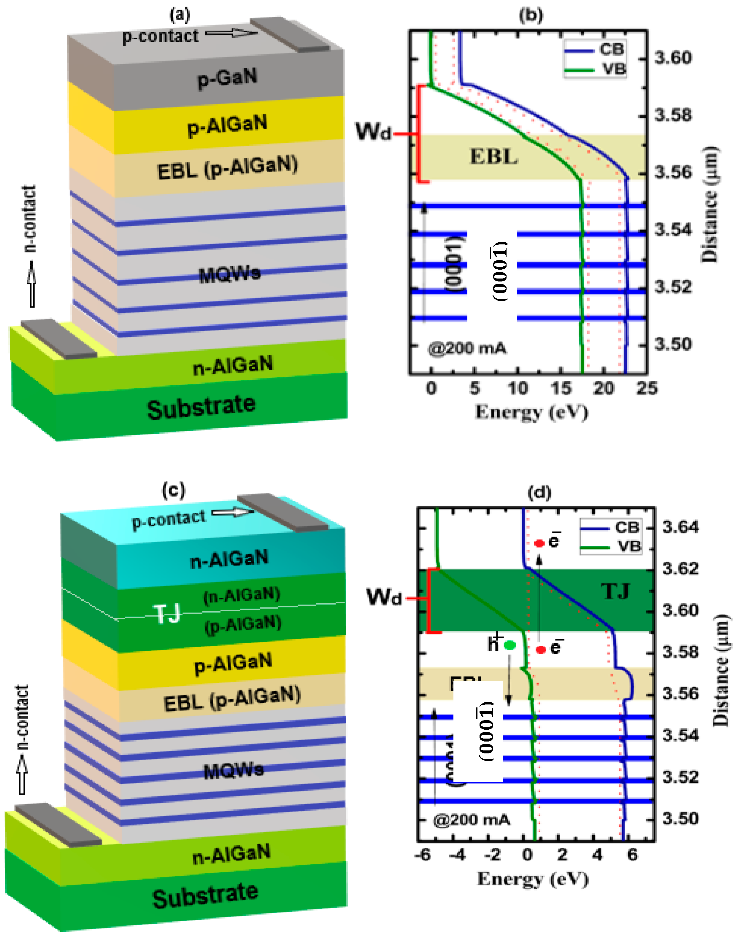
In this work, two different types of LEDs structures are investigated via simulations: the conventional LED (C-LED) and tunnel junction-based LED (TJ-LED). The whole devices are grown in N-polar direction
). The C-LED structure is considered on AlN template on c-sapphire substrate, as shown in
Figure 1a. The 3.5 μm thick n-Al
0.68Ga
0.32N electron source layer (ESL) has been doped with Si atomic concentration of 5.0×10
18 cm
-3. The MQWs of both C-LED and TJ-LED consist of five pairs of 2 nm-thick undoped Al
0.65Ga
0.35N quantum-wells (QWs) and 8 nm-thick undoped Al
0.75Ga
0.25N quantum-barriers (QBs), with the Al composition tailored for an emission wavelength of 254 nm, as shown in
Figure 1a,c. A 15 nm- thick p-Al
0.90Ga
0.10N electron-blocking layer (EBL) doped with Mg concentration of 1.5×10
19 cm
-3, while the 18 nm-thick p-Al
0.7Ga
0.30 N hole source layer (HSL) doped with Mg concentration of 1×10
19 cm
-3 and followed by 20 nm-thick p-GaN (Mg: 5×10
19 cm
-3) layer as a p-contact of the C-LED only. The relevant energy band diagram of the C-LED is shown in
Figure 1b.
Figure 1.
Schematic structures of N-polar (a) C-LED, (b) Energy band diagram of C-LED, (c) Schematic structure N-polar TJ-LED and (d) Energy band diagram of the N-polar TJ-Based DUV LED under 200 mA current drive.
Figure 1.
Schematic structures of N-polar (a) C-LED, (b) Energy band diagram of C-LED, (c) Schematic structure N-polar TJ-LED and (d) Energy band diagram of the N-polar TJ-Based DUV LED under 200 mA current drive.
The main difference between the C-LED and TJ-LED devices lies in the p-type side including contact-layer beyond the EBL. A conventional 20 nm p-GaN contact-layer was utilized for the C-LED with a p-type Ohmic contact on the top. For TJ-LED a 15 nm-thick p-Al
0.75Ga
0.25N layer (Mg: 1×10
18 cm
-3) and a 15nm-thick n-Al
0.75Ga
0.25N Layer (Si: 1×10
18 cm
-3) of TJ followed by 50 nm-thick n-Al
0.64Ga
0.36N (Si: 5×10
18 cm
-3) p-contact layer are used, as shown in
Figure 1c. The relevant energy band diagram of the TJ-LED is shown in
Figure 1d, where TJ layer has been shown in a clear manner with highlighted portion. Both the the energy band diagrams of C-LED and TJ-LED are taken at the same injection current of 200 mA.
In
Figure 1b,d the depletion width (
) is extracted from the band energies of both LEDs structures which is an important part for specifying the carrier quantum tunneling. The relationship between the tunneling probability (
) and W
d is expressed in Equation (1) [
10,
27].
where in equation (1),
stands for the tunnelling probability,
represent the width of tunnelling layer,
is the energy bandgap,
h is the Plank‘s constant and
is the carrier effective mass. The narrow is the width of depletion layer the higher will be the tunneling probability of carriers and better will be the performance of the DUV LED devices. It is clearly observed from
Figure 1d that after insertion of the TJ layer the
is reduced which may leads to high quantum tunneling phenomenon. As a result quite high IQE as well as low differential resistance can be achived. We also optimized both the doping level and structural thickness of the TJ in the DUV LED and quite low operating voltages were obtained. The performance parameters along with carrier injection variation are investigated and compared for both LED devices in the next section.
4. Results and Discussion
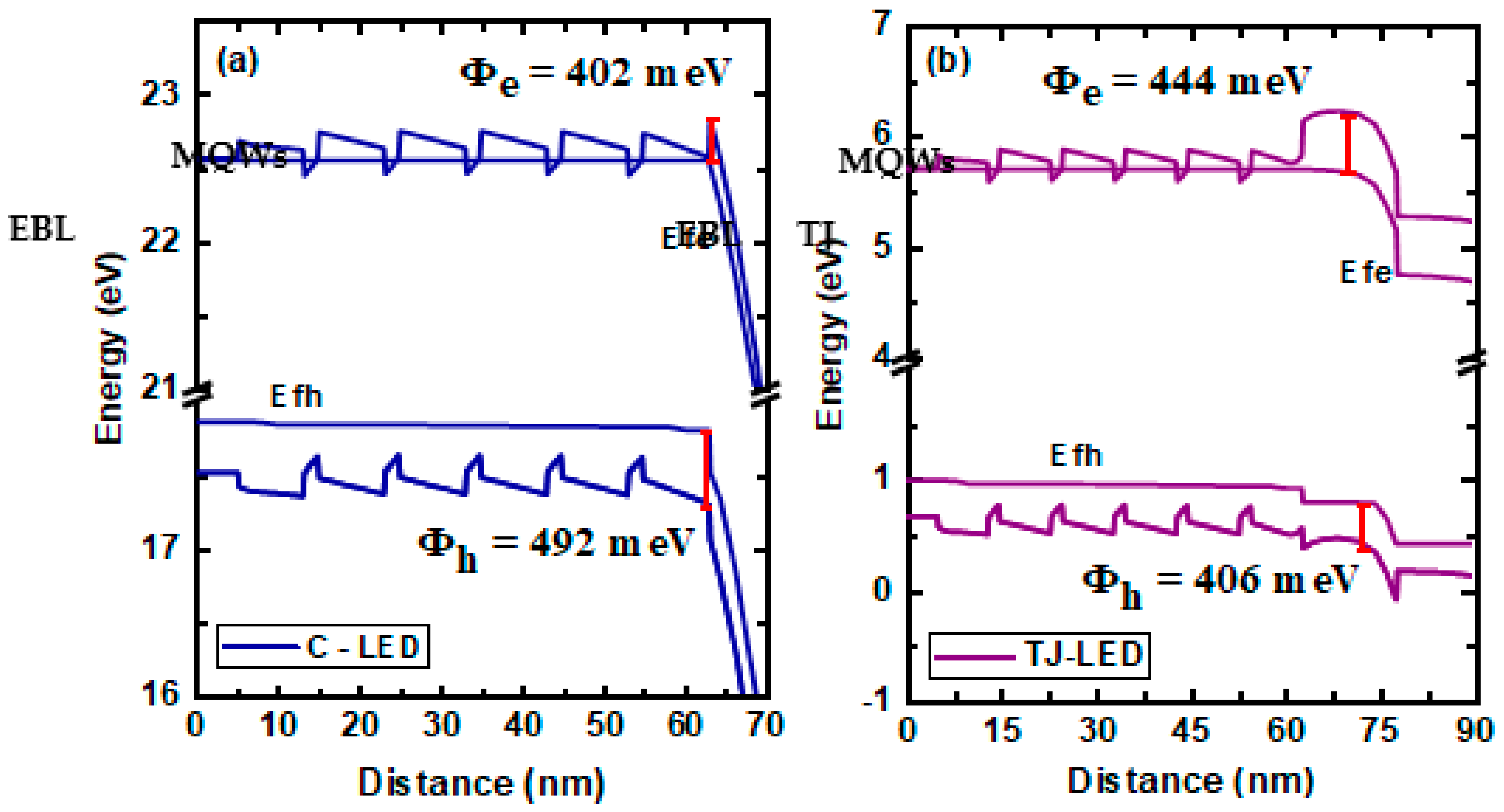
To comprehend the functionalities of the optimized AlGaN-based TJ in N-polar DUV LED, we performed the energy band structure analysis of the two devices, as shown in
Figure 2a,b.
Figure 2a,b give the energy band diagrams and quasi-Fermi level of electrons and holes (E
f(e,h)) in both C-LED and TJ-LED at an injection current of 200 mA. As demonstrated in
Figure 2b, a 30 nm-thick p-Al
0.75Ga
0.25N/n-Al
0.75Ga
0.25N TJ can be formed in the TJ-LED. The conduction band barrier height (𝜱
e) and valance band barrier height 𝜱
h for both device structures are calculated, as show in
Figure 2b–b. The value of 𝜱
e in the TJ-LED is increased up to 444 meV, when compared to the value of 𝜱
e around 402 meV in C-LED. It is showing that the value of 𝜱
e around 42 meV in TJ-LED is increased, which can effectively block an electron leakage. Conversely, the value of 𝜱
h in the TJ-LED is decreased up to 406 meV, when compared to the value of 𝜱
h around 492 meV in C-LED. It is showing that the value of 𝜱
h around 86 meV in TJ-LED is decreased, which can effectively enhance the hole injection toward the MQWs. From the band alignment it can been seen that TJ help to lower the energy alignment from the higher state that create better opportunity for 𝜱
h reduction. In comparison, it can be concluded that 𝜱
e of TJ-based LED is increased and 𝜱
h of the TJ-LED is decreased due to the p-Al
0.75Ga
0.25N/n-Al
0.75Ga
0.25N TJ layer optimization. The improved 𝜱
e can effectively block the electron overflow into p-region and significantly reduces the non-radiative recombination rate including Auger recombination rate (A.R.R), which is the main cause of IQE droop at higher injection current [
3]. Similarly, the lowered 𝜱
h can effectively promote hole injection from p-region toward MQWs and significantly contribute to the radiative recombination rate, which is the main reason of high IQE in the TJ-LED [
7]. These findings suggest that the proposed TJ-LED structure not only induced the quantum tunneling phenomena but it can also improve the carrier injection efficiency by manipulating 𝜱
e and 𝜱
h without sacrificing energies barriers supremacy.
Figure 2.
Energy Band Profile at EBL region of N-polar (a) C-LED and (b) TJ-LED.
Figure 2.
Energy Band Profile at EBL region of N-polar (a) C-LED and (b) TJ-LED.
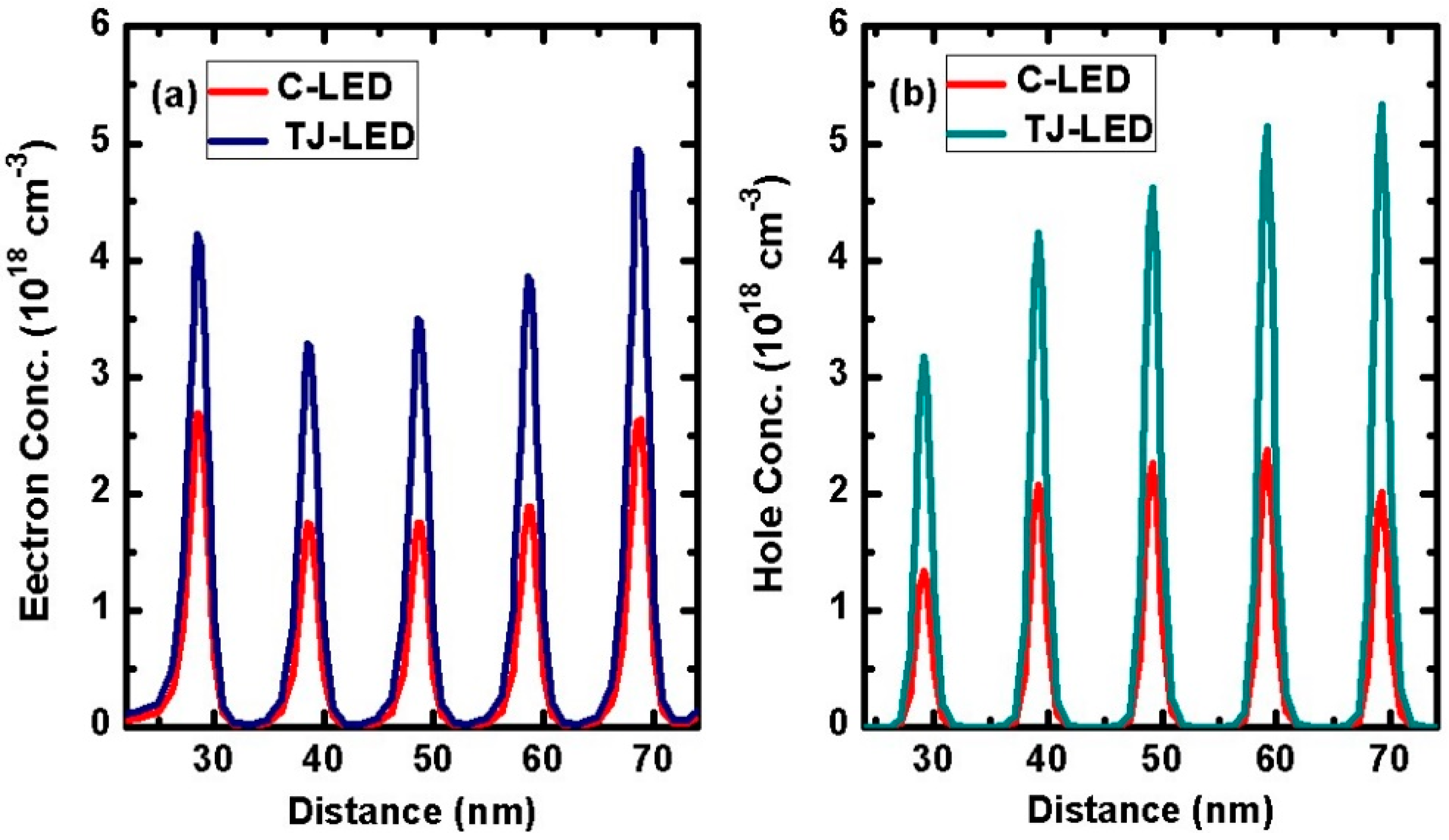
To unveil the improved carrier injection efficiency facilitated by the TJ, we explored the behaviours of carriers (electrons and holes) in the active regions of both the LED devices.
Figure 3a–b depicts the electron and hole concentration distribution in the MQWs of C-LED and TJ-LED at 200 mA injection current, respectively. The carrier concentration, especially the hole concentration in the MQWs of TJ-LED has been significantly improved, shown in
Figure 3b. It can increase the radiative recombination rate in each QW of TJ-LED which helps to generate more output power, and thus reducing the differential resistances of the newly designed TJ-LED. This indicates that the specially designed TJ can effectively modulate the carrier transport behaviour from the n- and p-type carrier injection layer into the active region by both quantum tunnelling effect and carrier diffusion transport.
Figure 3.
Profiles of (a) electron concentration, (b) hole concentration in the MQWs of both LEDs.
Figure 3.
Profiles of (a) electron concentration, (b) hole concentration in the MQWs of both LEDs.
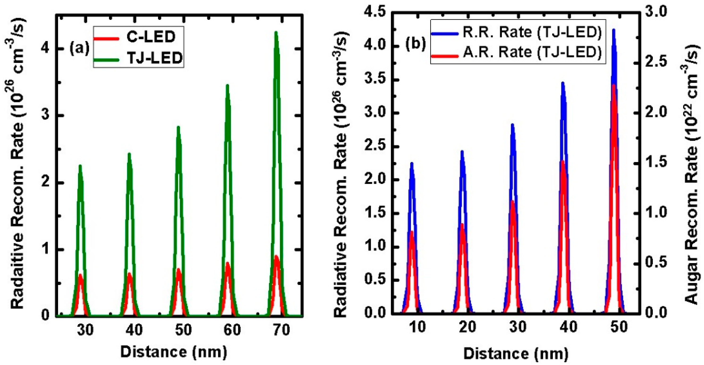
The radaiative recombination rate (R. R. R) and Auger recombination rate (A. R. R) are investigated in
Figure 4a,b to see the scenario of IQE in the new design structure of TJ-based DUV LED. It is observed that the higher hole concentration in the MQWs of the TJ-LED significantly affects the radiative recombination rate, when compared to the C-LED. The radiative recombination rate of TJ-LED is found to be four-time higher than the radiative recombination rate of C-LED, which confirms the superior feature of the newly designed TJ-based DUV LED. It also confirms that the specially designed TJ in the AlGaN-based DUV LED can simultaneously improve the hole injection toward the MQWs and suppress the electron leakage from the MQWs toward the p-side. Ultimately leading to the largely increased carrier concentration and recombination rate in the active region and subsequently significantly enhance to the optical and electrical characteristics of the TJ-based DUV LED [
37].
Figure 4b showing the comparison between radiative recombination and auger recombination rates of TJ-LED. The radiative recombination rates was found quite larger than the auger recombination rates of TJ-LED at 254 nm emission wavelength, shown in
Figure 4b. The auger recombination is the part of non-radiative recombination and it cannot be ignored when designing the active region of the DUV LED, and it has been identified as one of the main reason for efficiency rollover or droop in the III-nitride based devices at high injection current levels [
38]. The significantly reduced auger recombination rate of TJ-LED may lead to the zero efficiency droop, as shown in
Figure 6a.
Figure 4.
(a) Radiative recombination rate (R. R. R) rate in the MQWs of both LEDs and (b) comparison of radiative recombination rate (R. R. R) in unit of 1026 cm-3/s and Auger recombination rate (A. R. R) in unit of 1022 cm-3/s of TJ-LED in active region.
Figure 4.
(a) Radiative recombination rate (R. R. R) rate in the MQWs of both LEDs and (b) comparison of radiative recombination rate (R. R. R) in unit of 1026 cm-3/s and Auger recombination rate (A. R. R) in unit of 1022 cm-3/s of TJ-LED in active region.
The effect of carrier injection efficiency improvement is explored further by comparing the calculated optoelectronic characteristics of studied LEDs structures in
Figure 5 and
Figure 6.
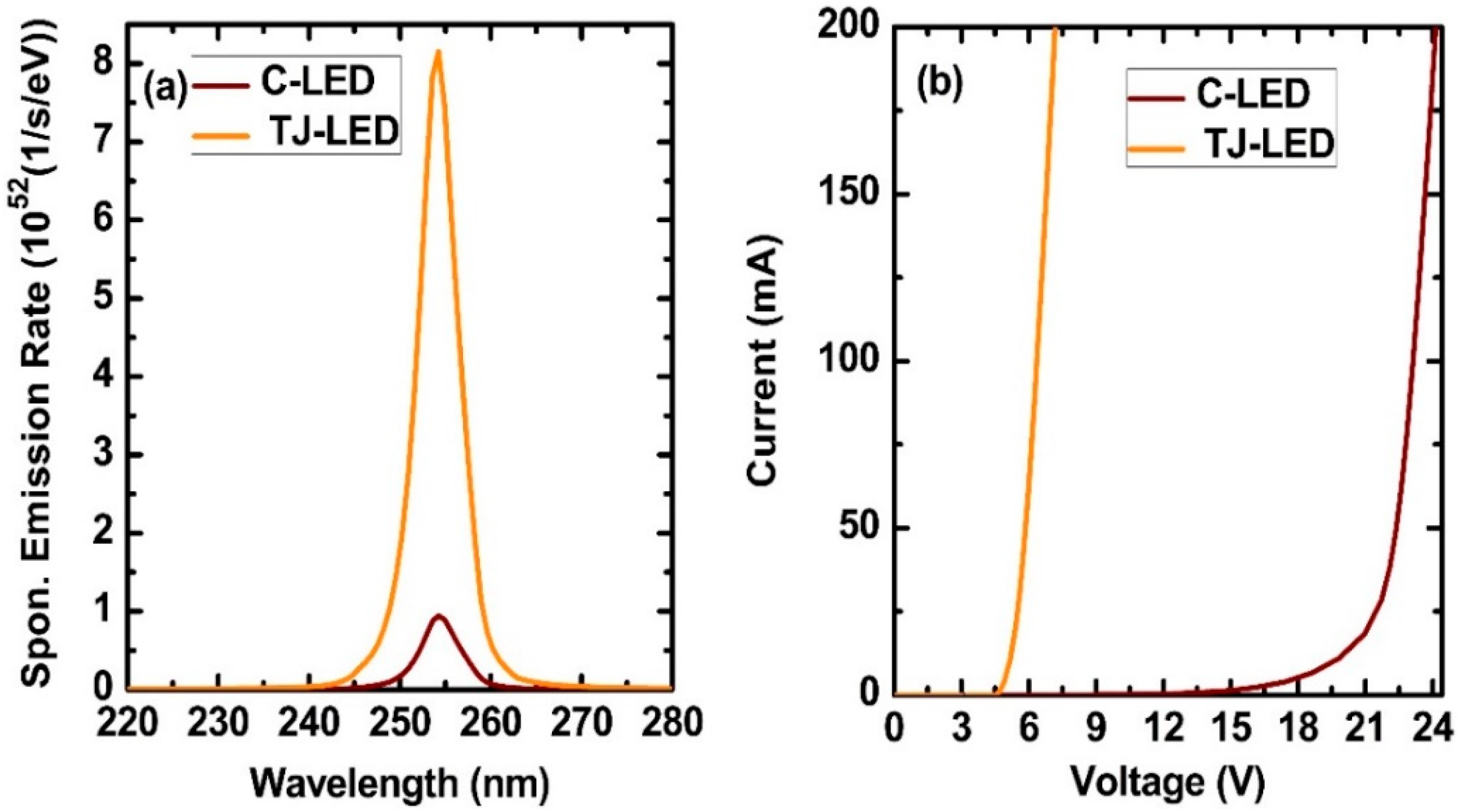
Figure 5a gives the emission spectra of C-LED and TJ-LED at the injection current of 200 mA, where the same emission peak wavelengths at 254 nm emission are successfully controlled. In addition, a much higher spontaneous emission rate was confirmed in TJ-LED which is approximately 8.5 times greater than spontaneous emission rate of C-LED. To further compare the electrical characteristics of both devices, we calculated the current-voltage (I-V) characteristics under injection current of 200 mA, shown in
Figure 5b and quite low operating voltages were observed in the TJ-LED, when compared to the C-LED. Previousley, our group reported about the experimental 254 nm DUV LEDs [
19], where donor–acceptor pair (DAP) emission was usefully suppressed but the operating voltage as high as 20 V on wafer was encountered [
19]. In this study, it was found that TJ-based LED possesses an overall improved device performance compared to the C-LED, including much reduced operating voltage from ~21 V to ~ 5.4 V at 200 mA, shown in
Figure 5b. Here it is worth noting that the band energy of C-LED is shifted to higher energy level as can be seen in
Figure 2a which is the main cause of high operating voltages. By introducing optimized TJ layer the depletion layer is replaced and conduction band/valence band alignment energies is shifted to lower energy level which help to reduce the the operating voltage in the AlGaN TJ-LED.
Figure 5.
(a) Spontaneous emission rate and (b) I-V characteristics of both LEDs.
Figure 5.
(a) Spontaneous emission rate and (b) I-V characteristics of both LEDs.
Moreover, it is concluded that this type of TJ (p-AlGaN/n-AlGaN) DUV LED has less resistance for current flow as derived from the slop of I-V curve, when compared to the C- LEDs, shown
Figure 5b. In case of TJ-LED the slop is quite linear and the turn on point is sharp thus offer a lower resistance. On the other hand C-LED turn on varies from 15 V to 21 V and the slop is higher compared to TJ-LED which attributes to higher series resistance in the C-LED.
Finally the IQE and light output power (LOP) of both the LEDs are compared and investigated in
Figure 6a,b. The significantly reduce auger recombination rate of TJ-LED lead to the IQE of 88% with zero efficiency droop, shown in
Figure 6a. The IQE (88%) of TJ-based LED is reported to be 1.3 times higher than the IQE (66%) of C-LED. Based on our known knowledge, 88% is the highest reported IQE at emission wavelength of 254 nm in the AlGaN TJ-based LED with efficiency droop of 0%, as shown in
Figure 6a. It was found that the LOP of the TJ-LED increases linearly with the varying current density, whereas the LOP of the C-LED increases nonlinearly first and then remain constant with the varying current density, shown in
Figure 6b. Contarory to the C-LED, it was can confirmed that the radiative recombination rate is linealy increases with the varying current density in the TJ-based LED. Such C-LED devices might enhances the thermal heating in addition to the junction temperature, whereas the TJ-LED might be safe from such unnecessary high thermal heating for package applications. TJ-based DUV LED devices can help in the higher WPE. The LOPs of 86 mW and 14 mW in the TJ-LED and C-LED, respectively, were achieved, shown in
Figure 6b. These findings are enlightened and convince the utilization of TJ in AlGaN DUV LED especially below 260 nm. Research and development of efficient AlGaN-based DUV LED at 254 nm emission wavelength is the safe and effective replacement of toxic mercury DUV lamp for the applciations in the unmanned enviroement to inactivate viruses and bacteria. Carrier confinement and transport issues in the MQWs of transparent DUV LED and micro-LED are quite critical for high performance devices [
2,
3,
12,
39,
40]. To resolve these issues of carrier confinement and transport, we provided a short roadmap for experimental efforts to realize high IQE beyond 88% in the TJ-based AlGaN DUV LEDs with impressive low operating voltage as well as with almost zero efficiency droop. The proposed TJ of DUV LED will open a better way for the realization of highly efficient UV LED panels for fast disinfection of surfaces, air, food, vegetables, and water in the unmanned environment.
Figure 6.
(a) Internal Quantum Efficiency (IQE) and (b) Light output power (LOP) of both LEDs under 200 mA current.
Figure 6.
(a) Internal Quantum Efficiency (IQE) and (b) Light output power (LOP) of both LEDs under 200 mA current.
