2. Materials and Methods
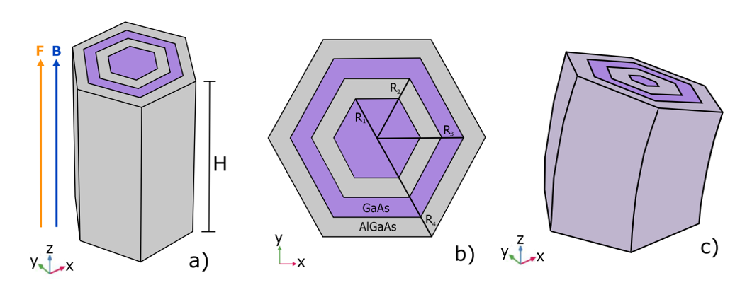
Figure 1(a) illustrates the structure of GaAs/AlGaAs hexagonal quantum wires without any revolution. The hexagonal arrangement consists of alternating GaAs semiconductor material (purple color in the first and third hexagon) and AlGaAs material (gray color in the second and fourth hexagon). The potential is set to zero within the GaAs material
, while in the AlGaAs material, it is represented by
. Additionally, a magnetic field
B and an electric field
F are applied in the
direction. These external fields play a crucial role in the confinement and manipulation of charge carriers within the quantum wire system.
To further investigate the properties of the system,
Figure 1(b) presents the hexagonal quantum wire at
, providing a clear visualization of the system’s geometry. The key parameters involved in the problem are indicated, including
,
,
, and
, which represent the radii of the four hexagons of the quantum wire. By specifying these parameters, we can precisely control the shape dimensions and geometry of the quantum wire structure, which in turn influences the electronic and optical properties under investigation.
To explore the effects of rotation on the quantum wire system,
Figure 1(c) showcases the hexagonal quantum wire after rotation. A rotational transformation is applied with a radius of revolution,
, and an angle of rotation,
. This rotational operation introduces a modified curvature to the wire while preserving the arc length. The introduction of an adimensional factor,
the revolve parameter, allows us to adjust the curvature while maintaining the desired wire length along the
direction. The relationships governing this modified curvature are expressed as
,
. It does not make sense to express the height of the quantum thread along
z with
H, but rather the product
. This rotational transformation enables the study of the influence of wire curvature on the electronic and optical properties of the system.
To numerically investigate the GaAs/AlGaAs hexagonal quantum wire system, we employ the powerful computational tool, Comsol Multiphysics. Specifically, we utilize the software’s Revolve functionality, which integrates the FEM to accurately solve the governing equations. The Revolve functionality is well-suited for modeling rotational symmetry in the system, allowing for a comprehensive analysis of the quantum wire’s properties.
In our simulation setup, Dirichlet boundary conditions are imposed on the sides of the last AlGaAs hexagon (with ), as well as on the front and rear covers of the system. These boundary conditions provide a physically realistic representation of the wire system and ensure accurate calculations of the electronic states and optical properties.
The electronic structure and optical properties of the system are elucidated by solving the Hamiltonian governing the quantum wire. The Hamiltonian is expressed as:
where is the electron effective mass, is the static dielectric constant (the index w, b indicates the core or shell materials respectively). Within this Hamiltonian, the confinement potential is defined as for GaAs quantum wire wells and for AlGaAs quantum wires barriers. The first term in the Hamiltonian accounts for the kinetic energy of the charge carriers, including the momentum and the vector potential of the magnetic field . Besides, represents the potential vector associated to the applied magnetic field, where comes from the gauge. The second term represents the confinement potential, which differs between GaAs and AlGaAs regions. The third term accounts for the interaction of the electric field with the charge carriers, where e represents the charge of the electron and F denotes the magnitude of the electric field in the direction. The final term in the Hamiltonian captures the Coulomb interaction between charges, with e representing the impurity charge and r denoting the distance between electron-impurity, with the impurity at a fixed point . Here, is a parameter that controls the presence or absence of the shallow donor impurity ( = 0 removes the impurity effects whereas = 1 turns them on).
To accurately describe the electronic and optical properties of the system, it is essential to consider the effective masses of the charge carriers. In our study, we utilize an effective mass of for GaAs and for AlGaAs. These effective masses account for the differences in carrier behavior between the two materials.
At the interface between GaAs and AlGaAs, the boundary conditions follow the approach established by Ben-Daniel and Duke [
33,
34]. These boundary conditions ensure a smooth transition of the electronic states across the material interface and provide a realistic representation of the heterostructure.
By solving the Hamiltonian using the FEM-based Comsol Multiphysics software, we obtain the electron states and corresponding wave functions for the system. These electron states are then utilized to evaluate the optical properties, particularly the transitions from the ground state to excited states.
Furthermore, we analyze the nonlinear optical absorption coefficients, following the framework proposed by Ahn and Chuang [
35,
36]. These coefficients, denoted as
, capture the intensity of the absorption process at different frequencies. They depend on various factors such as the incident photon frequency
, the electron density
, and the matrix elements of the dipole moment
. The damping term,
, is inversely related to the relaxation time
of the excited states.
In our calculations, we account for fundamental physical constants such as the permeability of free space (
), the vacuum permittivity (
), and the speed of light (
c). The relative permittivity of the material,
, characterizes the dielectric properties of the quantum wire system. The elements of the dipole matrix moment for light polarized along the
direction are calculated using the following:
The calculated matrix elements provide insights into the strength and nature of the optical transitions occurring within the quantum wire system.
Finally, we emphasize that this study focuses on exploring the electron confinement effects related to the dimensions of quantum wires and the impact of externally applied electric and magnetic fields. Additionally, we investigate the influence of shallow donor impurity effects on the semiconductor nanostructure properties.
3. Results and Discussion
To further investigate the properties of the system, the key parameters involved in the problem are indicated, including
nm for the GaAs core,
nm (AlGaAs shell),
nm (GaAs shell) and
nm (AlGaAs shell), which represent the radii of the four hexagons in the quantum wire, see
Figure 1 presents the hexagonal quantum wire base at
plane, providing a clear visualization of the semiconductor nanostructure geometry.
nm and revolve effect parameter
fixed and
rad. The setup for the potential energy and effective mass are
and
for GaAs and
meV and
for AlGaAs, where
corresponds to the mass of a free electron. In our calculations, we account for the relative permittivity value
, the nonlinear optical absorption coefficients for light polarized along the
direction are calculated using the following: The damping term,
ps, is inversely related to the relaxation time
of the excited states and density
m
. The other variables are the fundamental physical constants such as the permeability of free space
, the vacuum permittivity
,
e represents the charge of the electron and the speed of light
c.
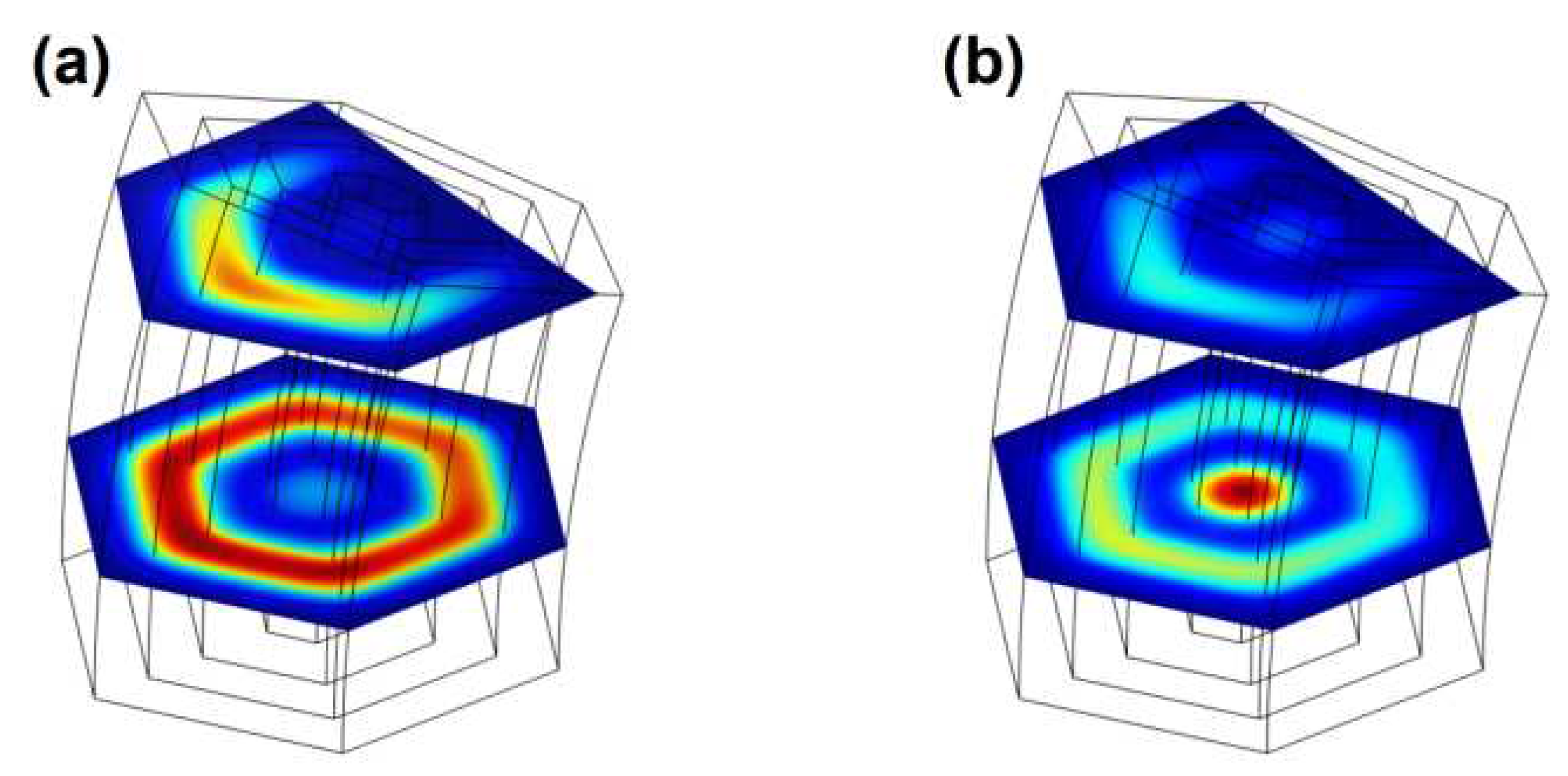
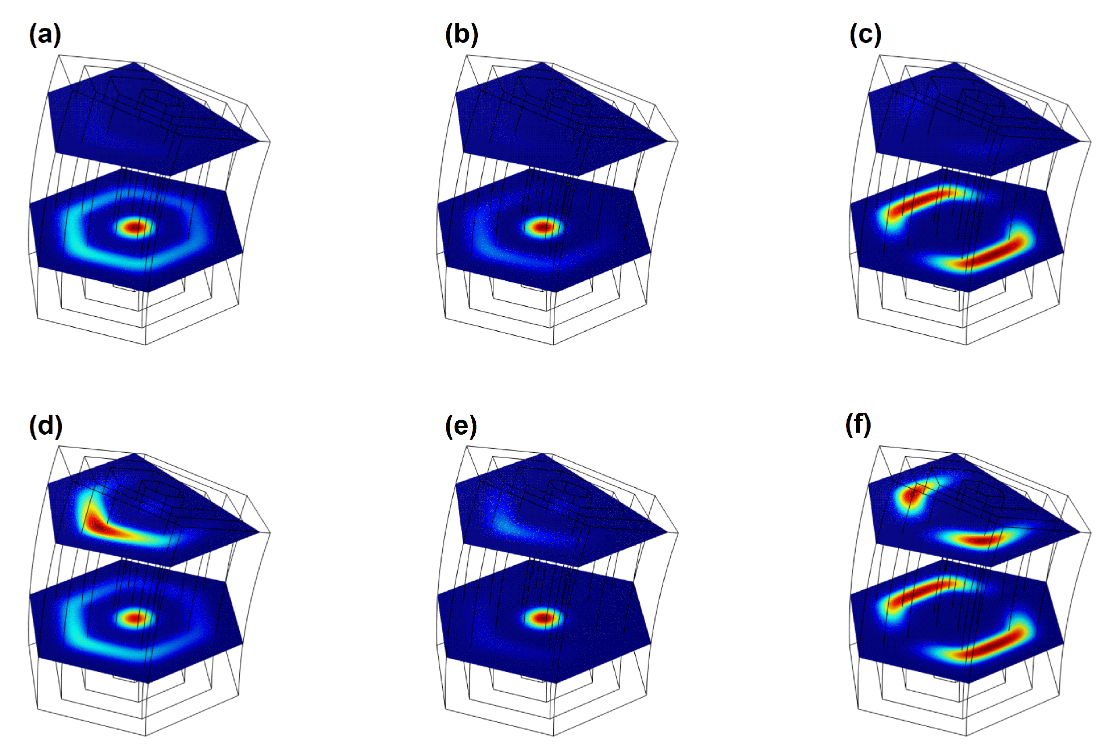
A pictorial view of the electron ground state wave function projections corresponds to the intersection of the hexagonal GaAs/AlGaAs quantum wire and a revolve effect, with the planes at
nm, the lower one at
nm, shown in
Figure 2, without electric and magnetic fields effects.
In
Figure 2(a) the wave function correspond to the case without donor impurity, it is observed that the wave function mostly spreads in the region of the GaAs shell with radius
, this means that the electron is confined between the AlGaAs shells that forms a region of hexagonal barriers. It is observed that the highest probability of finding this with an intense red color in the plane
nm and in yellow color a lower probability is observed in the
nm plane, in these case the wave function only occupies a V-type region.
When we place a donor impurity at
nm, the electron is most likely confined to the GaAs nucleus with radius
, the intense red color region (a virtual quantum dot) to the bottom of the quantum wire (at
nm) appear, see
Figure 2(b). Some probability minor is seen in the hexagonal region between
and
that cut
nm, these very low probability of the localize the electron are in the region in V-type form weakly painted in white color is observed, from here we can say that the presence of the impurity confines the electron in the lower region of the quantum wire close to the base in
.
In
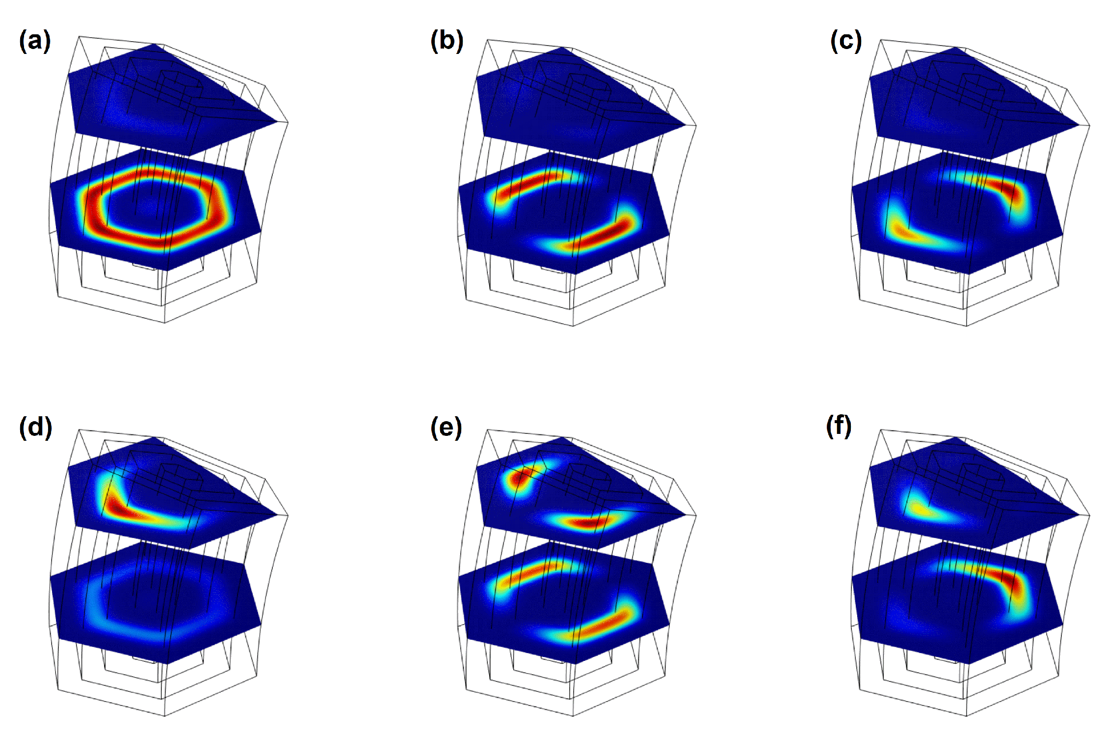
Figure 3 we present the wave function of the ground state and the first two excited states of an electron confined in a quantum wire without impurity.
Figure 3 (a, b, c) show the effect of an electric field of
kV/cm, applied parallel to the positive
axis and
Figure 3 (d, e, f)
kV/cm, that is, applied anti-parallel to the positive
axis.
Figure 3 (a, b, c) confirm the fact that a positive electric field repels the electron confining it towards the region of the base of the quantum wire, this is observed by the maximum probabilities (in red color) in the plane
nm and practically zero probability in the plane
nm (in blue color). In
Figure 3(a) we have the fundamental state
, in
Figure 3(b) the first excited
and in
Figure 3(c) the second excited
, regarding the excited states it can be see that its probability is "rotated by 90°", this is because all wave functions (and their projections) are orthogonal and normalized, this behavior explains why in
Figure 4(a) the energy curves
and
are degenerate in the range from
kV/cm to
kV/cm, keeping the electron confined in this region.
Figure 3(d, e, f) illustrates the electron wave functions for an electric field of
kV/cm, corresponds to first, second and third states, respectively. In
Figure 3(d) the clear effect on the charge location probability within the system is evident. When the electric field is applied in the direction opposite to the
axis, we can see the formation of a virtual V-groove quantum dot (intense red color) becomes apparent in plane
nm, while in
nm a slight probability appears, with a tendency to zero, in white color, these phenomenon influenced by the unique asymmetry that revolve parameter induces. On the other hand, in
Figure 3(e, f) exhibits this same effect but with the activation the wave function in both cuts, distributing the probabilities of locating the electron in some regions in the hexagons, it is important to note that the differences with the wave functions shown in
Figure 3(b, c), explain why in this case the states
and
are not degenerate in the entire range between -50 kv/cm and 0 in
Figure 4(a).
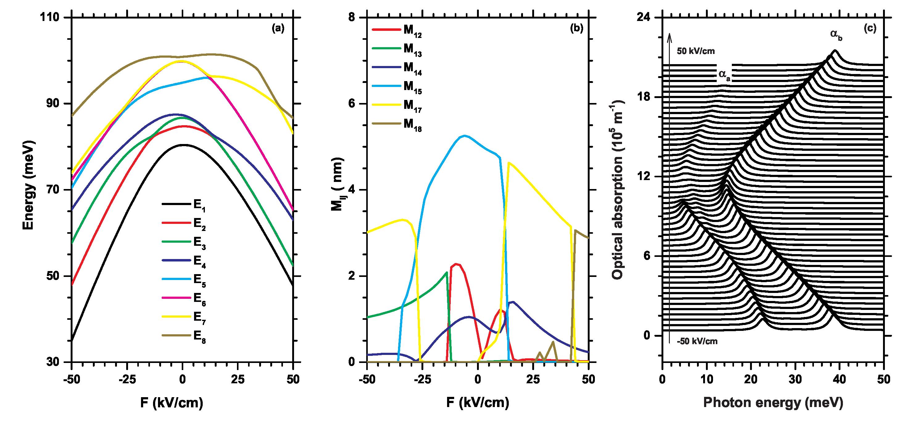
In
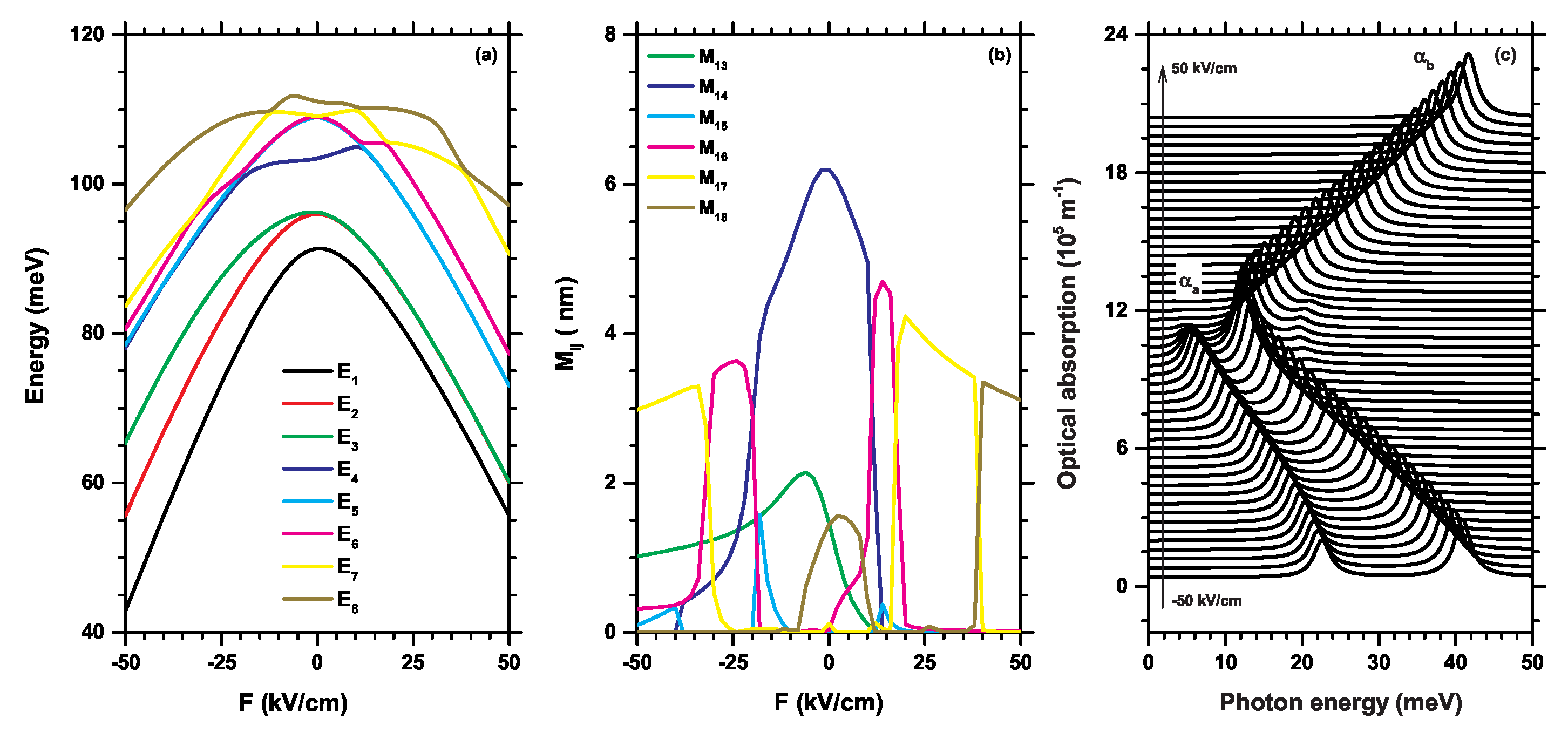
Figure 4 are shown (a) the electron energies, (b) dipole elements and (c) absorption coefficients as a function of the electric field strength
F, without donor impurity (
) in hexagonal GaAs/AlGaAs quantum wires. In this case we have fixed the geometrical dimensions of the quantum wire:
nm,
nm,
nm, and
nm which represent the radii of the four hexagons of the quantum wire and
nm,
rad and
.
In the
Figure 4(a) depicts the energies corresponding to the lowest energy states of the electron confined within a multi-layered quantum wire, as a function of an external electric field applied along the
axis. The magnitude of this field varies from -50 kV/cm to zero, for anti-parallel to
axis and from zero to
kV/cm in direction parallel to
axis. Given the asymmetry introduced by the revolve factor
, these electron energies curves are also asymmetric. This asymmetry can be observed, for instance, in the ground state, where the electron’s energy approximates
meV at
kV/cm and approximates
meV at
kV/cm. The same asymmetric behavior applies to for all excited states. We observe the special effect of the geometrical asymmetric in combination whit the electric field over the first and second excited states, in the regimen of the anti-parallel direction these energies are separated for a 10 meV of difference, but in the parallel direction, after the electric field strength in zero values these energies are degenerates until
kV/cm. For fourth, fifth and sixth excited states, the energies curves present anti-crossing phenomena between their in several points correspond with the both parallel and anti-parallel regime, can see at round to 0, 10 kV/cm, 20 kV/cm and 40 kV/cm. The energies that correspond to seventh and eighth states only have tree point with anti-crossing and both curves are totally asymmetric. In a hypothetical scenario where the hexagonal quantum wire was upright, meaning that the axis of the quantum wire would align with the
axis, the energy curves presented would be symmetric and degenerated in accordance with the symmetry delineated in
Figure 1(a). When the electric field is applied in the same direction as the
axis, i.e., in the range of 0 to
kV/cm, the electron, repelled by the electric field, demonstrates a probability to localize its wave function in the lower region of the quantum wire. This area represents the region of maximum geometric confinement, caused by the parameter
.
For the third excited state (
), in
Figure 4(a), there is an inflection point at approximately
kV/cm, while in Figure 6(a), this same state presents a maximum, and the same behavior of changing critical points occurs in states
and
. At the same time, when the impurity is not present,
is degenerate to
, except between
kV/cm and
kV/cm, where they are not. Conversely, when there is the presence of impurity,
is always degenerate to
, and even between
kV/cm and
kV/cm,
and
are degenerate. Another interesting detail is that, given the crossings between the first and second excited state at approximately
kV/cm and
kV/cm, they favor the emergence of a transition probability between the ground state and the first excited state that previously did not exist in
Figure 4(a).
The elements of the dipole matrix
depending on the magnitude of the electric field are presented in
Figure 4(b), this allows to study the transitions allowed between the ground state and the corresponding excited states for which this occurs. Linear polarization along the
axis has been considered to analyze the relationship with the electric field in both regimes.A non-uniform oscillatory behavior can be observed in the curves of the dipole elements, this behavior is associated with the crossings that have the states with energies
to
as can be seen in
Figure 4(a). The dipole element
has positive values from
kV/cm and then drops to zero at
kV/cm.
is different from zero in the range from -19 kV/cm to 16 kV/cm, and is also the largest magnitude,
it only has a few points where it is different from zero, at: -40 kV/cm, -20 kV/cm and 13 kV/cm, which he understands by
to be a state that is degenerate with
for values greater than
kV/cm. The ranges where
is different from zero are from -33 kV/cm to -20 kV/cm and then between 17 kV/cm to 19 kV/cm,
between -50 kV/cm to -35 kV/cm and from 20 kV/cm to 37 kV/cm, finally
is only different from zero between 40 kV/cm to 50 kV/cm. The crossings observed in the energy curves in
Figure 4(a) cause, for example, that the positive values of the dipole elements from
to
to form a "curve" of positive values, making it possible to add the respective values of the absorption coefficients
to
.
In
Figure 4(c), the transition energy effects (
) over the optical absorption coefficients,
and
, can be observed. The amplitude of these absorption coefficients is proportional to the product of the squared dipole moment and the transition energy, i.e.
. For
, represented by
plus
, a redshift is noticeable as the field becomes smaller for negative values of
F, between 22.70 meV at -50 kV/cm and 5.70 meV at 12 kV/cm, respectively, after this electric field value the dipole
becomes zero, therefore there are no absorption coefficient peaks. For
, represented the sum of
,
,
, and
, the behavior demonstrates a redshift while under a negative electric field, from 40 meV at -50 kV/cm to 14 meV at 0 kV/cm, where is also the maximum amplitude of all the peaks of the optical absorption coefficients presented here and a blueshift when the electric field carries positive values, from the value corresponding to zero of the electric field to 41.50 meV at 50 kV/cm. The locations of the peaks of the optical absorption coefficients are in the range of allowed energy transitions, which correspond to the far infrared, between 1.38 THz and 10 THz, that is, to a semiconductor nanostructure such as this quantum wire with revolve effect, its optical response can be modulated with effects of electric fields, such as are presented in this work.
In
Figure 5, they are presented in the same geometric conditions and applied electric field values as in
Figure 3, the fundamental difference is that a donor impurity is placed at the point
nm. As can be seen in the figures (a, b, c), the presence of the donor impurity repels the electron and the effect of the electric field of
kV/cm is reinforced, confining the electron near the cutting plane at
nm. In the ground state (a) and first excited (b) the combined effects of impurity and electric field locate the electronic probability in the central hexagon (or core), in a virtual quantum dot, the second is excited (c), it is located in the same plane, but rotated 90° with respect to the
Figure 3(c), an effect that is essentially due to impurity. In this case it can be seen that the electron wave functions, although they are orthonormal, correspond to values where the associated energies are not degenerate, precisely because of the notorious differences between (b) and (c), (e) and (f). It is also important to clarify that at small values of the electric field (positive or negative) or in a weak regime, the presence of the impurity dominates the location of the electronic probability in the hexagonal core (
of GaAs, while for the strong regime of the electric field (for example
kV/cm), the effect of the field is dominant over that of the impurity.
In
Figure 6, the same panels as in
Figure 4 are presented, but in this case, within the hexagonal quantum wire system, there is a donor impurity at a height in the
nm. Thus, for
Figure 6(a), the first noticeable effect of the donor impurity is that the energies of both the ground state and the excited state decrease by approximately 9 meV (see the vertical axis in
Figure 6 vs.
Figure 4), due to the confinement the impurity grants to the electron. Another interesting effect that can be observed is that while in
Figure 4(a), the first and second excited states (
and
respectively) are degenerate for positive values of the electric field, in the case of
Figure 6(a), these are barely degenerate for values greater than approximately 12 kV/cm.
Figure 6(b) shows the elements of the dipole matrix with the same configuration as
Figure 4(b), considering the presence of impurity (
), oscillations in the curves of these dipoles are also observed, the three main facts being: The values of all the dipoles drop by almost 1 nm on average, the second is that the
dipole appears with a non-zero value between -15 kV/cm and 15 kV/cm and the third news is that a change occurs between the
and
dipole curves (compared to those of
Figure 4(b)). This causes the appearance of a permitted transition formed by the dipoles
,
and
. This behavior is responsible for the appearance of peaks in the optical absorption coefficients up to 40 kV/cm, a fact that does not occur when the impurity is off (
), this due to the location of the electronic probability by the impurity along the
z-axis.
In
Figure 6(c), we can study the optical absorption coefficients
and
associated with the changes in transition energy for due to the presence of a donor impurity. If this graph is compared with
Figure 4(c), though the amplitude of these in
Figure 6(c) is less prominent than that shown in
Figure 4(c). In
, for positive electric field values, there exists a small peak not found in
Figure 4(c). This is attributed to the probability of a transition between the ground state and the third excited state (
), which did not exist previously in the absence of impurity, this is
in figures presents a redshift for negative electric field values, from 23 meV at -50 kV/cm to 4.10 meV at zero and a blueshift for positive values, from 23 meV at -50 kV/cm to 13.10 meV at 40 kV/cm, from this value to 50 kV/cm the dipoles become zero, that is, energy transitions are not allowed in that range of electric field values between the first three excited states and the ground state, respectively. However, the path followed by the optical absorption coefficient
in
Figure 6(c) is 3 meV less compared to its counterpart in
Figure 4(c), this can be attributed to the impurity which, as observed in
Figure 6(a), causes lower energy values; also note that there is a redshift for negative values of the electric field and a blueshift for positive values.
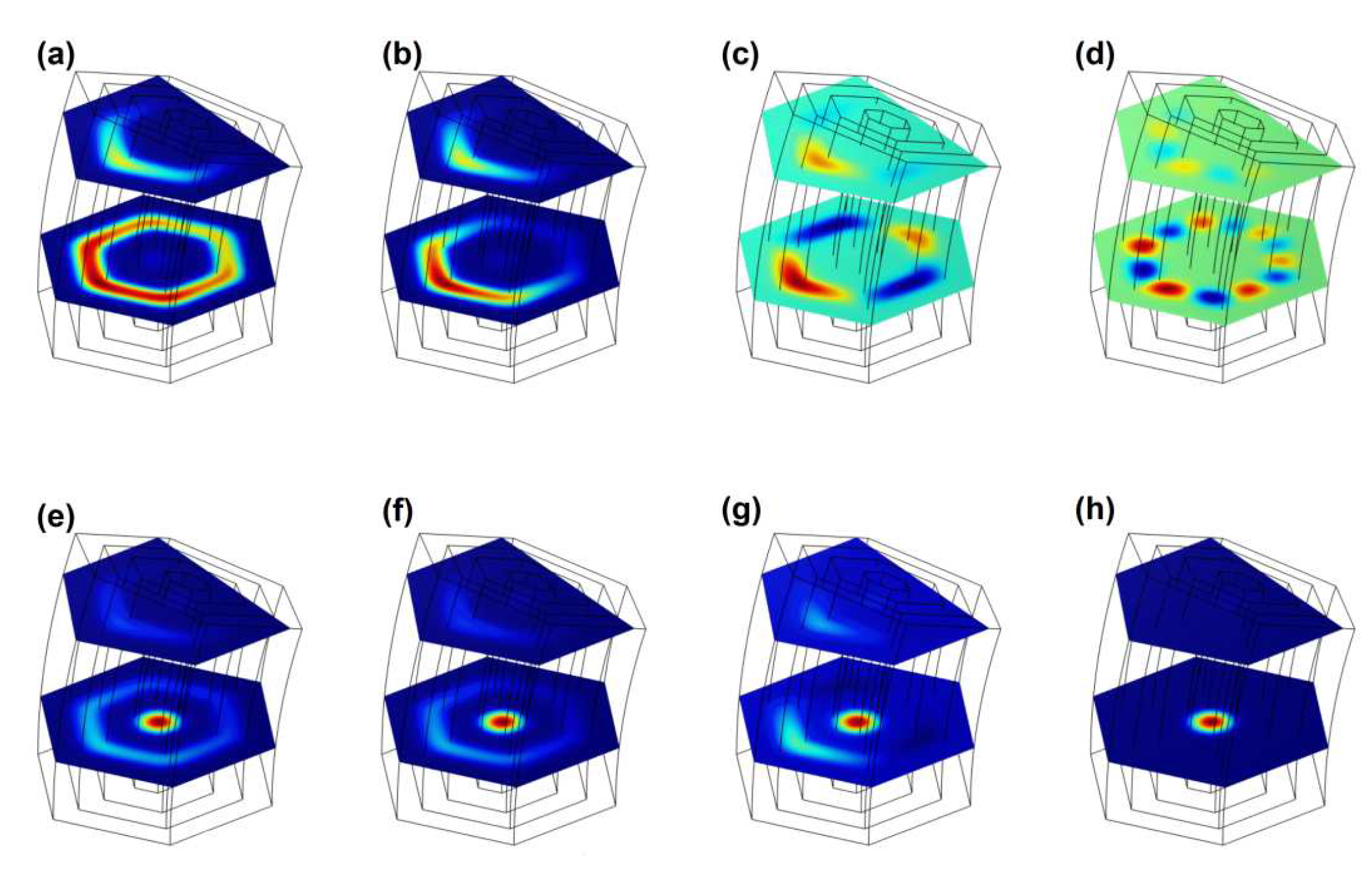
Figure 7 show the wave function of the ground state of the electron. Upper panel (a, b, c, d) without donor impurity, lower panel (e, f, g, h) with donor impurity (at
nm). The effects of the external magnetic field are shown in the following order: At (a, e)
T, at (b, f)
T, at (c, g)
T and in (d, h)
T, in GaAs/AlGaAs hexagonal quantum wires with revolution parameter
and the fixed geometry related in this work. The magnetic field is applied in the positive direction of the
axis.
In the
Figure 7 of the upper panel without impurity (
), three fundamental effects are noted, the first that the increase in the magnetic field
B from 1 T, to 5T, 10 T and finally 30 T, leads to the location of the wave function of the electron to be confined in a virtual quantum ring for the weak regime of B in the region of the hexagon of radius
(the third shell), until forming coupled points, this in the cut of the plane at
nm, with the quantum thread. The second is that when the value of
B increases, the probability of locating the electron in the
nm plane becomes lower, the third effect is that this type of confinement evolution causes the energy of the ground state to increase and have smooth oscillations, see
Figure 8(a), black curve (
).
In the case of the lower panel, where there is the active donor impurity (
), it is noted that by increasing the
B value, the electron wave function is very well located in the cut of the hexagon of radius
(core), of the quantum wire, with the plane at
nm, that is, the magnetic field confines the electron in a virtual quantum dot, combined with the presence of the donor impurity that rejects the electron towards that lower region of the nanostructure. It is clearly seen that the probability of locating the electron in the
nm plane becomes zero as
B increases .Another quite noticeable effect of the combination of a magnetic field and the presence of the donor impurity is that the oscillations of the ground state, black curve
, and the first excited state, red curve
, tend to disappear,see
Figure 9(a).
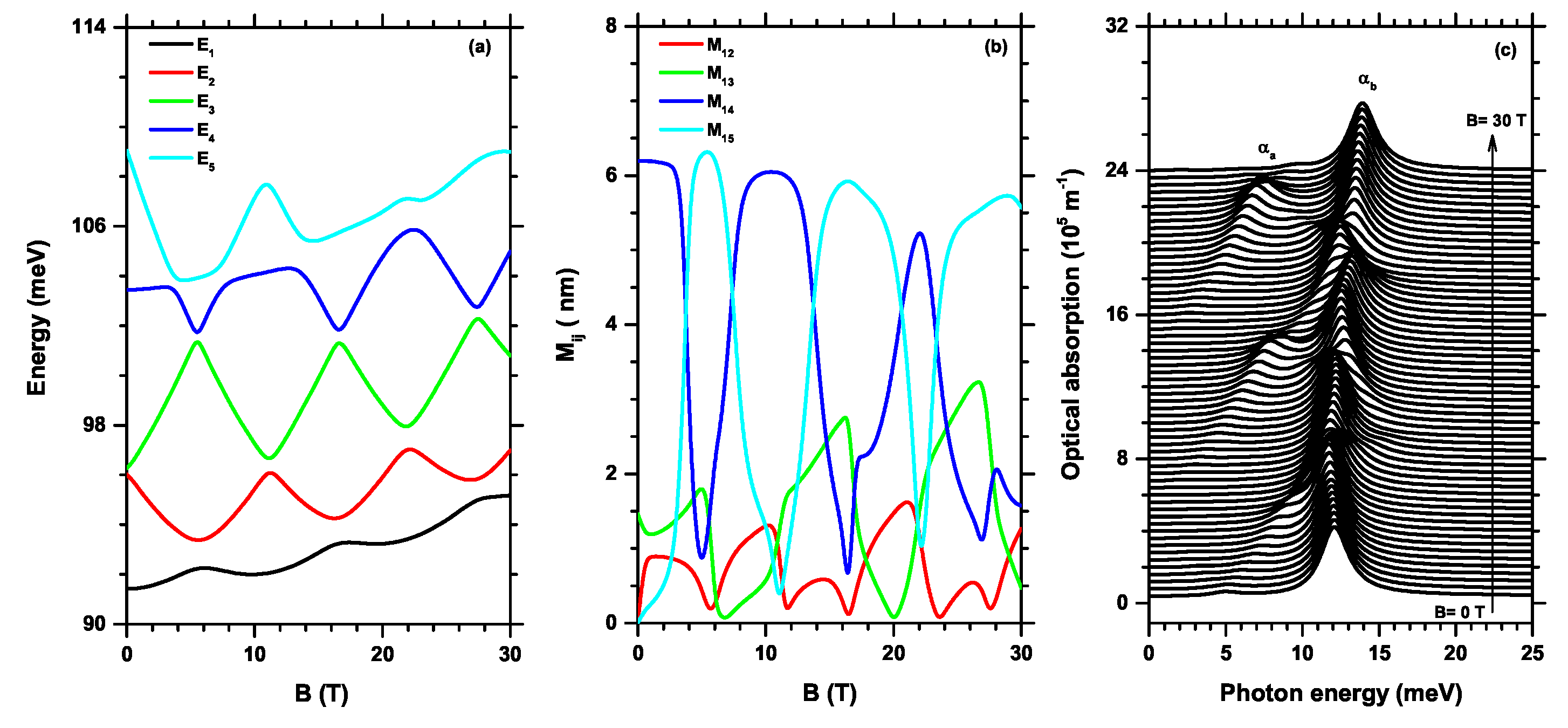
In
Figure 8, the effect of the magnetic field is analyzed for (a) electron energies, (b) dipole elements and (c) optical absorption coefficients. Particularly in
Figure 8(a), the energy levels of an electron confined within a hexagonal quantum wire, under the influence of a magnetic field applied in the
z direction, are displayed. The magnitude of this field varies from 0 to
T. The energy range of the first five states is between 92 meV and 109 meV, much smaller than the range due to the electric field. The figure clearly depicts the oscillations induced by the magnetic field in the energies of the excited states, and to a lesser extent, in the ground state. Concurrently, it becomes apparent that as the field intensity increases, the energy levels increase. for
, it can be observed that the energies of the first two excited states are degenerate, the only time it occurs in the first five states shown here. However, this degeneracy was broken when a magnetic field was applied and multiple crossovers occurred between all energy levels for particular magnetic field values, causing accidental degeneracies. This resulted in an oscillating pattern of energies as a function of B, and at the crossing points, the wave functions are swapped at those points correspondingly.
Figure 8(b) shows the oscillating behavior of the elements of the dipole matrix as a function of the magnetic field, the ones with the greatest amplitude being those of the elements
(blue color curve) and
(cyan color curve), the maximum values of these dipoles alternate around 5 nm and 6 nm. Another group of dipoles is formed by
(red color curve) and
(green color curve), their maximum amplitude range is between 2 nm and 3 nm, respectively, throughout the
B scan. These dipoles are associated with transitions with a non-zero probability of occurring when a magnetic field is applied.
Figure 8(c) shows two groups of nonlinear optical absorption coefficients (
and
) depending on the energy of the incident photons for different values of the magnetic field between 0 and 30 T, associated with the differences between the energies
shown in the curves of
Figure 8(a) and the squares of the dipole elements
in
Figure 8(b). For the coefficients grouped in
it is observed that the optical absorption peaks oscillate as do the energies and the dipoles, these coefficients present a shift towards the blue in general, but their amplitudes are smaller because they come from the dipole elements
and
, the lowest value peak, which coincides with the energy of the photons at
meV which corresponds to 1 THz. The coefficients
are mainly located at 12 meV for
and 14 meV at
T, with small oscillations that vary according to the transition energies
and
multiplied with the squares of the
and and
dipoles, correspondingly, these coefficients have their peaks almost centrally aligned. For these optical responses the frequencies are oscillating around 3.36 THz, in the far infrared.
Finally,
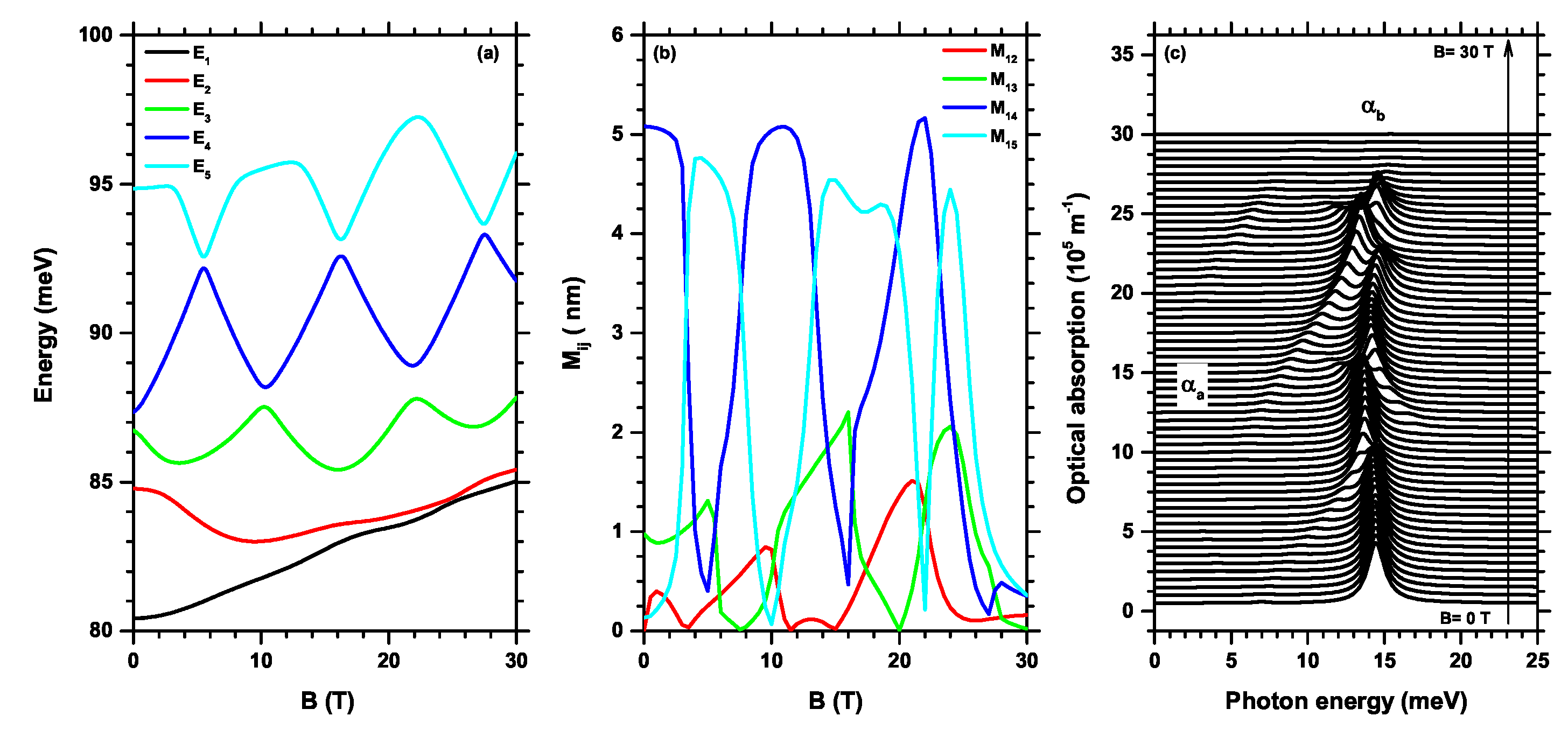
Figure 9 shows the combined effects of a magnetic field with the presence of a donor impurity in the semiconductor nanostructure of a core/shell/shell type quantum wire, on the energies of the first five electronic states (a), the elements of the dipole matrix (b) and the optical absorption coefficients (c) associated with the allowed transitions. The configurations of the geometry and the values of the magnetic field are the same as those considered in
Figure 8 and the active impurity in at
nm. In
Figure 9(a), the energy curves of the first five states generally lower their value, compared to those presented in
Figure 8(a), this can be seen in all extreme values of the magnetic field, in general, the range of energies is between 80.50 meV at
for the ground state (
) and 97.50 meV at
T for the fourth excited state (
). In this energies range, the energy transitions occur if the corresponding dipole is different from zero. On the other hand, the effect of the magnetic field combined with the donor impurity, causes the electron to be confined in the
region, which is the core of the structure, causing the curves of both the ground state and the first excited state to "smooth", losing the typical oscillations caused by the magnetic field only. The other three excited states keep this characteristic behavior, favoring the typical crossings for some specific values of the magnetic field.
The dipole elements are presented in
Figure 9(b), it is observed that the group of elements
and
also present the oscillatory behavior and their maximums are between 4 and 5 nm, that is, they have dropped almost 1 nm, if compare with those of
Figure 8(b). for the group
and
, which have their maximums between 1 nm and 2 nm, there is also an equal decrease, 1 nm, in their magnitude, an effect due to the presence of the donor impurity, it is also noteworthy that all the dipoles fall towards zero, after
T, a fact that converts the optical absorption coefficients to zero between 24 T and 30 T, as can be seen in
Figure 9(c).
The optical absorption coefficients presented in
Figure 9(c), are associated with the energy transitions and the corresponding dipole elements, thus in
with the
proportional to
added with the
which are proportional to
, equal for
. The optical absorption coefficients
present their peaks oscillating around a central value of 14 meV, with small shifts towards the blue, which do not exceed 15 meV, very similar to the previous case with a magnetic field, but without impurity, however, in this case, with donor impurity present, the coefficients disappear after 24 T and the peaks appear more aligned, obviously of greater amplitude than those of the coefficients labeled
. With a small amplitude and with a blue shift. the coefficients
are observed, their peaks are located in corresponding regions of photon energy between 1.24 meV and 9.30 meV close to 28.50 T. These energy ranges correspond to photon frequencies between 0.36 and 3.38 THz.
