1. Introduction
Nowadays, in many applications, the market pushes towards the concurrent reduction of the bill of materials and the increment of power density [
1,
2]. The first target is achieved by adopting mature technologies with a good tradeoff between investment and performance [
3]. The latter target can be obtained by operating the power converter at a high switching frequency to reduce the size of the passive components, thus also benefiting from the cost reduction [
4]. However, an increment in the switching frequency inflicts increased switching losses that can considerably compromise power efficiency [
5]. Furthermore, high-density high-frequency power converters lead to challenging thermal issues management [
6]. This task becomes harder when the power converter is frequently operated at high/full load [
7]. The thermal operating conditions of the power devices critically affect their lifetime [
8].
Considering all the aforesaid aspects, a cost-effective solution can be reached using power devices able to ensure good efficiency when operated at high frequency and high load. SuperJunction (SJ) MOSFETs enhanced by the introduction of an additional source pin, called Kelvin source, is the best compromise solution [
9]. At high loads, these devices presenting 4-lead (4L MOSFETs) strongly reduce the switching losses and, consequently, the device and converter operating temperature in comparison with 3-lead MOSFETs [
10]. However, it is necessary to fully understand the reasons behind this improvement to fully exploits the advantages of 4L MOSFETs.
This paper investigates the improvement mechanisms involving a reduction of the switching losses during the turn-off [
11]. Firstly, a comparison of the switching losses is presented. After that, the switching waveforms are analyzed to properly model the devices during the interval in which the greatest part of the turn-off losses occurs. Then, the circuit model is analyzed and an approximate analytical expression of the current slew rate is obtained for both kinds of devices packaging. The comparison of these equations has highlighted that the turn-off improvement obtained by adopting the Kelvin source is due to the lower inductance of the driver loop in comparison with the power loop inductance
2. Comparison of the experimental turn-off losses
A boost converter has been selected for analyzing the turn-off behaviour of 3L and 4L MOSFETs. The device is a TO-247-packaged N-channel MOSFET:
- −
breakdown voltage 650V;
- −
on-state resistance 37 mΩ;
- −
maximum current 58 A.
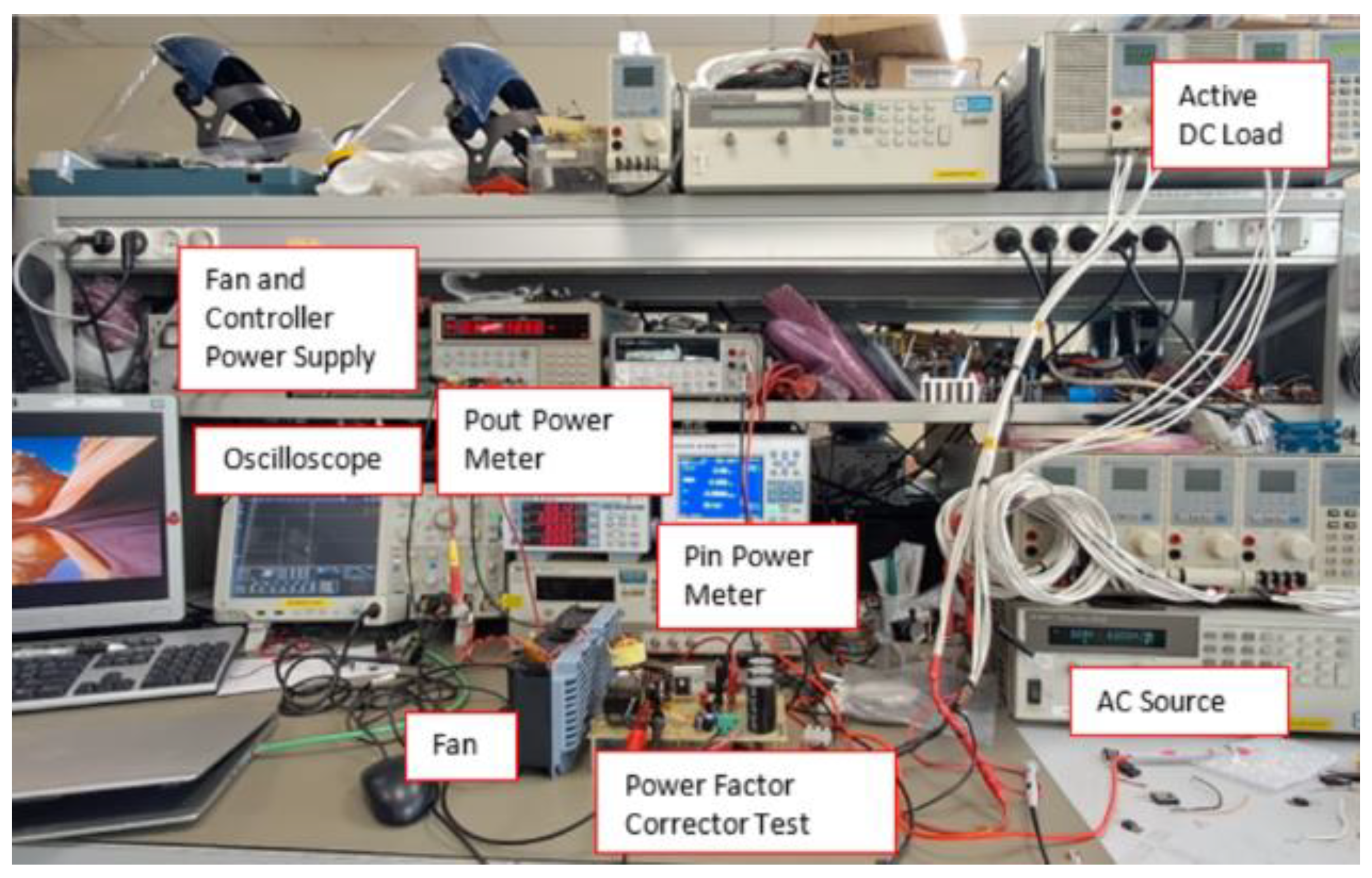
The test vehicle is the boost converter reported in
Figure 1 with the overall experimental setup.
The test equipment consists of the following components.
- −
AC source: Agilent AC/DC power supply 6813B (1750VA).
- −
Oscilloscope: 1GHz Tektronix MS05140.
- −
Yokogawa power meter WT500 and WT310 to measure, respectively, the input and output power.
- −
Chroma DC Electronic Load Model 6314 to set the output current (active load).
- −
Tektronix current probe TCP0030 to measure the MOSFET current.
- −
Tektronix passive voltage probe (1:10) to measure the gate-source voltage.
- −
LeCroy passive voltage probe P6139B (1:100) to measure the drain-source voltage.
Finally, an auxiliary power supply has been used to supply the cooling fan.
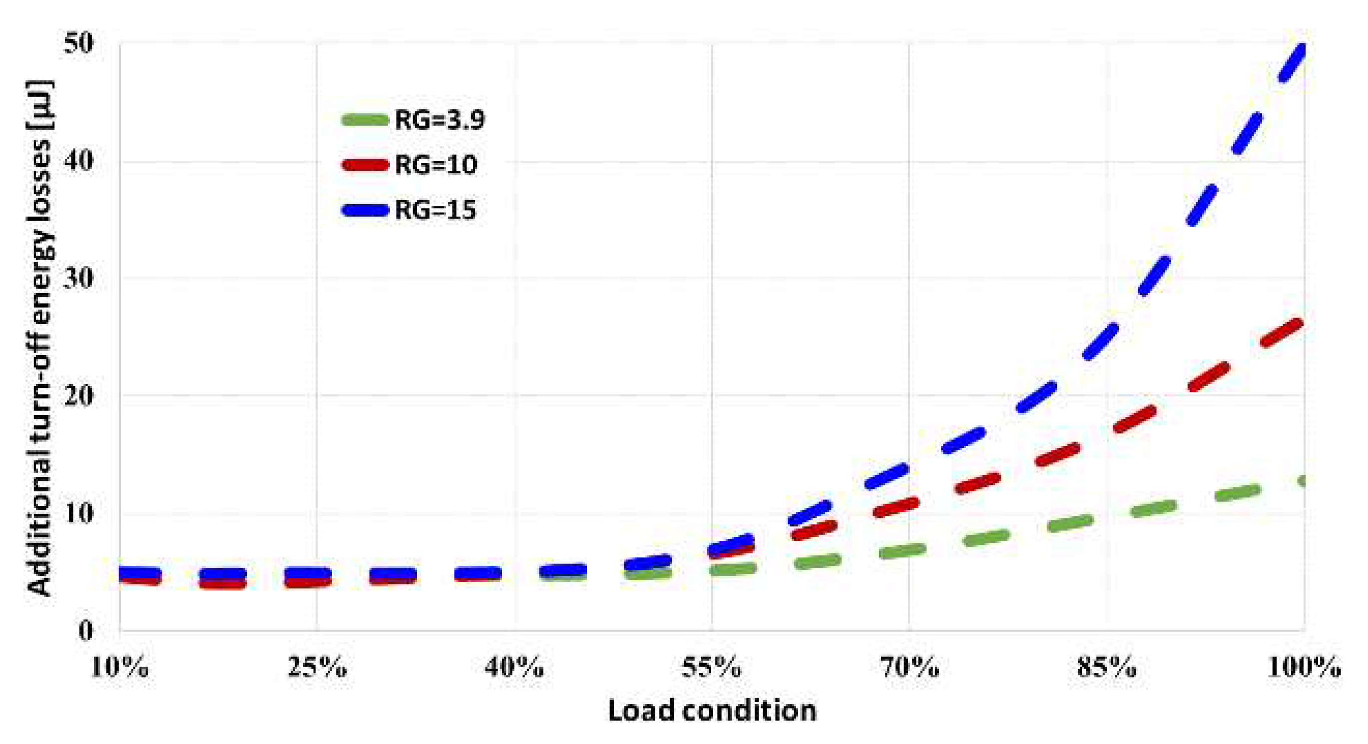
Figure 2 reports the variation of the difference between the turn-off energy losses of 3L and 4L MOSFETs as a function of the converter load. In other words, the figure reports the additional switching losses due to the use of a 3L MOSFET instead of the same device enhanced by the Kelvin source.
The results are reported for a typical RG (3.9Ω) and greater values of the gate resistance. It is interesting to note that curves overlap for low load levels (<45%), this means that there is a negligible effect of the gate resistance. Moreover, also the load level has not any effect, as highlighted by the constant additional losses. For a load level greater than 45%, the curve does not overlap more. Consequently, the additional losses depend on the gate resistance: they increase as the resistance increases. Considering that the gate resistance regulates the switching speed that, in turn, affects the switching losses, the increment of the gate resistance slows more the 3L MOSFET turn-off than the 4L one.
In this load range, also the load itself affects the additional energy losses because they increase as the load increases. Therefore, also the load current differently affects the turn-off switching speed.
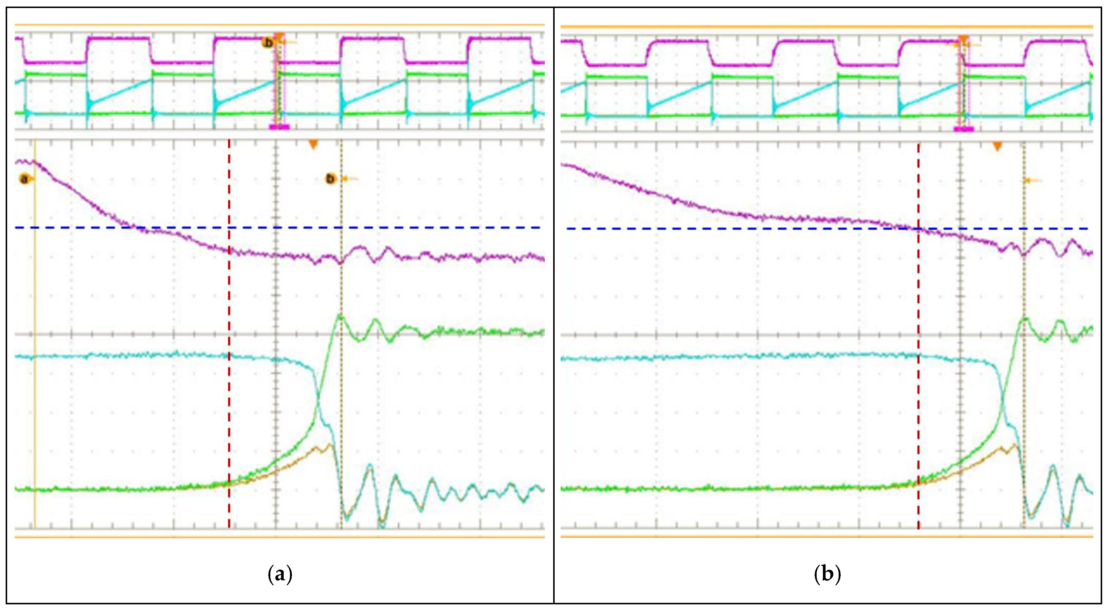
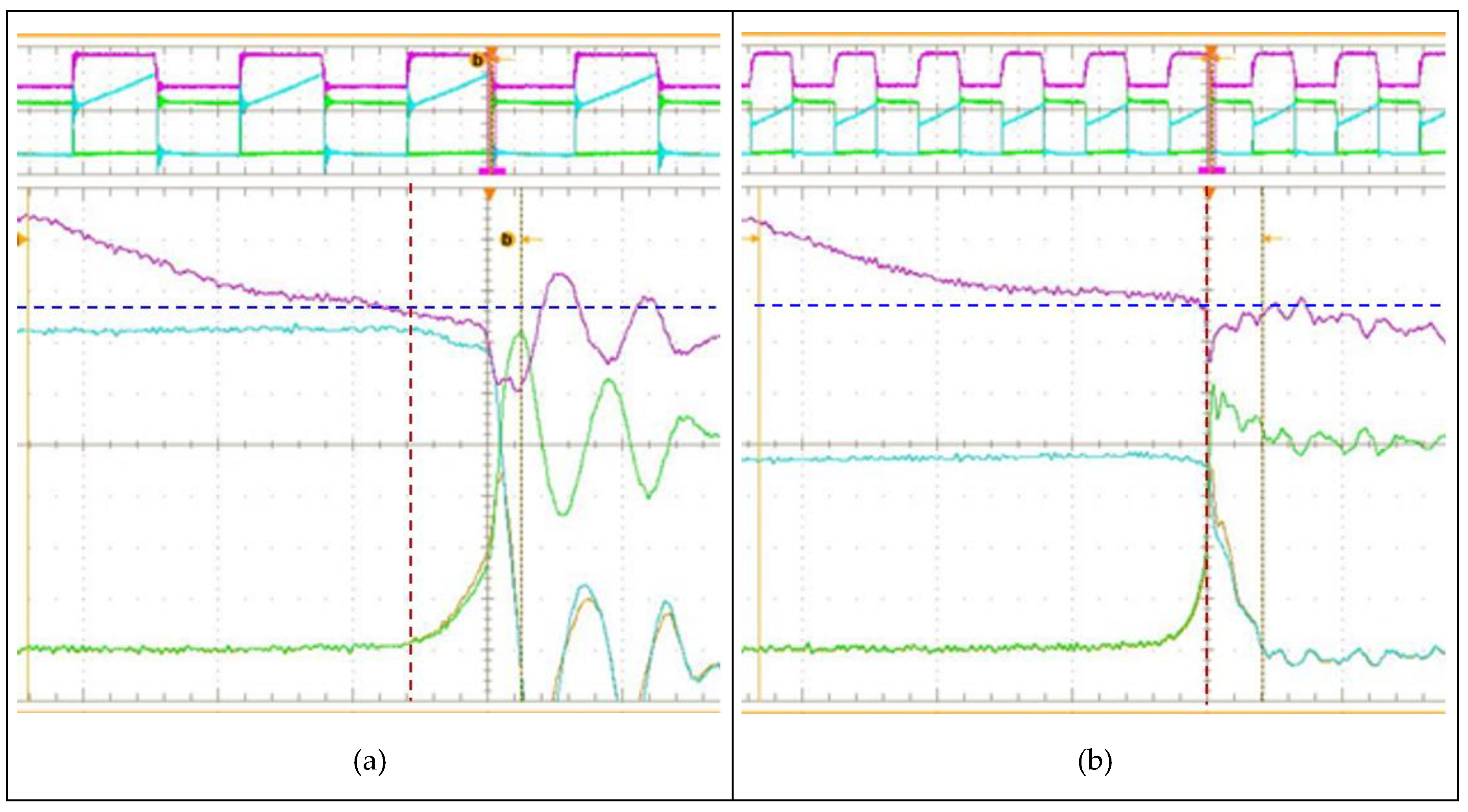
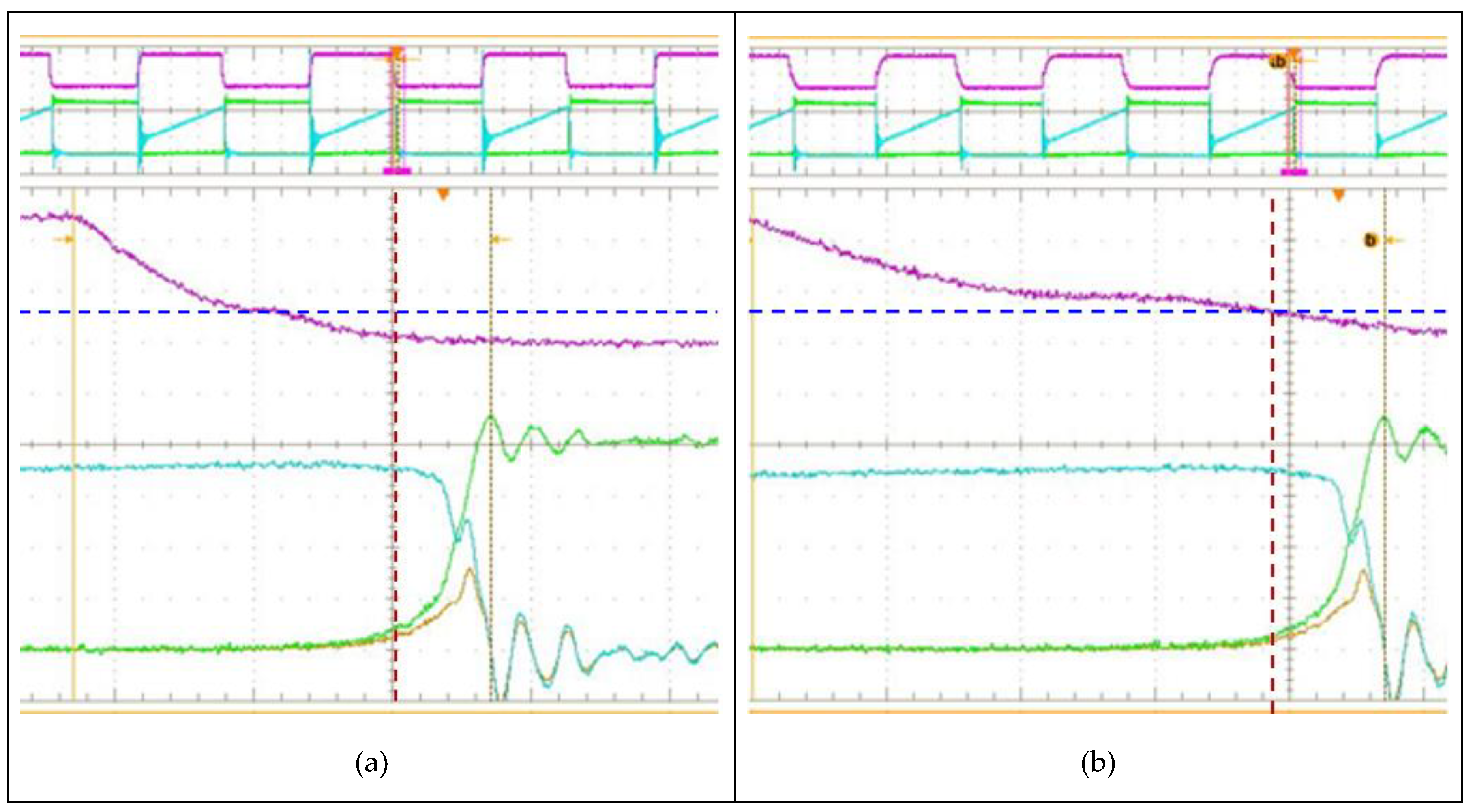
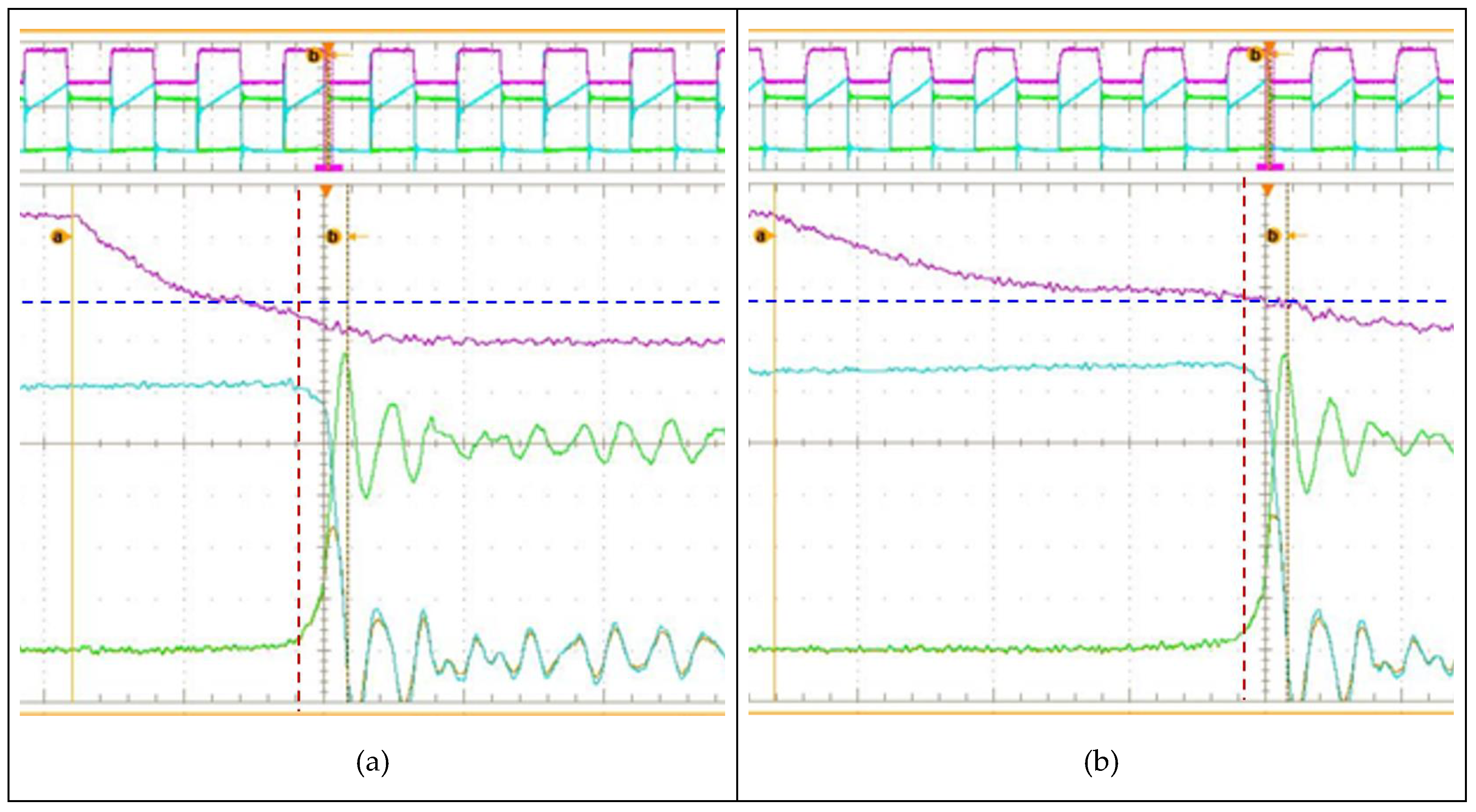
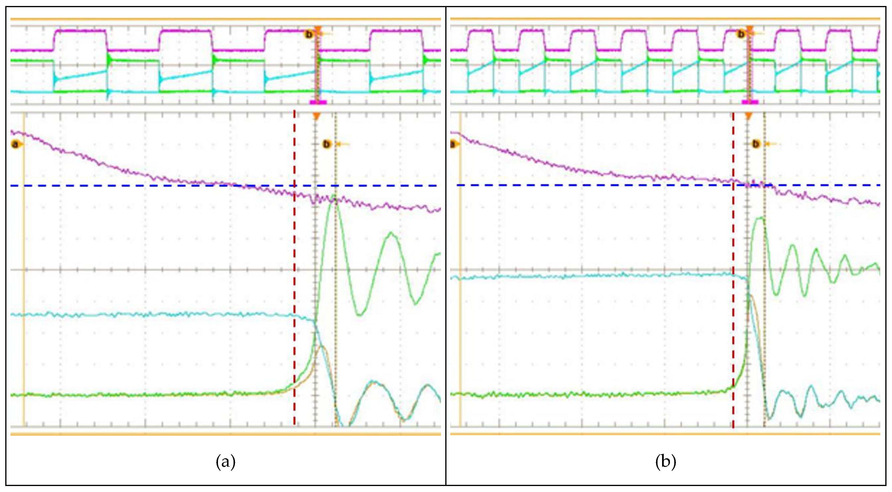
In each figure, a dashed blue line representing the voltage threshold has been added. The value of the voltage threshold accounts for its reduction with increasing MOSFET temperature, being the temperature measured in each specific operating condition reported in the figures. The dashed red line indicates where the switching losses start. Looking at the intersection between the two dashed lines, it arises that the device’s gate-source voltage (violet waveform) is below or just above the threshold voltage at the beginning (red dashed line) of the interval where the switching losses are greater than zero. Moreover, when the gate-source voltage is greater than the threshold voltage at the beginning (red dashed line), for a large part of the interval where the power losses are greater than zero the gate-source voltage is lower than the threshold one.
Therefore, the device can be modelled considering only its parasitic capacitance for the circuit analysis.
3. Turn-off circuit analysis
As reported in the literature and shown in
Figure 2, the additional turn-off switching losses in 3L MOSFET in comparison to the 4L MOSFET increase with increasing gate resistance and load. Such greater switching losses are commonly attributed to the lower switching speed of 3L MOSFET. Therefore, circuit analysis is performed in this section to obtain an analytical formulation of the current slew rate during the turn-off of 3L and 4L MOSFETs. The goal is the identification of an equation representing the effect of the gate resistance and load condition on the current slew rate for comparison purposes.
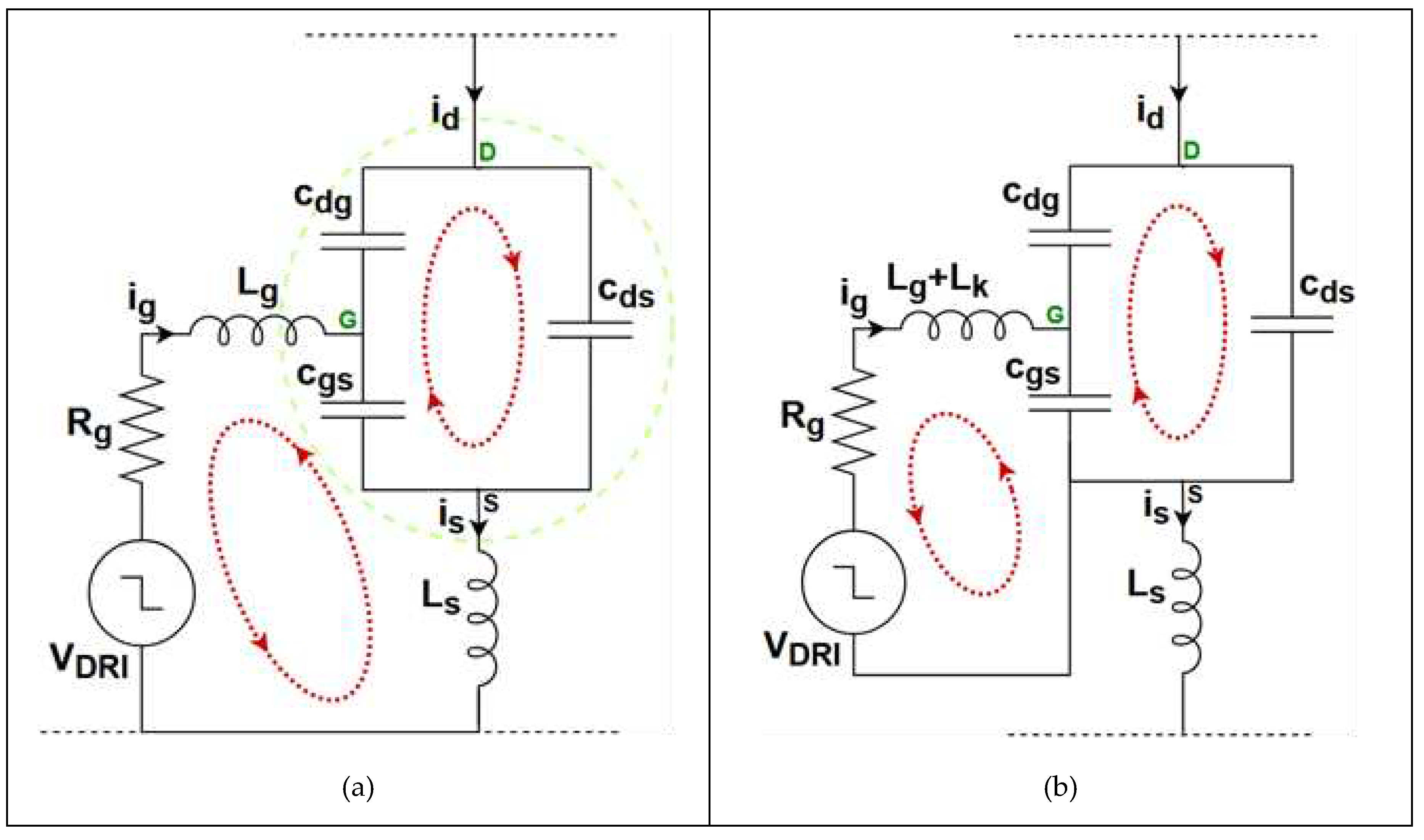
Figure 9 reports a circuit model of a 3L and 4L MOSFET embedded in the converter. According to the previous considerations based on the analysis of the waveforms, the gate-source voltage has been considered equal or below the threshold and, consequently, the voltage-controlled current generator between the drain and source is absent.
From the inspection of
Figure 9, it is apparent that the following Kirchhoff current laws (KCL) are valid for both MOSFETs.
Moreover, looking at the device parasitic capacitances loop, also the following Kirchhoff voltage law (KVL) can be considered for both MOSFETs.
By substituting this KVL in equation (1) and rearranging it, the following expression is obtained for both devices:
Similarly, by substituting the KVL in equation (2) and considering equation (4), the following expression is obtained for the gate current of both MOSFETs:
There is a key difference when the KVL related to the driving loop is considered:
Equations (6) and (7) can be, respectively, combined with the previous one to obtain the analytical expression of the current slew rate. Indeed, in the case of a 3L MOSFET, an additional equation is necessary because the source current is present in equation (6). The necessary additional equation is obtained considering the KCL related to the Gaussian surface represented by the dashed green line in
Figure 9a:
By substituting equations (5) and (8) in equation (6) and rearranging the results, the following expression is obtained for the current slew rate of a 3L MOSFET during the turn-off.
A similar equation can be obtained for the current slew rate of a 4L MOSFET by substituting equation (5) in equation (7) and rearranging the results as reported in equation (10).
In both cases, some considerations enable simplified, although less accurate, equations. In particular:
By applying these relations, equations (9) and (10) can be approximated, respectively, as follows:
These simplified equations present the same numerator while the denominator is different. The denominators in (11) and (12) represent the total inductance of the driver loop when, respectively, a 3L and a 4L MOSFET are considered. The greatest inductance in the first cases is due to the longer path, then:
Considering equation 14, and considering that the current slew rate is negative during the turn-off, then the term
in equations (11) and (12) highlights that the current slew rate increases as the gate resistance and current increase. More specifically, the improvement achieved by 4L as the
and
increase can be expressed using the following function:
which is concordant with the experimental analysis reported in
Figure 2. The increment is not linear, and it is negligible at low load due to the term
, in equations (11) and (12), which is opposite to the current reduction, and it depends on the gate resistance too.
To verify experimentally the results obtained in equations (11) and (12), an inductor,
LA, has been added to the gate path of the 4L MOSFET in
Figure 9b, so that:
The value of
LA has been properly chosen to obtain the same driving loop inductance
Under this condition, the current slew rate of the 3L and 4L MOSFETs should be similar if the theoretical aspects obtained in equations (11) and (12) are true:
In other terms, proving equation 18 is sufficient to prove equations (11) and (12).
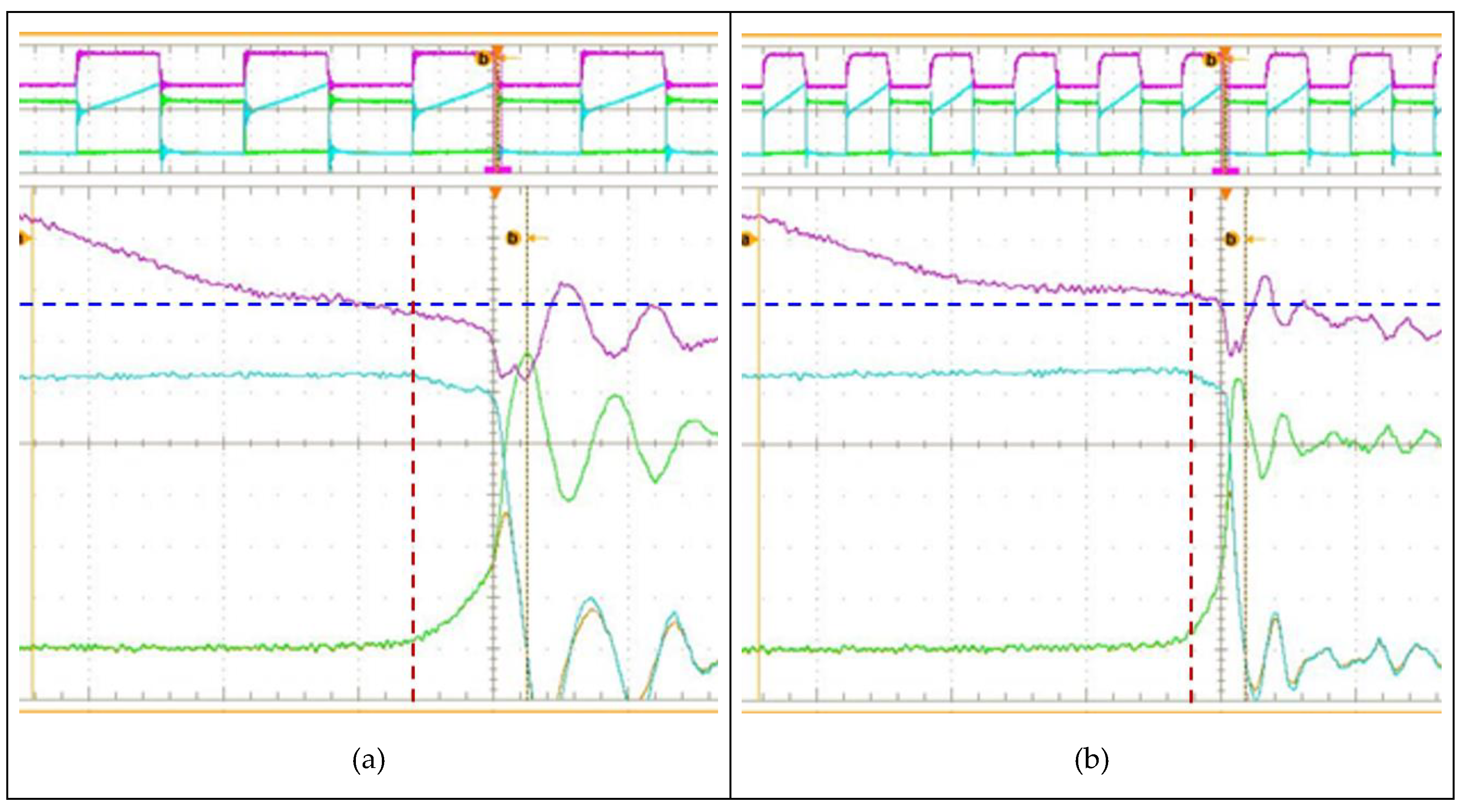
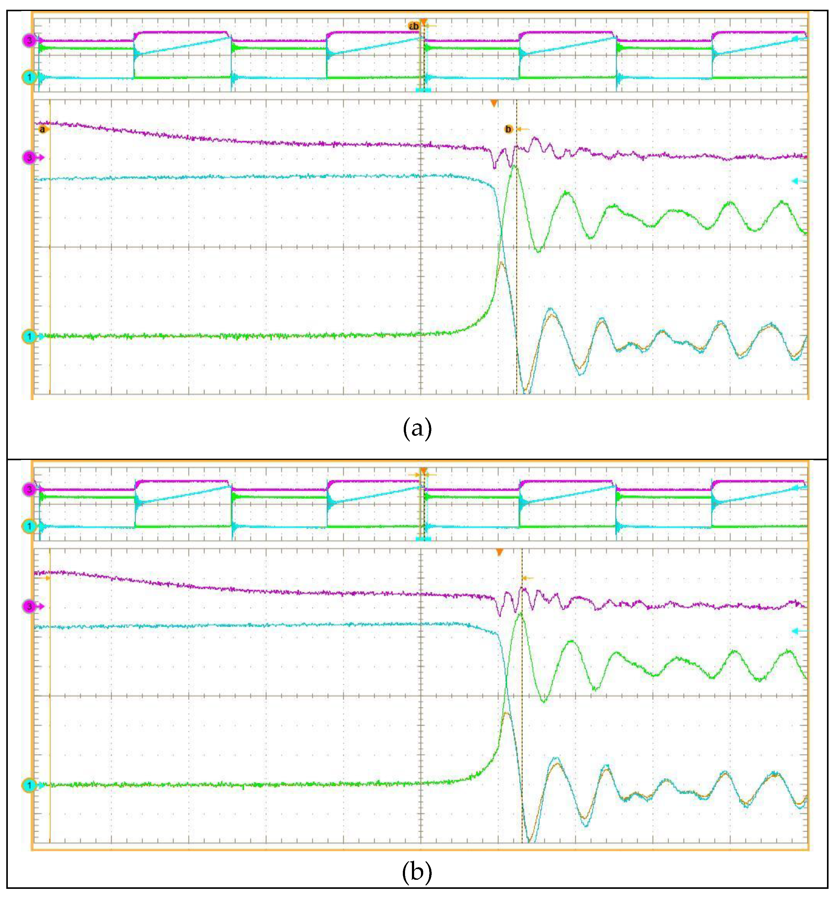
Figure 10 show the waveforms obtained for 3L (a) and 4L (b) when
LA is added to the gate path of the 4L MOSFET in
Figure 9b, and its inductance has been chosen according to equation 17. The figures confirm that, under this condition the current slew rate is similar, thus proving the theoretical results.
5. Conclusions
The SuperJunction MOSFETs empowered by the addition of the Kelvin pin - 4L MOSFETs - present lower switching losses than the 3L counterpart. The maximum difference between the switching losses of the two MOSFETs is obtained at a high load. This makes the 4L MOSFETs the best choice in high-power density applications when substantial load currents have to be considered.
In this work, the turn-off switching losses of 3L and 4L MOSFETs have been first experimentally compared. Then, circuit models and Kirchhoff laws have been adopted to obtain simplified analytical expressions of the MOSFETs’ current slew rate.
These expressions have highlighted the reasons behind the improvements obtained by adopting 4L MOSFET during the turn-off. The key information that emerged is that the turn-off improvement obtained by adopting the Kelvin source is due to the lower inductance of the driver loop in comparison with the power loop inductance instead of the decoupling between these loops. This result has also been experimentally confirmed by adding an inductor to the gate loop of the 4L to achieve a similar total inductance drive loop for 3L e 4L. Under this condition, the same current slew rate has been found, thus confirming the theoretical expressions.
Finally, the circuit analysis and the aforementioned expressions have explained the reasons behind the increment of the difference of the turn-off losses between 3L and 4L with increasing the gate resistance and load current.
Acknowledgments
This research was partially funded by Ministry of Education, Universities and Research (Italy) under the call PRIN 2017 grant number 2017MS9F49.
Conflicts of Interest
The authors declare no conflict of interest.
References
- M. Gepp, R. Filimon, S. Koffel, V. R. H. Lorentz and M. März, "Advanced thermal management for temperature homogenization in high-power lithium-ion battery systems based on prismatic cells," 2015 IEEE 24th International Symposium on Industrial Electronics (ISIE), 2015, pp. 1230-1235. [CrossRef]
- M. Noah et al., "A novel three-phase LLC resonant converter with integrated magnetics for lower turn-off losses and higher power density," 2017 IEEE Applied Power Electronics Conference and Exposition (APEC), 2017, pp. 322-329. [CrossRef]
- Disney, D.; Shen, Z.J. Review of Silicon Power Semiconductor Technologies for Power Supply on Chip and Power Supply in Package Applications. IEEE Trans. Power Electron. 2013, 28, 4168–4181. [Google Scholar] [CrossRef]
- Beres, R.N.; Wang, X.; Liserre, M.; Blaabjerg, F.; Bak, C.L. A Review of Passive Power Filters for Three-Phase Grid-Connected Voltage-Source Converters. IEEE J. Emerg. Sel. Top. Power Electron. 2015, 4, 54–69. [Google Scholar] [CrossRef]
- Yeh, C. -S.; Chen, C. -W.; Lee, M.; Lai, J. -S. A Hybrid Modulation Method for Single-Stage Soft-Switching Inverter Based on Series Resonant Converter. IEEE Transactions on Power Electronics 2020, 35, 5785–5796. [Google Scholar] [CrossRef]
- K. Gupta et al., "Thermal Management Strategies for a High-Frequency, Bi-Directional, On-Board Electric Vehicle Charger," 2018 17th IEEE Intersociety Conference on Thermal and Thermomechanical Phenomena in Electronic Systems (ITherm), 2018, pp. 935-943.
- S. Anwar, W. Zhang, F. Wang and D. J. Costinett, "Integrated DC-DC converter design for Electric Vehicle powertrains," 2016 IEEE Applied Power Electronics Conference and Exposition (APEC), 2016, pp. 424-431.
- Yang, S.; Xiang, D.; Bryant, A.; Mawby, P.; Ran, L.; Tavner, P. Condition Monitoring for Device Reliability in Power Electronic Converters: A Review. IEEE Trans. Power Electron. 2010, 25, 2734–2752. [Google Scholar] [CrossRef]
- R. Jagannathan, H. -P. Hoenes and T. Duggal, "Impacts of package, layout and freewheeling diode on switching characteristics of Super Junction MOSFET in automotive DC-DC applications," 2016 IEEE International Conference on Power Electronics, Drives and Energy Systems (PEDES), 2016, pp. 1-6.
- M. Cacciato et al., "Analysis of the different impact of the external Gate Resistance in 3-lead and 4-lead SuperJunction MOSFETs," 2021 AEIT International Annual Conference (AEIT), 2021, pp. 1-6. [CrossRef]
- F. Giorgio, S. A. Rizzo, N. Salerno, G. Scarcella, A. Scuto and G. Sorrentino, "Understanding the Kelvin pin mitigation of the MOSFET turn-on losses by fast-switching and neutralization of the clamp diode," IECON 2021 – 47th Annual Conference of the IEEE Industrial Electronics Society, 2021, pp. 1-6. [CrossRef]
|
Disclaimer/Publisher’s Note: The statements, opinions and data contained in all publications are solely those of the individual author(s) and contributor(s) and not of MDPI and/or the editor(s). MDPI and/or the editor(s) disclaim responsibility for any injury to people or property resulting from any ideas, methods, instructions or products referred to in the content. |
© 2023 by the authors. Licensee MDPI, Basel, Switzerland. This article is an open access article distributed under the terms and conditions of the Creative Commons Attribution (CC BY) license (http://creativecommons.org/licenses/by/4.0/).
