1. Introduction
High-speed electric motor drive systems have gained significant popularity in various industries due to their compact size, lightweight design, and impressive power density. These systems operate at exceptionally high fundamental frequencies (), typically in the kilohertz range, necessitating inverters capable of handling such demanding switching frequencies.
However, traditional silicon (Si) IGBT technology has limitations in achieving high switching frequencies, resulting in compromised current quality at higher fundamental frequencies. The decrease in the frequency modulation index (
) with increasing fundamental frequency leads to higher total current harmonic distortion (THD) [
1]. Additionally, Si-IGBT technology exhibits drawbacks in terms of efficiency, operating temperature, and power density.
To overcome these limitations, SiC MOSFET technology has emerged as a superior alternative to Si-IGBT technology. SiC MOSFETs offer advantages such as higher efficiency [
2,
3,
4], increased switching frequency, extended operating temperature capabilities [
5,
6], and improved power density [
7]. These properties make SiC MOSFETs a preferred choice for high-speed electric motor drive systems, surpassing the limitations of Si-IGBT technology.
In this context, SiC-based inverters have been identified as suitable for high-speed machines requiring high fundamental and switching frequencies to minimize total harmonic distortion of the current [
8]. The voltage deviation and current distortion in the inverter are directly proportional to the increasing
.
This research aims to model, study, and compare the influence of various parameters, including dead-time, switching delay time, voltage drop, and parasitic capacitor output, on voltage and current distortion in SiC-based and IGBT-based inverters for high-speed machines. The fundamental frequencies tested range up to 3400 Hz, while the switching frequencies vary from 10 kHz to 100 kHz.
The remainder of this paper is organized as follows.
Section 2 presents the proposed analytical model.
Section 3 explores the influence of imperfections in the considered components in detail.
Section 4 presents the experimental results. Finally, the conclusion is provided in the last section.
2. Analytical Modeling of a three-phase voltage source inverter and Imperfections
2.1. Three-phase voltage source inverter modeling
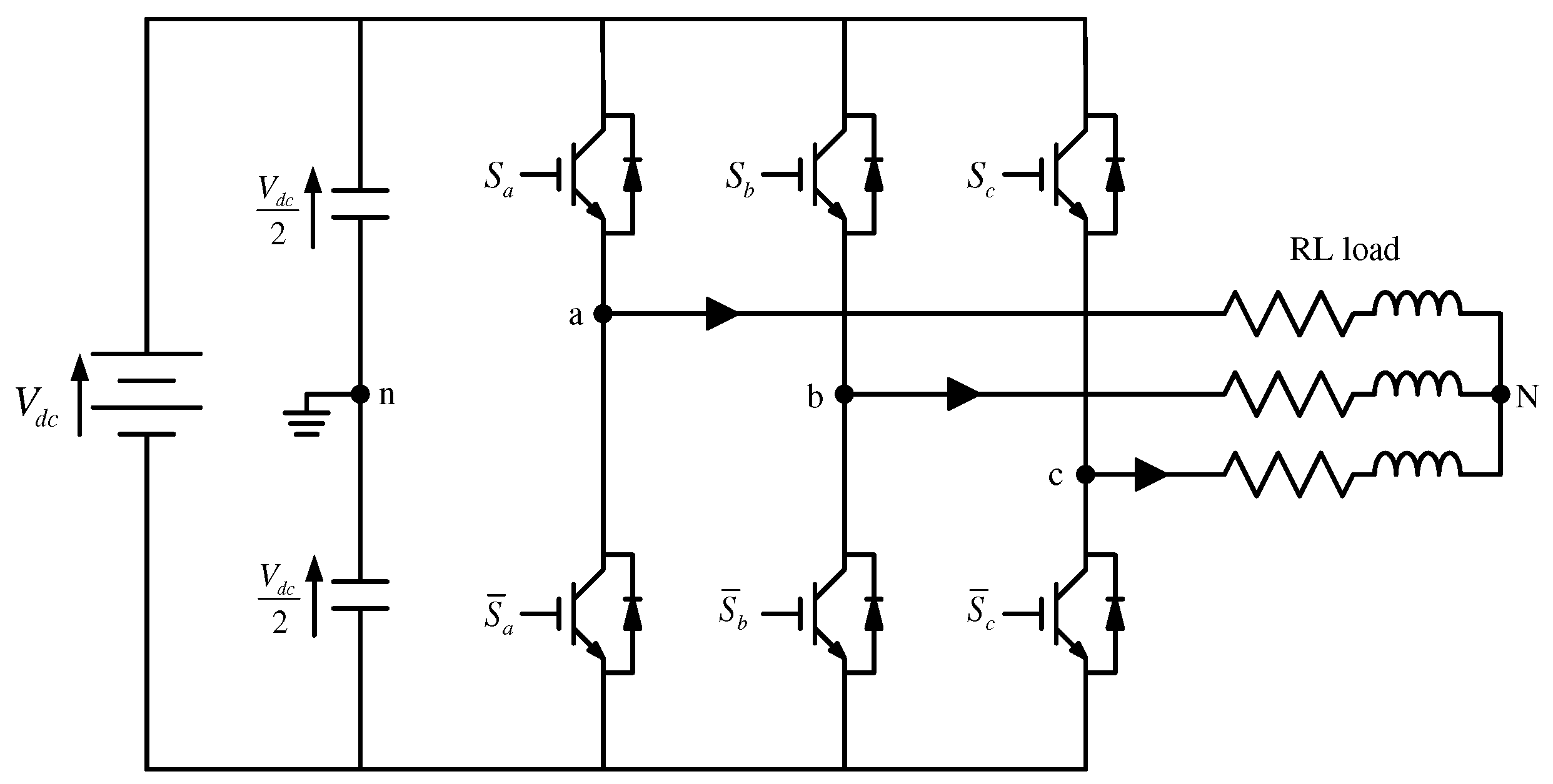
Figure 1 illustrates a three-phase voltage source inverter (3Ph-VSI) used for general applications. In this figure, the load current is positive when it flows from the source to the load, and negative when it reverses its direction.
The modeling of the 3Ph-VSI is initially developed without considering imperfections such as dead times, delays in component startup and shutdown, voltage drops, and parasitic capacitances. Therefore, the ideal switching function can be written as a simple arithmetic relationship between the control signals of the switches defined in
Figure 1, such that
(where
). Consequently, the voltages
can be expressed as follows:
2.2. Analytical Modeling of Imperfections
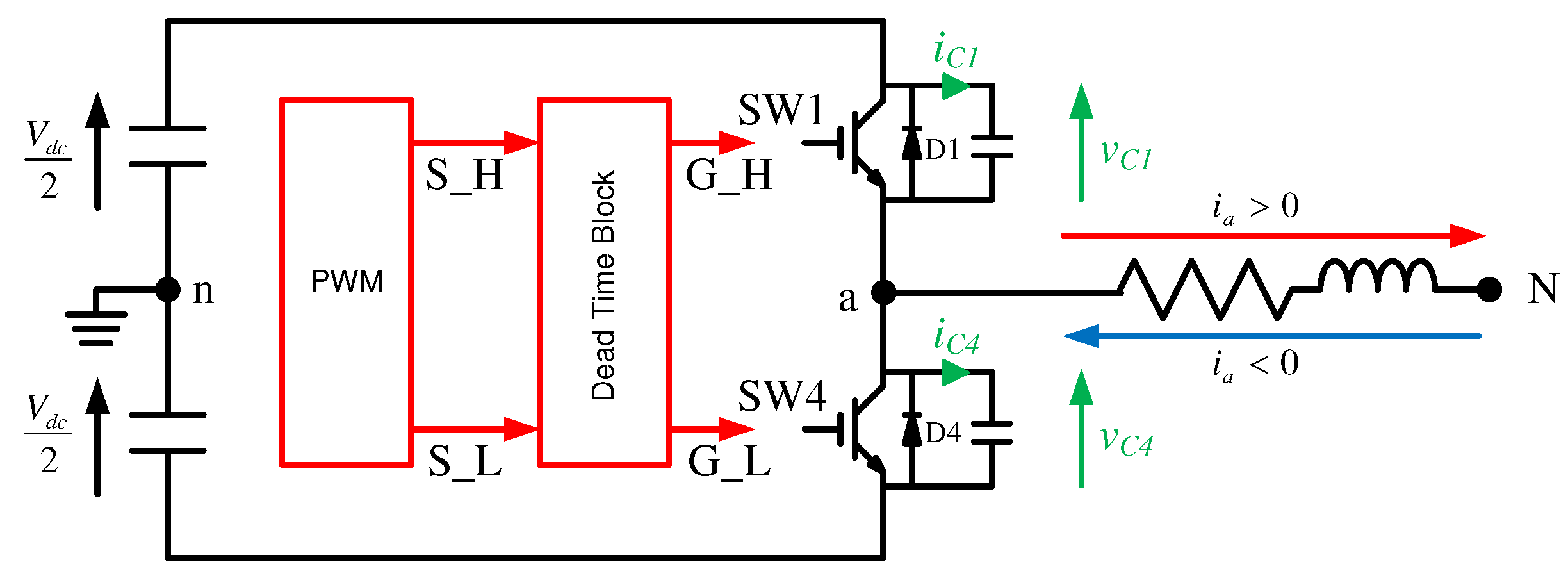
In this section, an analytical model will be developed to consider various imperfections in a 3Ph_VSI. Factors such as dead times between switching signals, switching times, voltage drops caused by power switches (IGBT, SiC, diode), and the effects of parasitic capacitances will be taken into account. The focus of the study is on analyzing one leg of the VSI, as illustrated in
Figure 2.
In the following, the distortion voltage due to imperfections is defined as
, which is the difference between the actual output voltage (
) and the ideal output voltage (
), corresponding to a perfect inverter:
where
is the average voltage drop over one modulation period (PWM) due to dead times,
is the average voltage drop due to component switching times,
is the average voltage drop due to voltage drops across power switches,
is the average voltage drop caused by the effects of parasitic capacitances.
2.2.1. Dead time effect
Ideally, based on
Figure 2, the power switches S1 and S4 are controlled by PWM signals (
,
). In reality, a dead time (
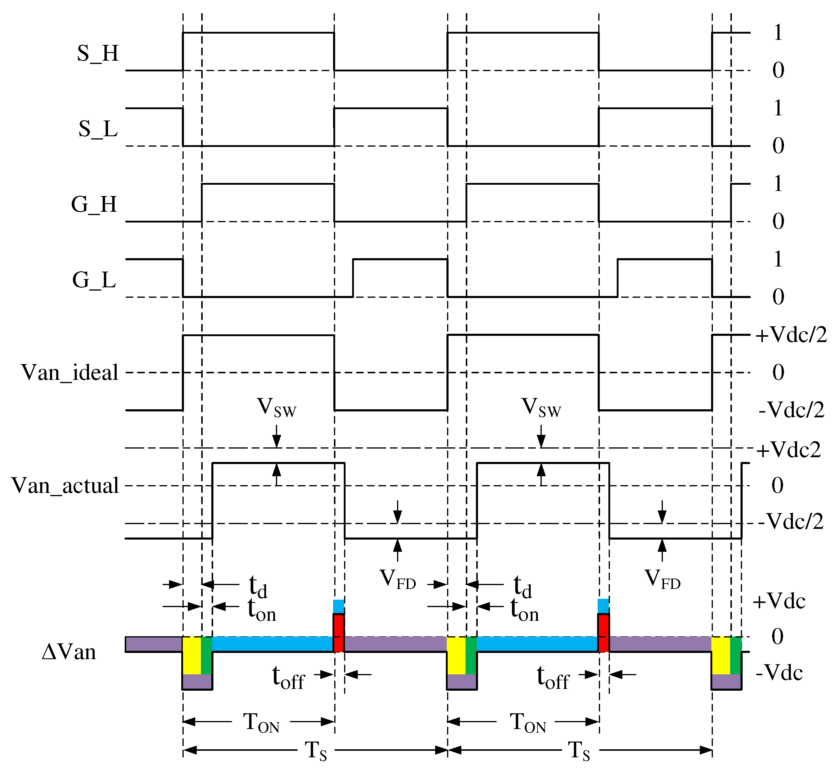
) needs to be introduced where both S1 and S4 turn off at the same time to prevent a short circuit from occurring through S1 and S4. During the dead time interval, the phase current flows through diode D4, resulting in an output voltage equal to
when the current is positive (
). When the current is negative (
), the phase current flows through diode D1, causing the output voltage to become positive
. The average voltage drop caused by the dead time (the yellow area in
Figure 3) can be expressed as follows:
The relation (
3) demonstrates that the average voltage drop induced by the dead time is proportional to the ratio
. When the PWM frequency is increased (
is decreased), the voltage drop becomes more significant if the dead time cannot be reduced in the same proportion due to limitations imposed by the drivers or the power switches (IGBT or SiC). The average distortion voltage at the terminals of phase "a" induced by the dead time can be expressed, based on equation (
3), according to the directions of the three phase currents, as follows:
2.2.2. Rise time and down time effect
The switching of power electronic components is not instantaneous. In practice, it takes a certain amount of time for a switch to turn on and a certain amount of time to ensure its blocking. These switching times accumulate with the dead time defined in the previous section and must be considered to accurately determine the waveform of the voltage
. Therefore, when
, the average voltage drop induced by the switching times
(green area in
Figure 3) and
(red area in
Figure 3) can be expressed as follows:
Where:
is the turn-on time (), with being the propagation time at turn-on, and being the rise time (from to ).
is the turn-off time (), with being the propagation time at turn-off, and being the fall time (from to ).
From equation (
5), the voltage drop across phase "a" induced by the switching times can be expressed based on the directions of the three phase currents as follows:
2.2.3. Consideration of voltage drops in components
In power electronic systems, voltage drops across components like power switches (IGBT, SiC) and diodes should be taken into account. These voltage drops depend on the direction of the phase current. Let
represent the voltage drop across a conducting switch, identified by the blue area in
Figure 3. With this in mind, the following relationship can be formulated:
With
, which represents the voltage drop across the conducting switch, where
is the forward voltage drop of the switch and
is the on-state resistance of the switch. When calculating the voltage drop, the current
is assumed to remain constant over a PWM period. As illustrated in
Figure 3 when
and
is in a low state while
is in a conducting state, the current then flows through diode D4. During this conduction phase, the output voltage
takes the following value:
With
, which represents the voltage drop across the conducting diode, where
is the forward voltage drop of the diode and
is the on-state resistance of the diode. When calculating the voltage drop, the current
is assumed to remain constant over a PWM period. By combining the both terms, the average output voltage drop resulting from the voltage drops in the components can be rewritten as a function of the sign of the current in the corresponding phase (in this case, phase a).
The average voltage drop across phase "a" induced by the voltage drops in the components can be expressed in terms of the directions of the three-phase currents as follows:
2.3. Effects of Parasitic Capacitance
Power semiconductor models (IGBT, SiC) exhibit parasitic capacitances, particularly the output capacitance between the emitter and collector for IGBTs, and between the drain and source for SiC, as shown in
Figure 2. These capacitances, with values around a few nF, influence switching and affect output voltage distortion during dead times, depending on the switch type (IGBT or SiC), and also include wiring parasitic capacitances.
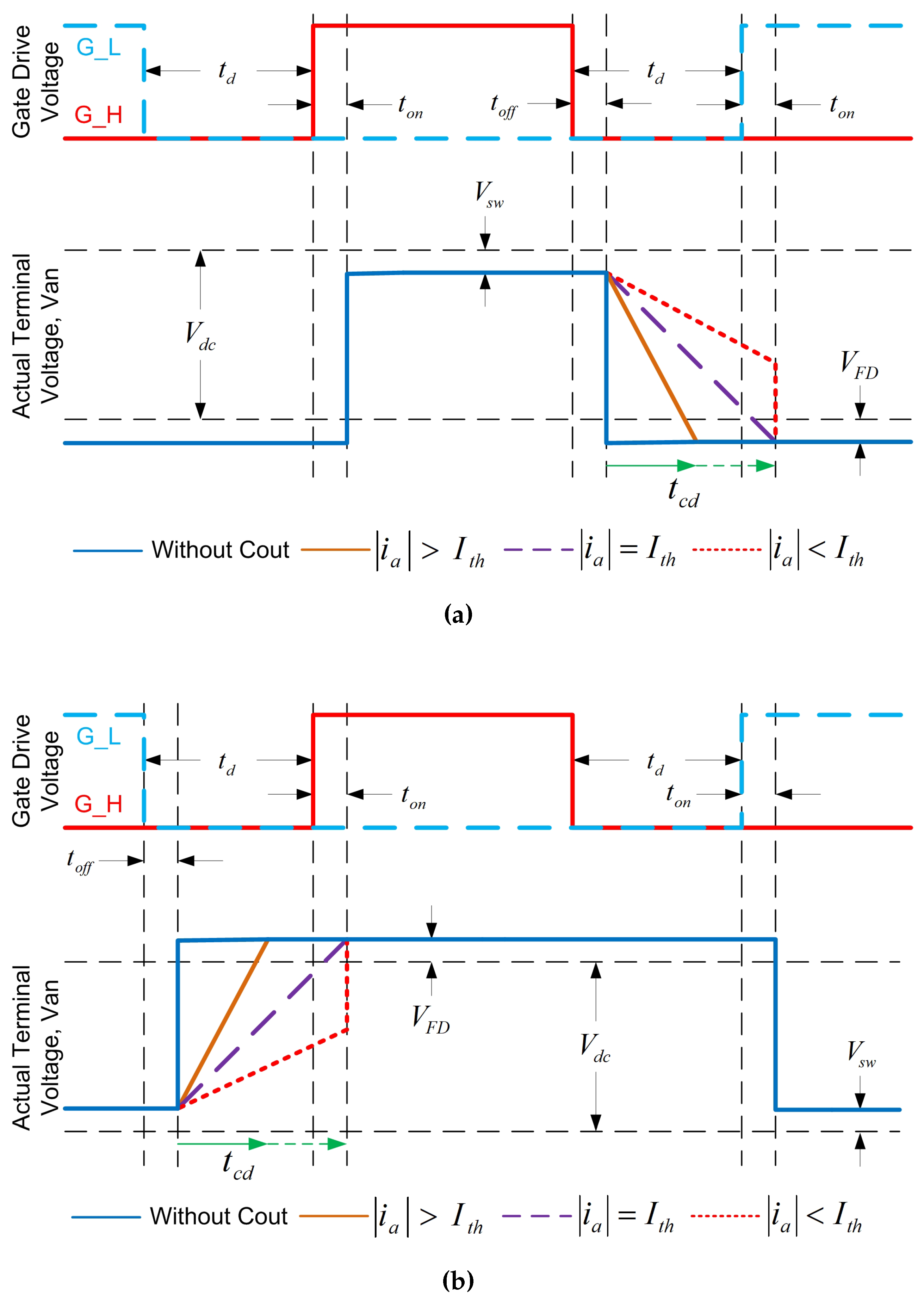
In
Figure 4, when the phase current flows in the positive direction, during the on period (S1 is ON), the phase current flows through S1. Then the voltage across the inverter becomes
and the bottom parasitic capacitance (
) is charged. During the dead time interval, the top parasitic capacitance (
) starts charging and
discharges to let the phase current flow. Thus, the voltage across the inverter becomes
. Then,
discharges and the voltage of
(
) reaches zero (
). At this point, the phase current (
) can be expressed as the sum of the charge current (
) and the discharge current (
). Assuming that
,
are equal (
), where
is the total parasitic capacitance, which depends on both the transistor parasitic capacitance and the external capacitance due to the cable’s connection. The charge or discharge time (
) of the parasitic capacitor is represented by:
The current for charging (or discharging) the capacitance in the actual dead time interval (
) of
Figure 4 is called the threshold current (
) and is given by:
Three situations where the absolute value of the phase current (
) is more than
(
, brown line), equal to
(
, purple line) and less than
(
, red line), are illustrated by
Figure 4.
The orange areas of
Figure 3 shows the voltage drop caused by the parasitic capacitors, then considered as expressions obtained as a function of the phase current [
9,
10,
11,
12].
When :
The average voltage drop due to parasitic capacitances,
, can be rewritten as a function of the sign of the current in the corresponding phase (in this case, phase a).
with
In a general sense, the amplitude of the threshold current (
) is much lower than the phase current magnitude
. As a result, the relationship (
17) can be simplified as follows:
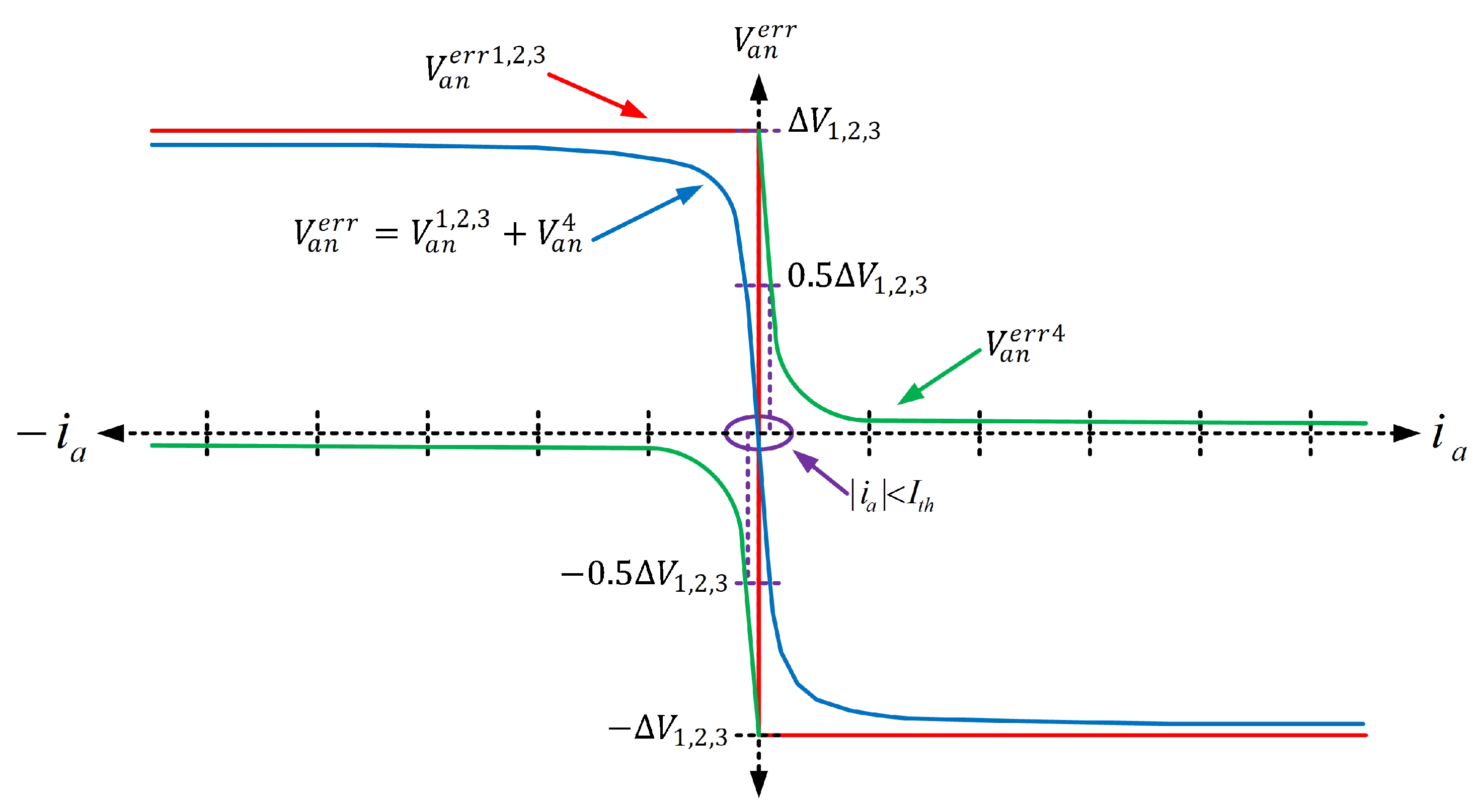
The variations of
with respect to the values taken by the phase current
are then represented in green in
Figure 5 (curve in
for
). The voltage drop caused by other imperfections,
(dead times, switching times, and voltage drop in components), is also depicted in red on this figure, along with the resulting voltage drop shown in blue. It can be observed that the parasitic capacitances have a beneficial effect on the voltage drop, leading to lower values, but this depends on the magnitude of the load current.
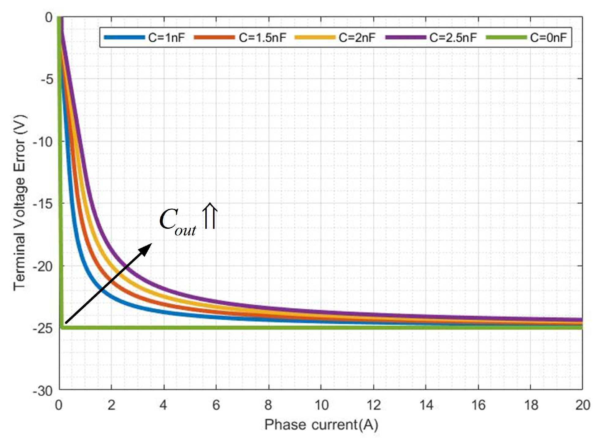
Figure 6 shows the impact of the parasitic capacitance value on the overall voltage drop (limited to
). A larger parasitic capacitance limits the voltage drop for low currents, but it has little effect on the average global voltage drop at the inverter output for higher currents.
The average voltage drops resulting from different imperfections of the inverter have been derived in this section. Consequently, the total voltage drop across phase "a" can be expressed as follows:
where
Finally, based on equation (
1), this voltage drop can be expressed for all three phases, depending on the signs of the respective currents.
3. The influence of imperfections on the output voltage of the inverter
The previous section discussed the average voltage drops resulting from imperfections in the inverter. These imperfections will have two key effects. Firstly, there will be a voltage drop in the RMS value of the fundamental component of the inverter’s output voltage. Secondly, the imperfections will generate additional voltage harmonics that will affect the load current, especially the low-frequency harmonics. These effects will be further examined in the following section.
3.1. RMS value of the fundamental component of the output voltage
The RMS value of the fundamental component at the terminals of a phase (
) can be derived by considering the modulation index (
) and the DC bus voltage (
):
In the case of an inductive load with a phase lag of
, the RMS value of the distortion in the phase voltage
can be expressed as follows:
Where the term
has been defined in equation (
20) and encompasses all the voltage drops resulting from the imperfections of the inverter. The value of the voltage drop
can be evaluated based on the measurement of
.
The voltage represents the fundamental component of the voltage across phase "a" that would occur in the absence of any imperfections.
3.2. Harmonics generated by the inverter’s imperfections
The literature focuses on the impact of dead times on harmonic amplitudes, leading to complex formulas [
13,
14,
15]. Dead times increase harmonics and decrease the fundamental. THD of output voltage increases linearly with dead time. Dead times also generate low-frequency harmonics, harder to filter and harmful for synchronous machines [
16]. The presence of these low-frequency harmonics is explained based on the voltage
and its spectral decomposition is given by:
where
is defined in equation (
20),
n represents the harmonic order (
), and
is the fundamental frequency. The following relationship is obtained through the development of calculations:
Low-frequency harmonics will be introduced into the voltage across the load due to inverter imperfections. In the following section, these low-frequency harmonics will be experimentally demonstrated.
4. Experimental results
To confirm the validity of our study, experimental tests were conducted on three different switches, including two IGBTs and one SiC MOSFET. The parameters of the switches are provided in
Table 1.
Table 2 presents the specification of the 3Ph-VSI.
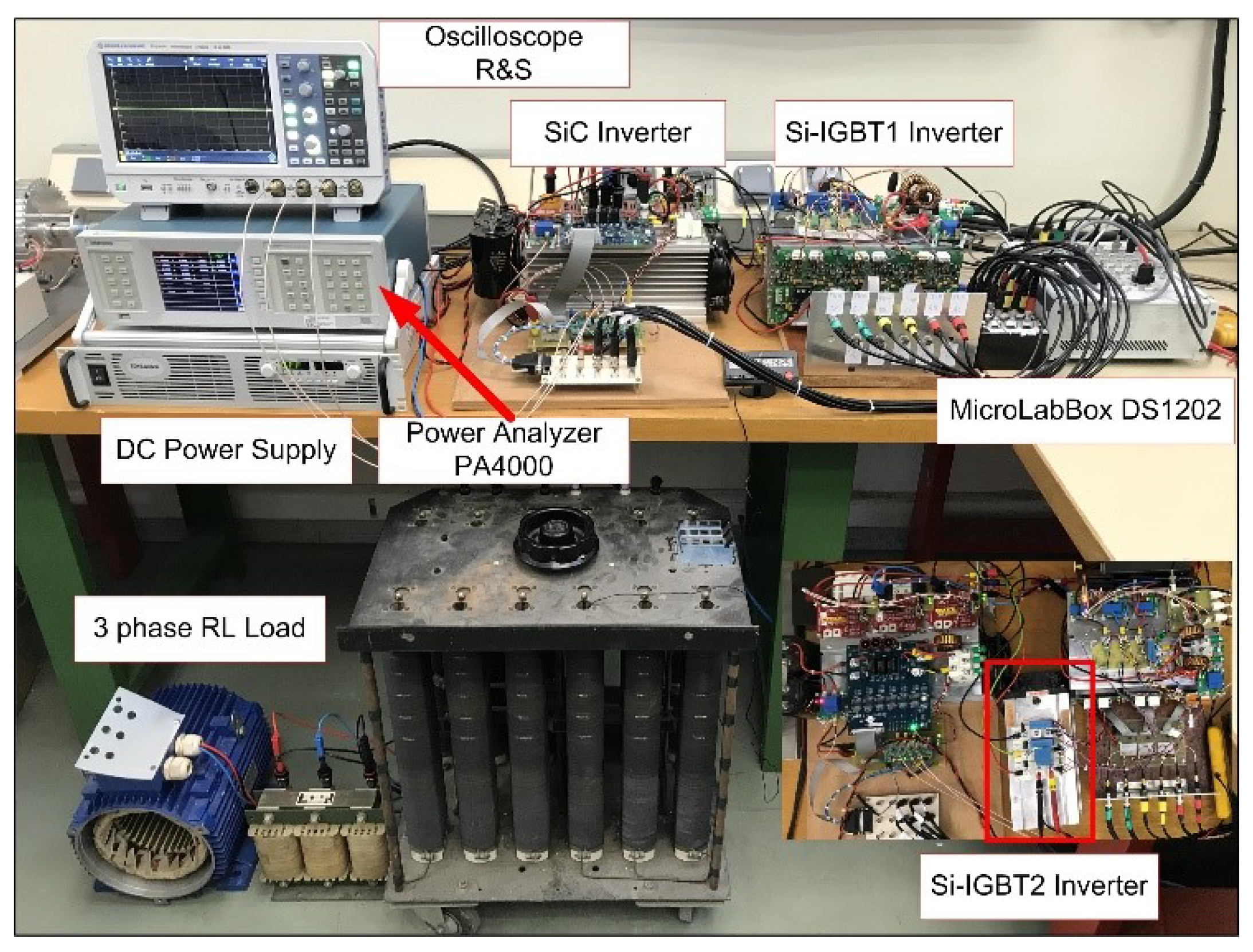
The test bench is consists of the 3Ph-VSIs, a TDK Lambda 600V, 6000W DC source, a power analyzer Tektronix
, a dSPACE MicroLabBox to control the system, a three-phase RL load (
, 3mH) and a 100 MHz Rohde & Schwarz oscilloscope. The test bench is depicted in
Figure 7.
Achieving a high switching frequency (beyond 40 kHz) utilizing the Matlab / Simulink / dSPACE RTI approach proved unattainable. Consequently, an alternative course was pursued by employing C language programming and dSPACE RTLib [
17] to program the MicroLabBox. The vector control routine finds its implementation within an Interrupt Service Routine (ISR) operating at half of the switching frequency. In order to facilitate meticulous comparisons, open loop tests were conducted, entailing the application of constant reference voltages.
4.1. Analysis of switching events for the SiC-MOSFET inverter
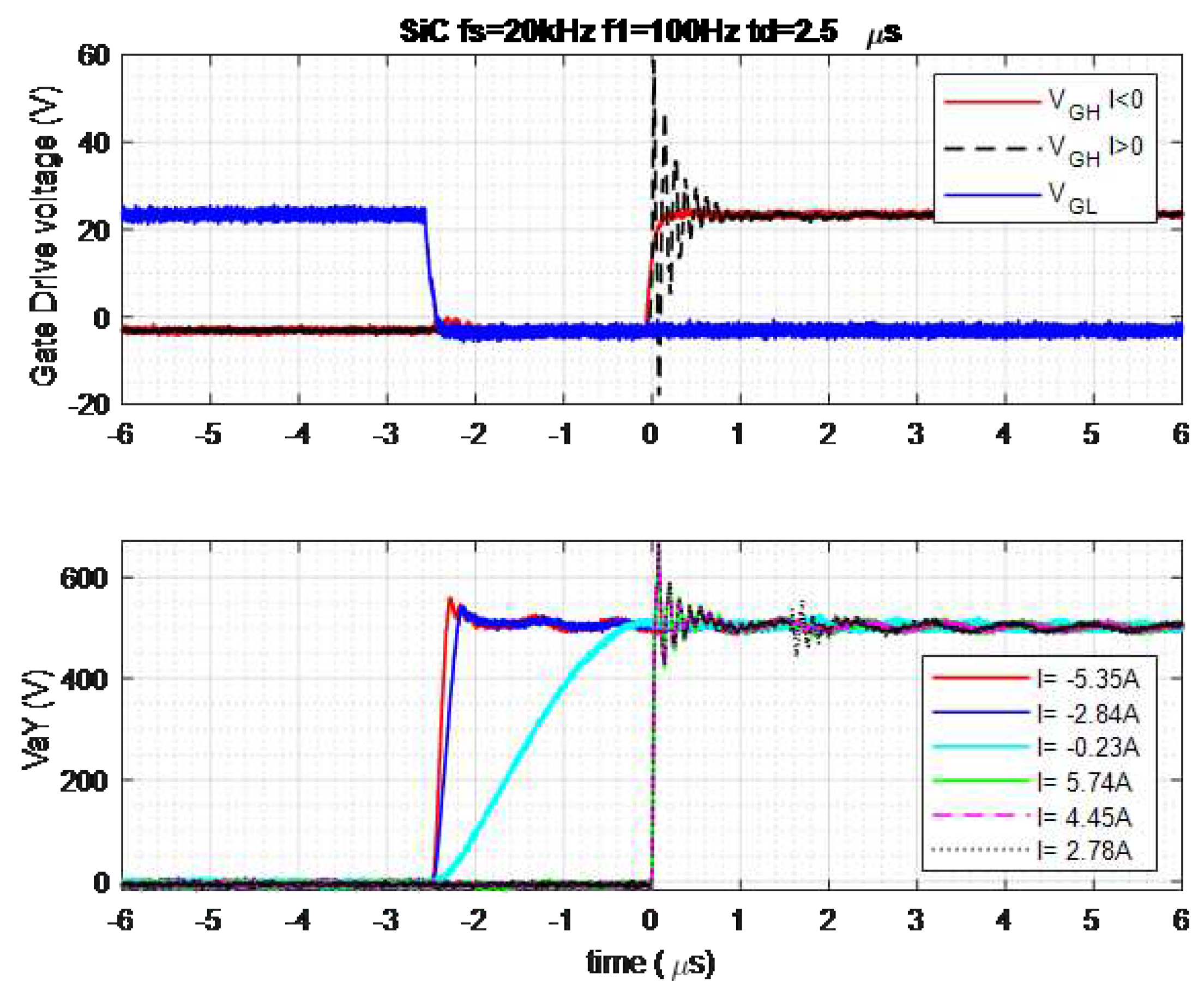
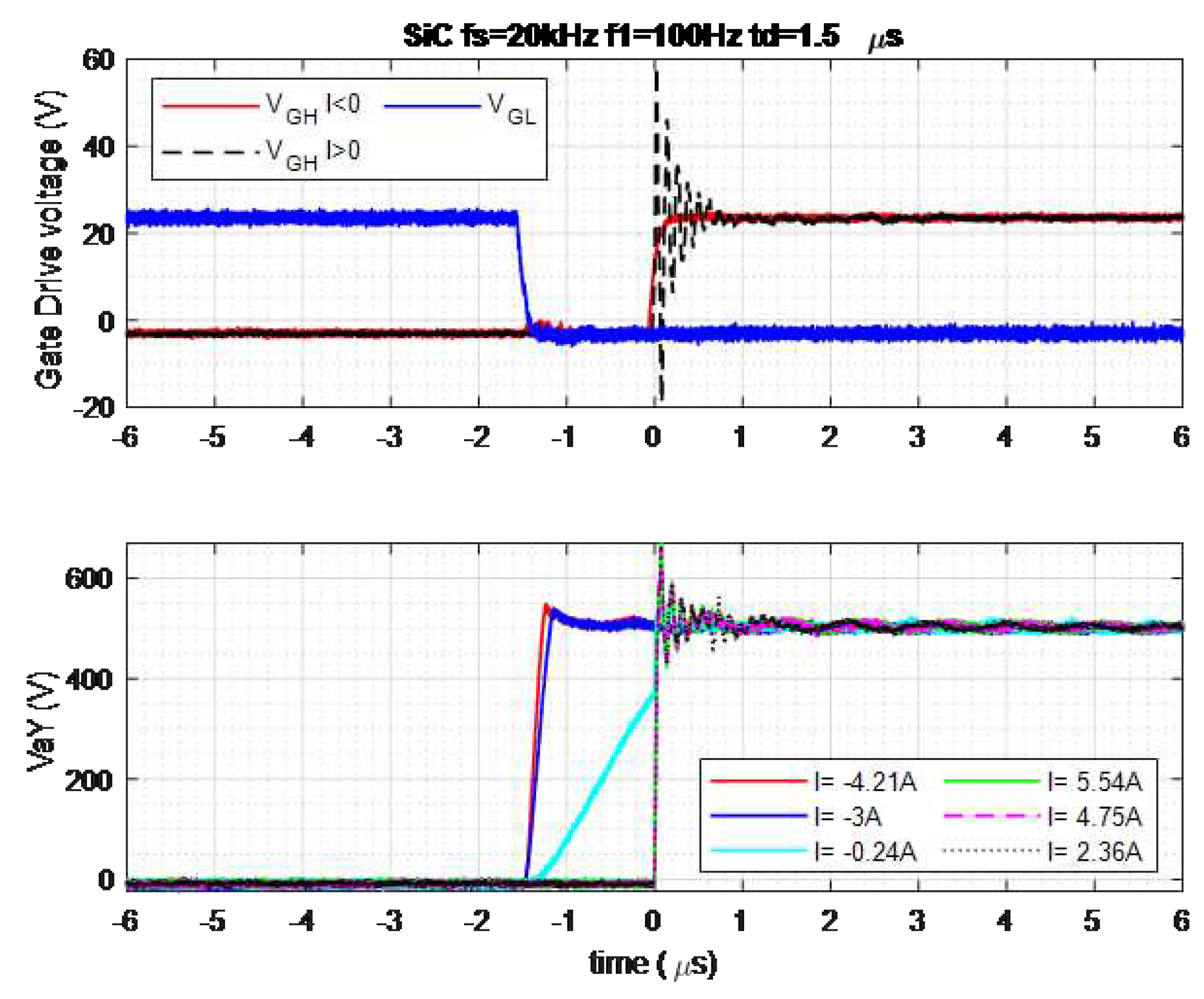
Figure 8 displays the measurements obtained for the SiC-MOSFET inverter with a dead time (
) set at
during the turn-on of switch
. The measurements were taken for various current values at the time of switching (positive or negative current).
Figure 8 shows the conduction of switch
and the blocking of switch
. The gate control signals change, affecting the voltage of the
(
see
Figure 2) depending on the current direction and magnitude during switching. High negative currents cause a rapid
rise, while lower currents slow it down. A specific case matches
rise time with the dead time. Positive currents result in a
jump after the dead time due to switch
activation. These results align with the theoretical study.
The theoretical studies were validated by reducing the dead time from
to
. The results in
Figure 9 show that, at low current values (cyan curves), the parasitic capacitance cannot be fully charged or discharged before the end of the dead time, resulting in a voltage
discontinuity during switching.
4.2. Measurement of the value of parasitic capacitances
The relationship between
(assumed
), the constant current magnitude
at switching, the discharge time (
), and the voltage variation (
) across the component can be expressed as follows:
The curves in
Figure 10 (a) for SiC-MOSFET,
Figure 10 (b) for IGBT1, and
Figure 10 (c) for IGBT2 were used to determine
for each inverter. The discharge time, voltage variation, and current magnitude at switching were recorded from the cyan-colored curves. It was observed that the voltage variation appeared to be linear for the SiC and IGBT2 inverters, consistent with model assumptions. However, for the IGBT1 inverter, the slope increased at lower voltages. Although some studies suggest an increase in parasitic capacitance with decreasing voltage, this phenomenon will be disregarded to maintain a simple model.
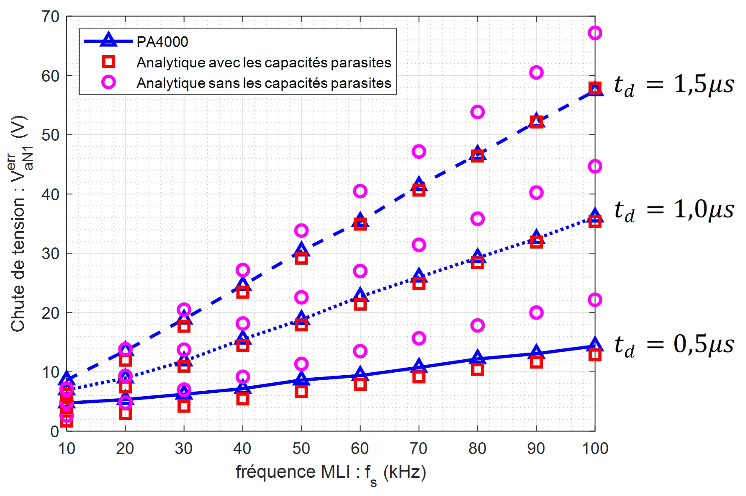
The impact of parasitic capacitances on the voltage drop and model accuracy was studied.
Figure 11 shows the voltage drop evolution with PWM frequency for three different dead time values. The theoretical curves were plotted with and without parasitic capacitance effects and compared to PA4000 measurements.
Neglecting parasitic capacitances in the modeling leads to an evident overestimation of the voltage drop, averaging around 15%. Considering these capacitances allows for highly accurate voltage drop estimation when compared to actual measurements. Thus, ignoring this phenomenon hampers correct prediction of a three-phase inverter’s output voltage value.
4.3. Comparison of the performances of the 3 inverters
The SiC-MOSFET inverter exhibits the highest voltage drop, followed by the IGBT2 inverter, and then the IGBT1 inverter (
Figure 12). The SiC-MOSFET inverter’s voltage drop can be significantly reduced by setting the dead time to
, which is not feasible for IGBT1 and IGBT2 due to their substantial blocking time (around
). In conclusion, a low dead time is crucial when increasing the PWM frequency for some applications such as high-speed electric motors to avoid significant voltage drop. However, IGBT inverters are limited to approximately
of dead time due to their blocking times, which restricts their use for high-frequency drives. Increasing the DC bus voltage to compensate for the voltage drop is possible, but often limited by other constraints. Control strategies that compensate for dead time effects exist, but they are beyond the scope of this thesis.
The harmonic spectra of phase voltage () were obtained experimentally and using the analytical model concerning the dead time () and different modulation frequency index values (). From these results, it can be observed that the fundamental value decreases with an increase in PWM frequency (increase in ). However, the amplitudes of the different harmonics remain nearly constant regardless of the value of .
4.4. Measurement of the total harmonic distortion of voltage for the 3 types of inverters
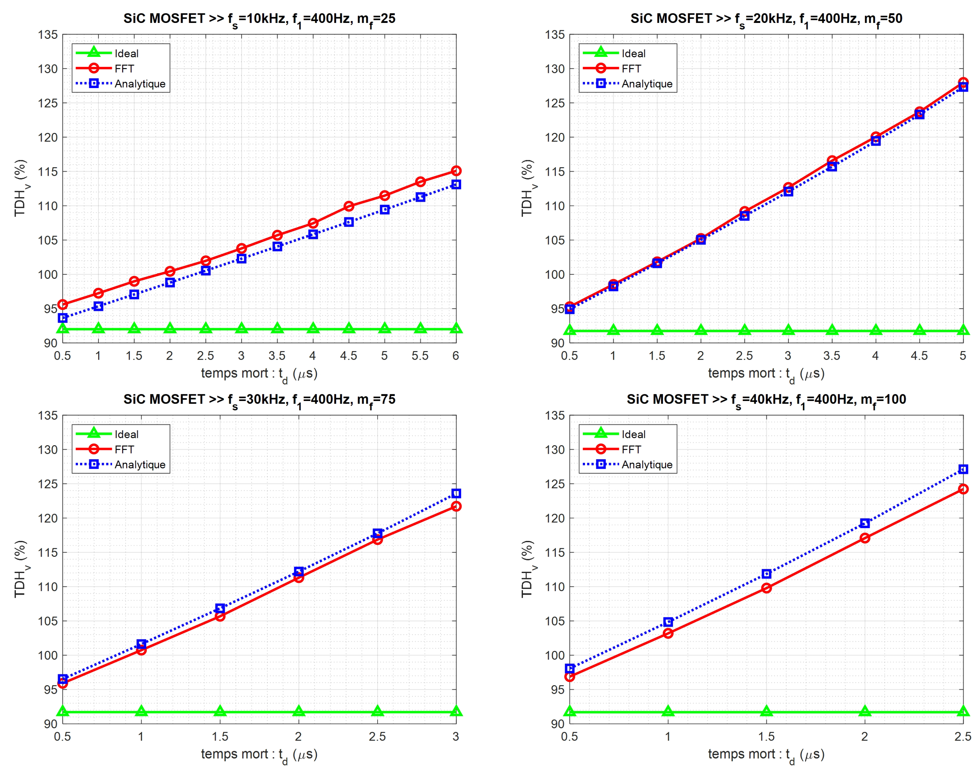
The decrease in the fundamental value with
, while the amplitudes of the different harmonics remain constant, leads to an increase in
with the PWM frequency for a given dead time. This observation is further supported by the
measurement results shown in
Figure 13. For instance, when comparing the
value for
, it increases from
at
to approximately
at
.
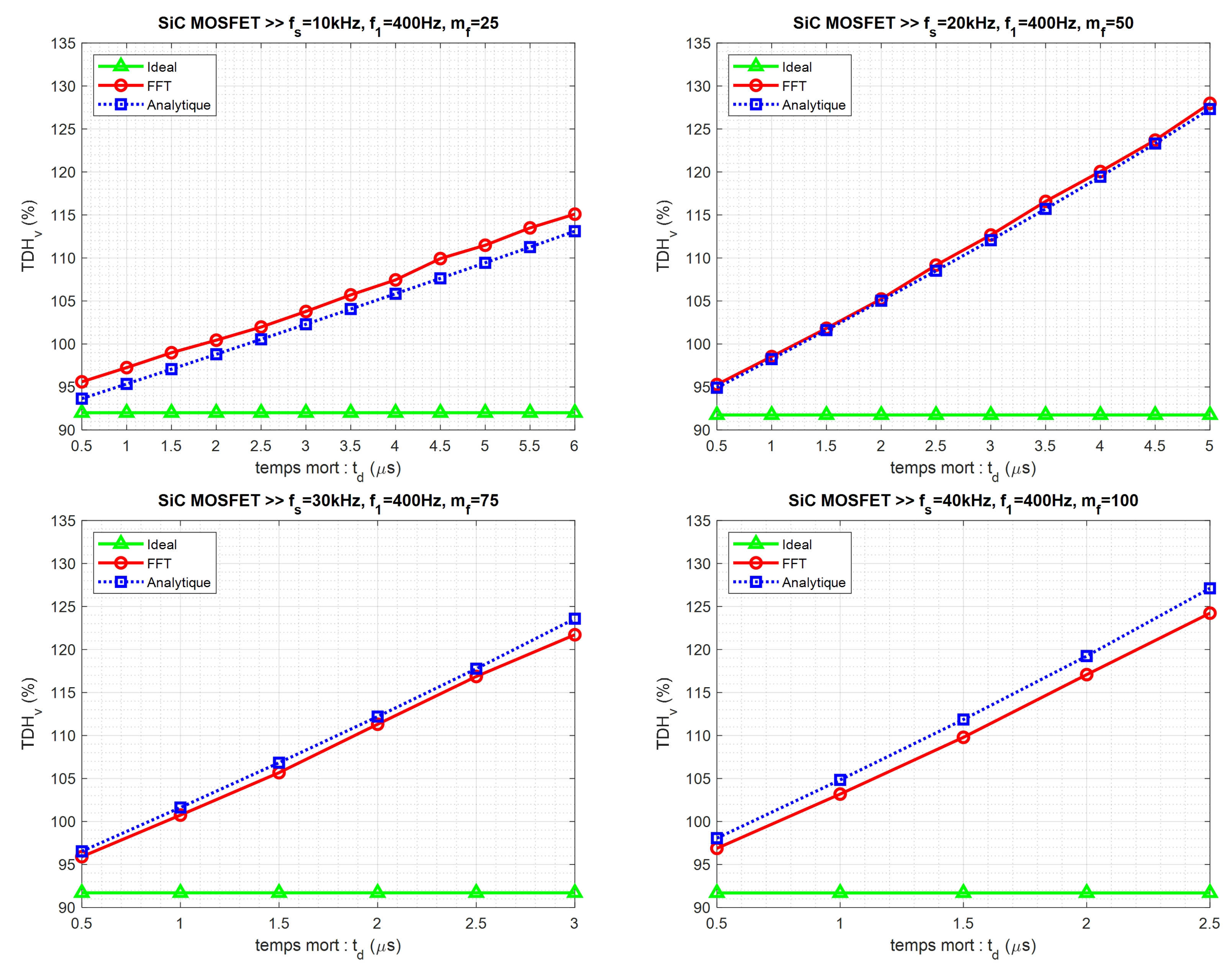
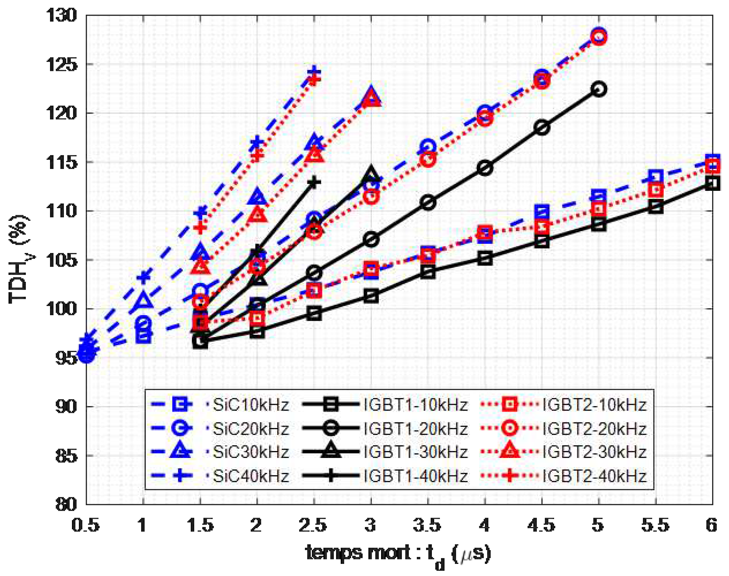
Figure 14 compares the measurement results of
for the 3 inverters under the same operating conditions. These results demonstrate that the
is consistently highest for the SiC-MOSFET inverter. However, selecting a very low dead time, which is possible with this type of component, can significantly improve
. We conducted a
measurement for the SiC-MOSFET inverter by setting the dead time to
. The results are shown in
Figure 14, indicating that the
remains at
regardless of the PWM frequency value.
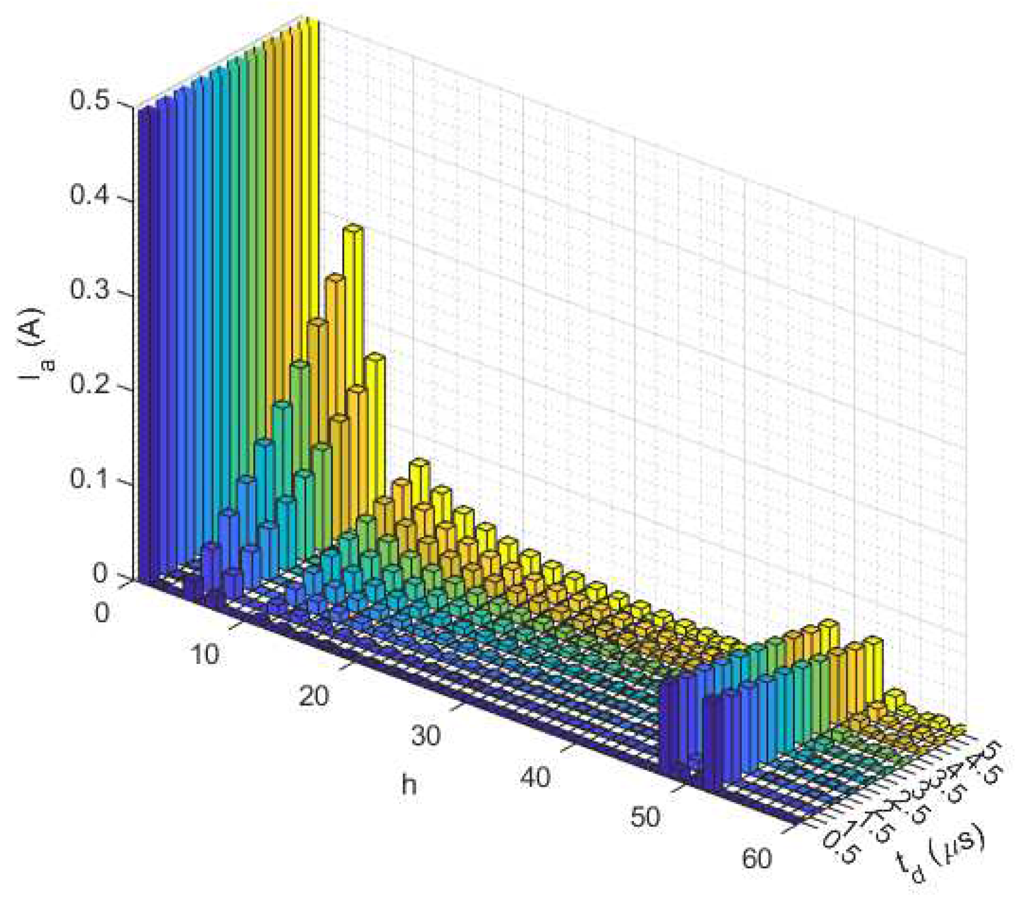
As mentioned earlier, low-frequency voltage harmonics (5
th, 7
th orders, etc.) arise due to dead times. While their impact on voltage remains relatively minor in comparison to PWM-induced harmonics, they gain significance in the current waveform due to the role of the R-L load as a low-pass filter. Various dead times (ranging from
to
) were tested on a SiC-MOSFET inverter operating with a 400 Hz fundamental frequency and 20 kHz PWM frequency (modulation factor,
).
Figure 15 illustrates the results with the fundamental current amplitude normalized to
A (the current value is
A). The increase in dead time amplifies the 5
th and 7
th order harmonics, overshadowing the PWM-related harmonics around the 50
th order. A near-linear correlation between the amplitude of the 5
th and 7
th harmonics and the dead time is evident from the findings in
Figure 15. The amplitude of the
-order harmonic (where
) for the current passing through the
load is governed by the following equation:
This relationship underscores the direct proportionality between
and the dead time value
, as corroborated by experimental observations. Applying Equation (
28) using the parameter values from Table 1 and adopting
and
mH, which corresponds to the experiments in
Figure 15, yields an
value of
A for
. This outcome closely aligns with the experimentally recorded value of approximately
A.
5. Conclusions
This paper introduces an analytical model for a three-phase inverter, encompassing factors such as dead times, switching times, voltage drops across components, and parasitic capacitance. The model effectively forecasts the voltage drop at the fundamental frequency of the inverter’s output voltage. Overlooking parasitic capacitance may result in an overestimation of this voltage drop. Among the contributors, dead times stand out as the primary cause of the most substantial voltage drop, influencing low-frequency harmonics that affect the load current.
The proposed model’s validity is established through experimental trials conducted on three-phase inverters equipped with distinct power components (IGBT and SiC MOSFET). The results demonstrate that the SiC inverter displays a greater voltage drop compared to IGBT-based inverters under identical dead time conditions. Nonetheless, the SiC inverter can significantly diminish the dead time to 0.5 µs, leading to a reduced voltage drop. The model consistently predicts the inverter’s output voltage drop and Total Harmonic Distortion (THD), with THD reduction at higher frequencies when minimizing dead time in the SiC-MOSFET inverter.
Furthermore, the impact of dead time on low-frequency harmonics is explored and verified through experimental tests, highlighting the significant influence of these harmonic amplitudes on THD. This emphasizes their role in shaping THD and underscores their importance in practical applications.
References
- Lin, Z.; An, Q.; Xie, C. SiC-Based Inverter Fed High-Speed Permanent Magnet Synchronous Motor Drive. 5th Asia Conference on Power and Electrical Engineering (ACPEE), 2020, pp. 1300–1304. [CrossRef]
- Allca-Pekarovic, A.; Kollmeyer, P.J.; Mahvelatishamsabadi, P. Comparison of IGBT and SiC Inverter Loss for 400V and 800V DC Bus Electric Vehicle Drivetrains. IEEE Energy Conversion Congress and Exposition (ECCE), 2020, pp. 6338–6344. [CrossRef]
- Perdikakis, W.; Scott, M.; Kitzmiller, C.; Yost, K.J. Comparison of Si and SiC EMI and Efficiency in a Two-level Aerospace Motor Drive Application. IEEE Transactions on Transportation Electrification, 1401. [Google Scholar] [CrossRef]
- Kapino, G.; Franke, W. Loss Comparison for Different Technologies of Semiconductors for Electrical Drive Motor Application. IEEE 13th International Conference on Compatibility, Power Electronics and Power Engineering (CPE-POWERENG), 2019. [CrossRef]
- Qi, F.; Wang, M.; Xu, L. Investigation and Review of Challenges in A High Temperature 30 kVA 3 phase inverter using SiC MOSFETs. IEEE Transactions on Industry Applications, 2483. [Google Scholar] [CrossRef]
- Shenoy, P.; Solis, O.; Zheng, L. Commercializing medium voltage VFD that utilizes high voltage SiC technology. IEEE International Workshop On Integrated Power Packaging (IWIPP), 2017. [CrossRef]
- Nawawi, A.; Tong, C.F.; Yin, S.; Sakanova, A. Design and Demonstration of High Power Density Inverter for Aircraft Applications. IEEE Transactions on Industry Applications, 1168. [Google Scholar] [CrossRef]
- Han, D.; Li, Y.; Sarlioglu, B. Analysis of SiC Based Power Electronic Inverters for High-Speed Machines. IEEE Applied Power Electronics Conference and Exposition (APEC), 2015, pp. 304–310. [CrossRef]
- Ding, X.; Du, M.; Duan, C.; Guo, H.; Xiong, R.; Xu, J.; Cheng, J.; Luk, P. Analytical and Experimental Evaluation of SiC-Inverter Nonlinearities for Traction Drives Used in Electric Vehicles. IEEE TRANSACTIONS ON VEHICULAR TECHNOLOGY. [CrossRef]
- Bedetti, N.; Calligaro, S.; Petrella, R. Self-Commissioning of Inverter Dead-Time Compensation by Multiple Linear Regression Based on a Physical Model. IEEE Applied Power Electronics Conference and Exposition - APEC 2014, 2015, 3954–3964. [Google Scholar]
- Bedetti, N.; Calligaro, S.; Petrella, R. Accurate modeling, compensation and self-commissioning of inverter voltage distortion for high-performance motor drives. IEEE Transactions on Industry Applications, 1550. [Google Scholar] [CrossRef]
- Dafang, W.; Peng, Z.; Yi, J.; Miaoran, W.; Gang, L.; Mingyu, W. Influences on Output Distortion in Voltage Source Inverter Caused by Power Devices’ Parasitic Capacitance. IEEE Transactions on Power Electronics, 4261. [Google Scholar] [CrossRef]
- Holmes, D.G.; Lipo, T.A. Modulation of Three-Phase Voltage Source Inverters. In Pulse Width Modulation for Power Converters: Principles and Practice; IEEE: New York City, NY, USA, 2003; pp. 215–258. [Google Scholar]
- Wu, C.M.; Lau, W.h.; Chung, H.S.h. Analytical Technique for Calculating the Output Harmonics of an H-Bridge Inverter with Dead Time. IEEE Transactions on Circuits and Systems I: Fundamental Theory and Applications 1999, 46, 617–627. [Google Scholar] [CrossRef]
- Deng, H.; Helle, L.; Bo, Y.; Larsen, K.B. A general solution for theoretical harmonic components of carrier-based PWM schemes. Proc. of the APEC 2009, 15-19 Feb. 2009, 2009, 1698–1703. [Google Scholar]
- Kus, V.; Josefova, T. The Influence of the Dead Time Duration and Switching Frequency on the Input Current Distortion of Voltage-Source Active Rectifiers. International Conference on Applied Electronics (AE) 2015, 08-09 September 2015, 2015, 1–4. [Google Scholar]
- Baghli, L.; Jamshidpour, E. Implementing a 200 kHz PWM Field Oriented Control using RTLib and C program on a dSPACE MicroLabBox. 2022 2nd International Conference on Advanced Electrical Engineering (ICAEE), 2022, pp. 1–6. [CrossRef]
Figure 1.
Three-phase Voltage Source Inverter.
Figure 1.
Three-phase Voltage Source Inverter.
Figure 2.
A-phase leg of three-phase inverter with the dead-time block.
Figure 2.
A-phase leg of three-phase inverter with the dead-time block.
Figure 3.
Waveform of the output voltage taking into account voltage drops, dead time, switching times and parasitic capacitors.
Figure 3.
Waveform of the output voltage taking into account voltage drops, dead time, switching times and parasitic capacitors.
Figure 4.
Effects of Parasitic Capacitance, (a) Switch turn on (b) switch turn off.
Figure 4.
Effects of Parasitic Capacitance, (a) Switch turn on (b) switch turn off.
Figure 5.
The average voltage drop due to parasitic capacitances as a function of is shown in the green curve, and the overall voltage drop (global voltage drop) is represented by the blue curve.
Figure 5.
The average voltage drop due to parasitic capacitances as a function of is shown in the green curve, and the overall voltage drop (global voltage drop) is represented by the blue curve.
Figure 6.
Effect of parasitic capacitance value on the output voltage drop.
Figure 6.
Effect of parasitic capacitance value on the output voltage drop.
Figure 7.
Experimental test bnch.
Figure 7.
Experimental test bnch.
Figure 8.
The voltage across a switch during the dead time is measured for different current levels and in the SiC-MOSFET inverter.
Figure 8.
The voltage across a switch during the dead time is measured for different current levels and in the SiC-MOSFET inverter.
Figure 9.
The voltage across a switch during the dead time is measured for different current levels and in the SiC-MOSFET inverter.
Figure 9.
The voltage across a switch during the dead time is measured for different current levels and in the SiC-MOSFET inverter.
Figure 10.
of (a) the SiC-MOSFET inverter, (b) the IGBT1 inverter, (c) the IGBT2 inverter.
Figure 10.
of (a) the SiC-MOSFET inverter, (b) the IGBT1 inverter, (c) the IGBT2 inverter.
Figure 11.
The voltage drop of the SiC inverter as a function of the PWM frequency for three different values of dead time.
Figure 11.
The voltage drop of the SiC inverter as a function of the PWM frequency for three different values of dead time.
Figure 12.
Comparison of the voltage drop for the 3 types of inverters.
Figure 12.
Comparison of the voltage drop for the 3 types of inverters.
Figure 13.
The variation of (Total Harmonic Distortion of voltage) for the SiC MOSFET inverter concerning dead time and at different modulation frequency indices .
Figure 13.
The variation of (Total Harmonic Distortion of voltage) for the SiC MOSFET inverter concerning dead time and at different modulation frequency indices .
Figure 14.
Comparison of the (Total Harmonic Distortion of voltage) for the SiC-MOSFET, IGBT1, and IGBT2 inverters, varying with dead time and at different PWM frequencies.
Figure 14.
Comparison of the (Total Harmonic Distortion of voltage) for the SiC-MOSFET, IGBT1, and IGBT2 inverters, varying with dead time and at different PWM frequencies.
Figure 15.
Experimental measurement of the current spectrum in the R-L load with modulation factor () for various dead time () values.
Figure 15.
Experimental measurement of the current spectrum in the R-L load with modulation factor () for various dead time () values.
Table 1.
Paramètres des composants.
Table 1.
Paramètres des composants.
| Paramètres |
IGBT1 |
IGBT2 |
SiC MOSFET |
| |
(SEMiX251GD126HD) |
(SKM100GB125DN) |
(CCS050M12CM) |
|
ou (V) |
1200 |
1200 |
1200 |
|
ou (A) à 25ºC |
242 |
100 |
87 |
|
(A) à 25ºC |
207 |
95 |
102 |
|
ou (m) |
7 |
22.5 |
25 |
|
(m) |
5 |
11.1 |
20 |
|
(V) |
0.9 |
2.3 |
0 |
|
(V) |
1.1 |
1 |
1.5 |
|
(mJ) |
37 |
11 |
1.1 |
|
(mJ) |
22 |
4 |
0.6 |
|
(mJ) |
12 |
4 |
- |
|
(ns) |
295 |
75 |
51 |
|
(ns) |
625 |
600 |
69 |
|
() |
10 |
10 |
20 |
Table 2.
Specifications of the three-phase inverter.
Table 2.
Specifications of the three-phase inverter.
| Parameters |
Value |
| DC bus voltage () |
V |
| Output current of the inverter () |
30 Arms |
| PWM frequency () |
10-100 kHz |
| Fundamental frequency () |
50-3000 Hz |
| Efficiency () |
|
|
Disclaimer/Publisher’s Note: The statements, opinions and data contained in all publications are solely those of the individual author(s) and contributor(s) and not of MDPI and/or the editor(s). MDPI and/or the editor(s) disclaim responsibility for any injury to people or property resulting from any ideas, methods, instructions or products referred to in the content. |
© 2020 by the authors. Licensee MDPI, Basel, Switzerland. This article is an open access article distributed under the terms and conditions of the Creative Commons Attribution (CC BY) license (https://creativecommons.org/licenses/by/4.0/).
