
Submitted:
15 August 2023
Posted:
18 August 2023
You are already at the latest version
Abstract
Edge computing has emerged as a significant computing trend alongside the rapid expansion of the Internet of Things (IoT). Computing operations at the network’s edge offer a solution to the high latency and service overload challenges often associated with cloud computing. Additionally, the Secure Hash Algorithm-3 (SHA-3) plays a crucial role in ensuring data integrity and is implemented for numerous applications in the IoT field. Therefore, integrating the SHA-3 accelerator into edge computing is essential. Moreover, recent studies about SHA-3 have primarily focused on achieving high performance and optimizing resource utilization for SHA-3. However, these studies have overlooked the crucial aspect of data transfer between the external memory and the hash function block, as transfer time plays a significant role. This paper proposes an efficient SHA-3 architecture designed for System-on-Chip (SoC) Field Programmable Gate Array (FPGA) to address the aforementioned challenges and be suitable for real edge computing. The architecture contains three key techniques. First, the harmony of padding and Direct Memory Access (DMA) for managing the data transfer process and enhancing performance efficiency based on Serial Input to Parallel Output (SIPO) and a barrel shifter. Secondly, implementing internal pipelining within the Round Function (RF) to reduce critical path delays and optimize resource utilization. Finally, designing four modes (SHA3-224, SHA3-256, SHA3-384, and SHA3-512) to cater to various applications. Our architecture is implemented and tested on the DE10-Standard Development Kit (Cyclone V SX SoC-5CSXFC6D6F31C6N), which is integrated into the FPGA and is controlled by a Dual-Core ARM Cortex-A9 processor. The result is up to 38.34 Gbps in throughput and 5.61 Mbps/ALM in efficiency for the RF computation, 28.02 Gbps in throughput, and 3.63 Mbps/ALM for the full proposed architecture.
Keywords:
SHA-3 accelerator
; Edge computing
; Padding
; Round function
; SoC FPGA
1. Introduction
SHA-3 has emerged as a new-generation hash function, replacing older algorithms due to their vulnerabilities [1]. It has widespread adoption in modern applications for ensuring security and integrity, including digital signatures, pseudorandom bit generation, and message authentication codes. Concurrently, with the rapid advancement of IoT, the number of IoT devices has increased significantly, opening the period of edge computing [2]. This paradigm offers several advantages in networks, such as low latency, reduced bandwidth consumption... However, to exploit these benefits, edge computing must handle the hash computation demands from the variety of IoT devices. Therefore, the need for an SHA-3 accelerator with high performance and flexibility to process hash computations from diverse hash functions of IoT devices is evident for edge computing. Consequently, a significant percentage of recent research has been concentrated on designing high-speed and efficient SHA-3 hardware, driven by the aforementioned factors.
To achieve efficiency, it is essential to consider both performance and resource utilization. Numerous studies have explored two methods to address this challenge: enhancing throughput and optimizing resource usage. In terms of reducing resource requirements, most previous researchers have focused on the datapath. Instead of using the full 1600 bits datapath, they have considered a lower-bit one. For example, authors of [3,4,5] adopted a folding structure and applied a slice-oriented strategy, and selected a 25, 200, and 400 bits internal path, respectively. In the study [3,4], changing the order of sub-functions resulted in an increased number of rounds, specifically which pluses one round compared to a standard number of rounds. Similarly, the authors of [5] arranged the order of sub-functions such as rho, pi, chi, iota, and theta. While these aforementioned studies achieved notable gains almost optimized resources significantly, the architectures employed still exhibited low performance. Several high-performance techniques are employed to address the high-performance requirements of SHA-3 architectures. These techniques include pipelining, unrolling, and leveraging existing resources available on FPGA. In the study [6,7], pipeline registers are inserted after each RF, increasing the throughput without impacting the number of rounds in the architecture. Another approach discussed in [8] focuses on enhancing throughput by reducing the number of rounds. This is achieved by combining two adjacent rounds, effectively reducing 24 to 12 rounds. Additionally, a pipeline technique is applied within the RF. This approach, proposed by the authors in [9,10], involves the insertion of registers between the pi and chi functions to reduce critical path delays. In addition to improving performance, the designs in [8,10] also exhibit a high level of flexibility, enabling support for applications with multiple modes of SHA-3.
Most of the aforementioned studies primarily focus on addressing challenges within the RF of the SHA-3 accelerator. However, it is important to consider that the overall processing time consists of computing and transfer time. Simply optimizing the computing time without addressing the transfer time can result in a bottleneck for the entire SHA-3 accelerator. In order to maintain the SHA-3 accelerator operating at a high rate, it is crucial to make a continuous and compatible flow of required data. Additionally, the storage resources of the accelerator are limited, which means they can only accommodate the necessary data for one or a few computations. For the SHA-3 accelerator to be truly efficient, it must effectively resolve high-speed computation and efficient and appropriate data transfer. By addressing both aspects, we can maximize the overall performance and effectiveness of the SHA-3 accelerator.
In this paper, we aim to enhance the computation and data transfer performance and versatility of the SHA-3 accelerator. Three factors help us gain this target. Firstly, the harmony of padding and DMA. Padding, the first phase of the SHA-3 algorithm, is the place receiving data and extending data to satisfy the input condition. The data transfer process is sequential, and the datapath size impacts the padding rate. Therefore, we design sequential padding suitable for the basic transfer mechanism with a large datapath. Furthermore, we adopt a proactive approach to retrieve data from external memory to eliminate any idle time within the SHA-3 accelerator and fully utilize available resources. DMA proves to be an ideal technique for this purpose, as it allows the SHA-3 accelerator to directly access memory without passing through intermediate caches such as L2 and L3. This enhances the efficiency of data retrieval and reduces the memory access path, resulting in improved overall performance. Secondly, an internal pipeline within the RF. The RF comprises five key sub-functions, which can introduce a long critical path and consequently decrease the overall speed of the SHA-3 implementation. To shorten this, we insert pipeline registers at the beginning and end of the theta sub-function, effectively dividing the RF into two stages. Additionally, we enable one RF to process two message blocks simultaneously to maximize resource utilization. This optimization helps reduce the critical path and improve the overall performance of the SHA-3 accelerator. Finally, designing the SHA-3 with multiple modes that share a common sponge structure. The differences between the modes primarily lie in the input and output steps, which can be easily implemented using a multiplexer. By developing multiple modes, our SHA-3 implementation can adapt to various scenarios, providing flexible hashing capabilities while maintaining efficiency.
2. Background SHA-3 algorithm
The SHA-3 hash functions are derived from the KECCAK function, where the message is appended with a two bits suffix, specifically "01". To provide varying digest lengths, the SHA-3 family offers four hash functions: SHA3-224, SHA3-256, SHA3-384, and SHA3-512. The distinction between these functions relies on several parameters. One such parameter is the rate, denoted as r, which indicates the block size and is dependent on the length of the message. The capacity, denoted as c, is determined by the equation , where b represents the internal width. The output length, denoted as d, is also derived from . These parameters are summarized in Table 1.
The differences between the SHA-3 modes result in slight variations in the padding operation and truncation step. However, the modes operate in a similar manner for other steps. The pseudocode for the SHA-3 family is presented in Algorithm 1. It consists of three main parts: padding, absorbing, and squeezing.
| Algorithm 1:SHA-3 hash functions. |
|
1.15
SPONGE: InputM: input message OutputZ: hash value
|
2.1. Padding
A padding process is performed to align the length of the input message with the requirements of the hash function algorithm. This process involves appending the format "10*1" to the original message, resulting in a new message length that is a multiple of the bitrate r. Specifically, the primitive message M is extended by adding "01" to create a new message N. Following that, a "1" bit, followed by j bits of "0" and a final "1" bit, is added at the end. The total length of the padded message has to satisfy the condition , where n is an integer number. After the padding process, the padded message is divided into n blocks, each with a size of r.
2.2. Absorbing
Once the padded message is divided into r bit blocks (), where i ranges from 0 to , each block is extended by appending c zero bits. The extended blocks are then XORed with the state array S. The permutation process involves applying the RF and repeating it 24 times. The RF follows a specific order of sub-functions: theta, rho, pi, chi, and iota. These sub-functions utilize logic gates like AND, XOR, shift, and rotate, which are well-suited for hardware implementation.
2.3. Squeezing
The SHA-3 hash function produces digest values of varying fixed lengths determined by the specific mode. For example, SHA3-224 generates a 224-bit digest, SHA3-256 produces a 256-bit digest, SHA3-384 yields a 384-bit digest, and SHA3-512 generates a 512-bit digest.
3. The proposed SHA-3 architecture
3.1. System-level overview and features
The proposed SHA-3 accelerator system is depicted in Figure 1, which consists of two main parts: the master component of Central Processing Unit (CPU), ARM Cortex-A9, and the slave component of SHA-3 accelerator. The CPU plays a central role in controlling most of the components within the system and is constantly engaged in managing multiple processes. Given the CPU’s heavy workload, it becomes difficult to immediately provide data to the SHA-3 accelerator, resulting in delays. To overcome this limitation, the SHA-3 accelerator takes a proactive approach by independently retrieving data from the external memory; specifically, the Synchronous Dynamic Random Access Memory (SDRAM). This proactive data retrieval helps minimize waiting times and ensures a continuous data flow for the accelerator’s operations. Moreover, when the CPU needs to provide data to various components, it follows a process that involves retrieving data from memory and passing it through intermediate components, such as the L3 interconnect, before reaching the intended destination. As a result, the datapath becomes longer, potentially impacting overall performance. To address this, the DMA technique (Read DMA and Write DMA) is employed within the SHA-3 accelerator to reduce the long datapath for accessing the SDRAM and optimize data transfer times. This approach enhances the efficiency and speed of data retrieval for the SHA-3 accelerator, contributing to improved system performance.
In the SHA-3 accelerator (as shown in Figure 1), there are three main components: the padding block, multiple RFs, and the Parallel Input Serial Output (PISO) block. The padding block is designed to match the size of the input to the DMA’s datapath, maximizing the utilization of the supported datapath and reducing the padding time. This optimization leads to a significant increase in the padding rate. The three RFs chosen for this design serve two primary purposes. Firstly, since the hash computation requires 24 loops for one digest, having three RFs results in an average period of input data being eight clock cycles. Secondly, in the case of SHA3-224, with the longest input length of 1152 bits, the padding time is approximately 256 times 5 (256 is the size of the padding’s input datapath), and another overhead cost makes the padding time greater than five clock cycles. Therefore, having three RFs allows for efficient processing. Furthermore, each RF includes two pipeline stages, contributing to the higher frequency and improved throughput. Additionally, these two pipeline stages enable the simultaneous computation of two messages, further enhancing the performance and efficiency of the SHA-3 accelerator. The PISO block transfers the hash value to one or more 256-size data.
The system’s working flow involves two main phases. Firstly, the data preparation phase takes place at the SDRAM. Here, the required data is stored and organized in the memory to be ready for processing by the SHA-3 accelerator. Secondly, the CPU sends the configuration settings to the config block of the SHA-3 accelerator through a lightweight bridge. The SHA-3 accelerator utilizes the parameters provided in the config block to determine essential information, such as the read address, write address, message length, and selected modes. These parameters enable the proposed accelerator to actively load and store data into the SDRAM relying on Read DMA and Write DMA, respectively. As shown in Figure 2, once the config block receives the config 0 package, the requirement to read data from DMA is sent immediately. The padding block receives message 0 and feeds it to one of the RFs. This process is repeated for message 1, message 2, and so on, up to a maximum of six messages, as the proposed SHA-3 accelerator can handle six messages simultaneously. Once a hash value is generated, the Write DMA stores it in SDRAM. Additionally, the config block can continuously receive requirements from the CPU, executing each requirement immediately as soon as the padding is available. Therefore, the system can achieve parallel processing thanks to the proactiveness of loading and storing data. Input data transfer, hash value computation, and output data transfer are executed simultaneously. This parallel execution optimizes the system’s performance, enabling efficient and high-speed data processing by the SHA-3 accelerator.
3.2. The proposed padding architecture
In our architecture as Figure 3, the padding block serves three primary functions: SIPO, selecting SHA-3 type (using a multiplexer), and a barrel shifter. The SIPO component receives data from the Read DMA, and once five data chunks are accumulated, they are passed to the multiplexer. The multiplexer adjusts the amount of data bits according to the specific SHA-3 mode being used. For instance, SHA3-224 requires 1152 bits of data and 448 bits of zeros; SHA3-256 requires 1088 bits of data and 512 bits of zeros; SHA3-384 requires 832 bits of data and 768 bits of zeros; SHA3-512 requires 576 bits of data and 1024 bits of zeros. This architecture enables straightforward switching between different SHA-3 modes during data transfer. The barrel shifter is implemented in parallel with SIPO and the multiplexer. Finally, the outputs of SIPO, multiplexer, and the barrel shifter are ORed together to generate the padding result.
We employ five consecutive buffers to receive data from the Read DMA. The choice of five buffers is based on two considerations. Firstly, each buffer is sized to match the datapath size of 256 bits. Secondly, the longest input data length in the SHA3-224 case is 1152 bits. By allowing flexibility in the number of buffers based on the datapath size before synthesis on FPGA, we aim to optimize efficiency and enhance performance. The input data for the SIPO can consist of either 256-bit data from the Read DMA or 256-bit zeros, depending on the length of the data. The length block contains the data length, converted to a 256-based length to determine the number of received data. Once the SIPO has received the required data, any remaining input data is filled with zeros. For example, in Figure 4, if the length is 600 bits, the 256-based length is rounded to 3. This means that the SIPO will receive three input data from the Read DMA and two 256-bit zeros.
Figure 5 depicts the padding construction process, which involves extending the data with a 4-bit sequence "0110" after the data length t and always placing a "1" bit at the position. Thus, we split this process into two parts. In the first part, the "1" value at the position is set using a multiplexer, as illustrated in Figure 3. Specifically, once the SIPO has received sufficient data, the data is truncated based on the input length r of the specific mode (as defined in Table 1), and the "1" bit is placed at the position. In the second part, the 4-bit sequence "0110" is appended to the data using the barrel shifter technique, as shown in Figure 3. The barrel shifter consists of ten multiplexer layers, allowing a maximum data length of 11 bits. Finally, the resulting padded data is obtained by XORing the output of the two aforementioned parts.
3.3. The internal pipelined RF
The RF depicted in Figure 6 is divided into two pipelined stages within RF, which takes place inside one loop so that this RF is reused 24 times to generate the digest, called the internal pipeline. The first stage focuses only on the theta sub-function, the most time-consuming sub-function. According to Algorithm 1, the theta sub-function requires at least three levels to complete: computing variable C from the input data including five XOR operations, computing variable D from the previous result C including one XOR operation, and obtaining the theta’s result based on variable D which one XOR implements. The second stage contains the rho, pi, chi, and iota sub-functions.
The rho sub-function is precomputed and directly assigned to the appropriate destination. Specifically, to simplify rho, we parameterize it using a left rotation on the dimension z with a fixed coefficient (as shown in Table 2) following eq. 1, where is the left rotation, N is the shifting coefficient, , and .
The pi sub-function is responsible for rearranging the positions of the lanes. However, directly implementing this formula in hardware may not be the most efficient approach. To optimize the process, we precompute the swap positions of the lanes and assign them directly to the desired locations. The resulting swapped positions are conveniently presented in Table 3.
The chi sub-function involves a delay of AND, XOR, and NOT operations which do not introduce significant delays. Finally, the iota sub-function is simplified by XORing certain bit positions with the Round Constant (RC). In our design, this information is precomputed and stored in a 7-bit format, as illustrated in Table 4.
In this architecture, the RF can compute two data parallelly due to two pipelined stages. Each data requires 24 loops to complete, as each loop is divided into two stages. Thus, it takes 48 clocks to process each piece of data. As depicted in Figure 7, when the first input is introduced to the RF, a counter is employed to keep track of the number of loops. After every two clocks, the counter increments until it reaches a value of 23. Furthermore, the second input can be inserted into the RF at any time, indicated by the variable t in Figure 7. This variable can have a value greater than zero, implying that the second input can be introduced one or more clocks after the first input. This flexibility allows the RF to operate efficiently in handling multiple inputs as well as always leverage 100% of the RF resource.
4. Evaluation and Result
In the performance evaluation, we conducted two parts. Firstly, we evaluated the computation of the RF in our proposed architecture (multiple RFs), comparing it to related approaches. The RF is a critical component of the SHA-3 algorithm, and previous researchers have done significant optimizations. In the second part, we compared the complete architecture, including padding, RF, and other supporting components like SIPO and POSI, with previous studies that may have some or all of these components. The comprehensive results of these two parts are summarized in Table 5 and Table 6.
For our proposed architecture, we performed synthesis using Quartus Prime Lite Edition version 21.1 on the Cyclone V SX SoC-5CSXFC6D6F31C6N. The ThroughPut (TP) was calculated using eq. (2),where the number of input bits (#bit), the maximum frequency (Fmax) obtained from synthesis, and the average number of clock cycles (#Clock) required for hash value generation (known as #Clock/Hash). To evaluate the efficiency, we used eq. (3), comparing throughput with resource utilization. The design’s area was measured, and since Intel and Xilinx devices have different components, we compared the Adaptive Logic Module (ALM) of Intel’s Cyclone V (CV) device with the Slice of Xilinx’s Virtex 5 (V5) and Virtex 6 (V6) devices.
The proposed architecture, incorporating multiple RFs, achieves Fmax of 266.24 MHz utilizing 6837 ALMs. The corresponding throughput values for SHA3-224, SHA3-256, SHA3-384, and SHA3-512 are 38.34 Gbps, 36.31 Gbps, 27.69 Gbps, and 19.17 Gbps, respectively. Furthermore, the efficiency is measured at 5.61 Mbps/ALM, 5.30 Mbps/ALM, 4.05 Mbps/ALM, and 2.80 Mbps/ALM for SHA3-224, SHA3-256, SHA3-384, and SHA3-512, respectively. Our proposed architecture demonstrates 2.58 times higher throughput than [11] while achieving 0.47 times higher efficiency than [11] in SHA3-256 mode. Moreover, the proposed multiple RFs are 1.60 times than [12] in throughput, and 0.33 times than [12] in efficiency for SHA3-256.
In the full proposed architecture, we obtain Fmax of 194.50 MHz, utilize 7702 ALMs, achieve the throughput of 28.02 Gbps, 26.46 Gbps, 20.24 Gbps, and 14.01 Gpbs and the efficiency of 3.63 Mbps/ALM, 3.43 Mbps/ALM, 2.62 Mbps/ALM, and 1.82 Mbps/ALM for SHA3-224, SHA3-256, SHA3-384, and SHA3-512, respectively. Compared to [9], we achieve 1.11 times in throughput and 0.67 times in efficiency for SHA3-512. Compared to [13], we achieve 1.86 times in throughput and 0.32 times in efficiency for SHA3-512 mode. Furthermore, our full design obtains approximately 1.17 times than [8] in the throughput and about 1.89 times than [8] in the efficiency for all modes.
In Table 5, the #Clock/Load represents the number of clocks required to load data from external memory. For SHA3-224, SHA3-256, SHA3-384, and SHA3-512, we achieved load times of 5, 5, 4, and 3 clocks, respectively. These values are lower than the #Clock/Hash (8 clocks), indicating that the SHA-3 accelerator effectively avoids any potential bottlenecks.
5. Conclusion
In this paper, we emphasized the importance of addressing both the computation time and transfer time in SHA-3 accelerators, high-performance hash computation, and the need for flexibility to adapt to different scenarios in edge computing. We applied three factors to solve these challenges: the harmony of the padding and DMA, the internal pipeline inside the RF, and the supported multiple modes. Regarding performance, we analyzed the achieved throughput values for different SHA-3 modes. The proposed architecture demonstrated impressive results on the Cyclone V device, with throughput values of 38.34 Gbps for the RF and 28.02 Gbps for the full proposed architecture. Additionally, we evaluated the device utilization in terms of ALMs. The proposed architecture effectively utilized 6837 ALMs for the multiple RFs, while the full proposed architecture utilized 7702 ALMs. These values signify significant improvements compared to previous studies and highlight the enhanced computational capabilities of our design.
Author Contributions
Conceptualization, supervision, and validation, H.-T.H; methodology and software, T.-K.T; review and editing, T.-T.H; review, C.-K.P; research, proposal, and implement, T.-P.D. All authors have read and agreed to the published version of the manuscript.
Funding
This research is funded by the University of Science, VNU-HCM, under grant number ÐT-VT 2022-03.
Institutional Review Board Statement
Not applicable.
Informed Consent Statement
Not applicable.
Data Availability Statement
Data are contained within the article.
Conflicts of Interest
The authors declare no conflict of interest.
References
- Federal Information Processing Standards Publication. SHA-3 Standard: Permutation-Based Hash and Extendable-Output Functions, Aug. 2015. [CrossRef]
- Cao, Keyan and Liu, Yefan and Meng, Gongjie and Sun, Qimeng. An Overview on Edge Computing Research. IEEE Access 2020, 8, 85714–85728. [CrossRef]
- Jungk and M. Stöttinger. Serialized Lightweight SHA-3 FPGA Implementations. Microprocessors and Microsystems Nov. 2019, 71, 102857. [CrossRef]
- B. Jungk and J. Apfelbeck. Area-Efficient FPGA Implementations of the SHA-3 Finalists. Int. Conf. on Reconfigurable Comp. and FPGAs, Nov. 2011, pp. 235–241. [CrossRef]
- M. Sundal and R. Chaves. Efficient FPGA Implementation of the SHA-3 Hash Function. IEEE Computer Society Annual Symp. on VLSI (ISVLSI), Jul. 2017, pp. 86–91. [CrossRef]
- H. E. Michail, L. Ioannou, and A. G. Voyiatzis. Pipelined SHA-3 Implementations on FPGA: Architecture and Performance Analysis. Workshop on Crypto. and Secu. in Comp. Syst., 2015, p. 13–18. [CrossRef]
- M. M. Wong, J. H.-Yahya, S. Sau, and A. Chattopadhyay. A New High Throughput and Area Efficient SHA-3 Implementation. IEEE Int. Symp. on Circ. and Syst. (ISCAS), 18, pp. 1–5. 20 May. [CrossRef]
- S. El Moumni, M. Fettach, and A. Tragha. High throughput implementation of SHA3 hash algorithm on field programmable gate array (FPGA). Microelectronics Journal Nov. 2019, 93, 104615. [CrossRef]
- H. Mestiri, F. Kahri, M. Bedoui, B. Bouallegue, and M. Machhout. High Throughput Pipelined Hardware Implementation of the KECCAK Hash Function. Int. Symp. on Signal, Image, Video and Comm. (ISIVC), Nov. 2016, pp. 282–286. [CrossRef]
- G. S. Athanasiou, G.-P. Makkas, and G. Theodoridis. High Throughput Pipelined FPGA Implementation of the New SHA-3 Cryptographic Hash Algorithm. Int. Symp. on Comm., Control and Signal Processing (ISCCSP), May 2014, pp. 538–541. 20 May. [CrossRef]
- P. Gangwar, N. Pandey, and R. Pandey. Novel Control Unit Design for a High-Speed SHA-3 Architecture. IEEE Int. Midwest Symp. on Circ. and Syst. (MWSCAS), Aug. 2019, pp. 904–907. [CrossRef]
- A. Sideris, T. Sanida, and M. Dasygenis. High Throughput Pipelined Implementation of the SHA-3 Cryptoprocessor. Int. Conf. on Microelec. (ICM), Dec. 2020, pp. 1–4. [CrossRef]
- F. Assad, F. Elotmani, M. Fettach, and A. Tragha. An Optimal Hardware Implementation of the KECCAK Hash Function on Virtex-5 FPGA. Int. Conf. on Syst. of Collaboration Big Data, Internet of Things & Secu. (SysCoBIoTS), Dec. 2019, pp. 1–5. [CrossRef]
Figure 1.
The overview of the proposed SHA-3 architecture at system level on Cyclone V.
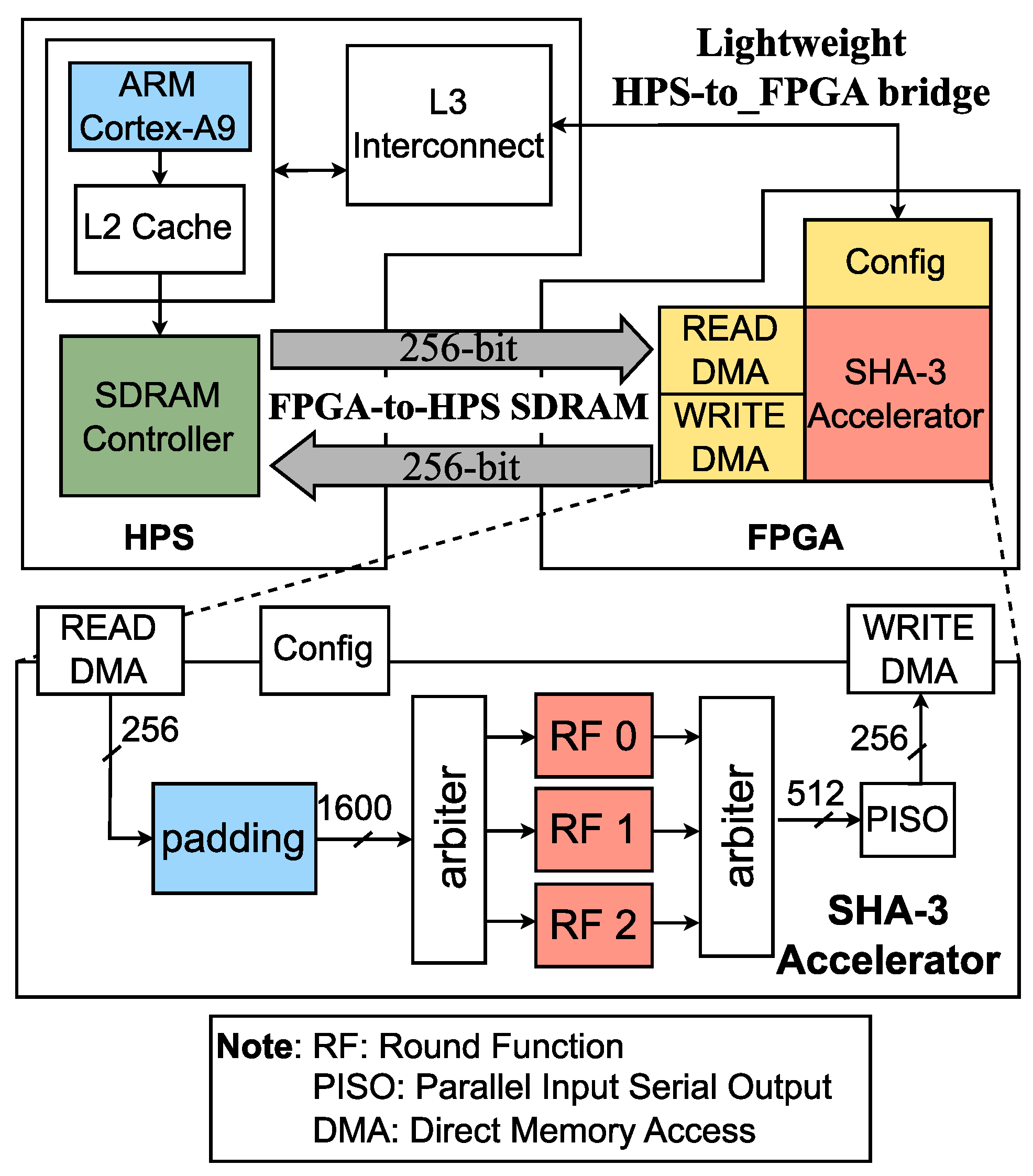
Figure 2.
The timing chart of the proposed SHA-3 at the system level.
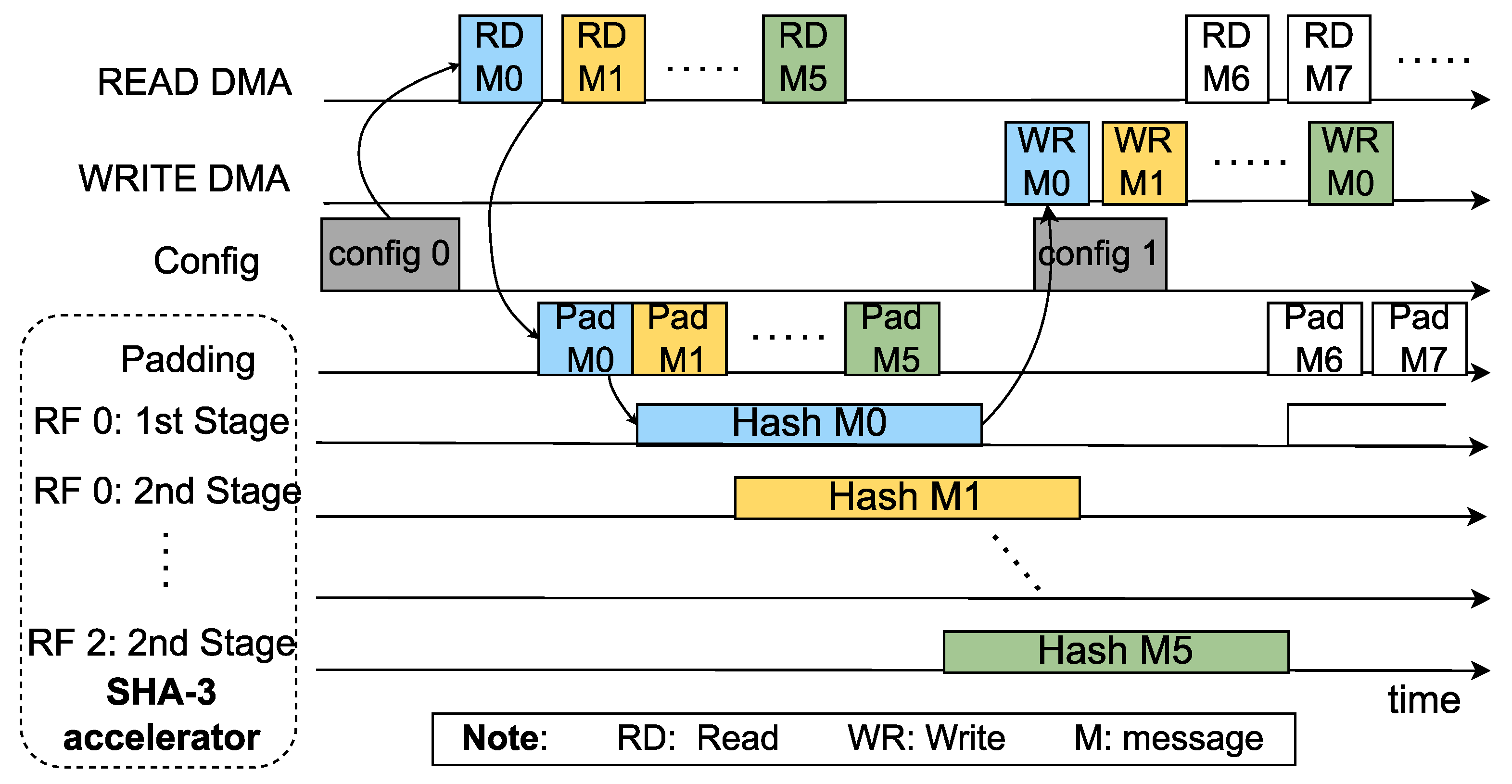
Figure 3.
The proposed padding architecture.
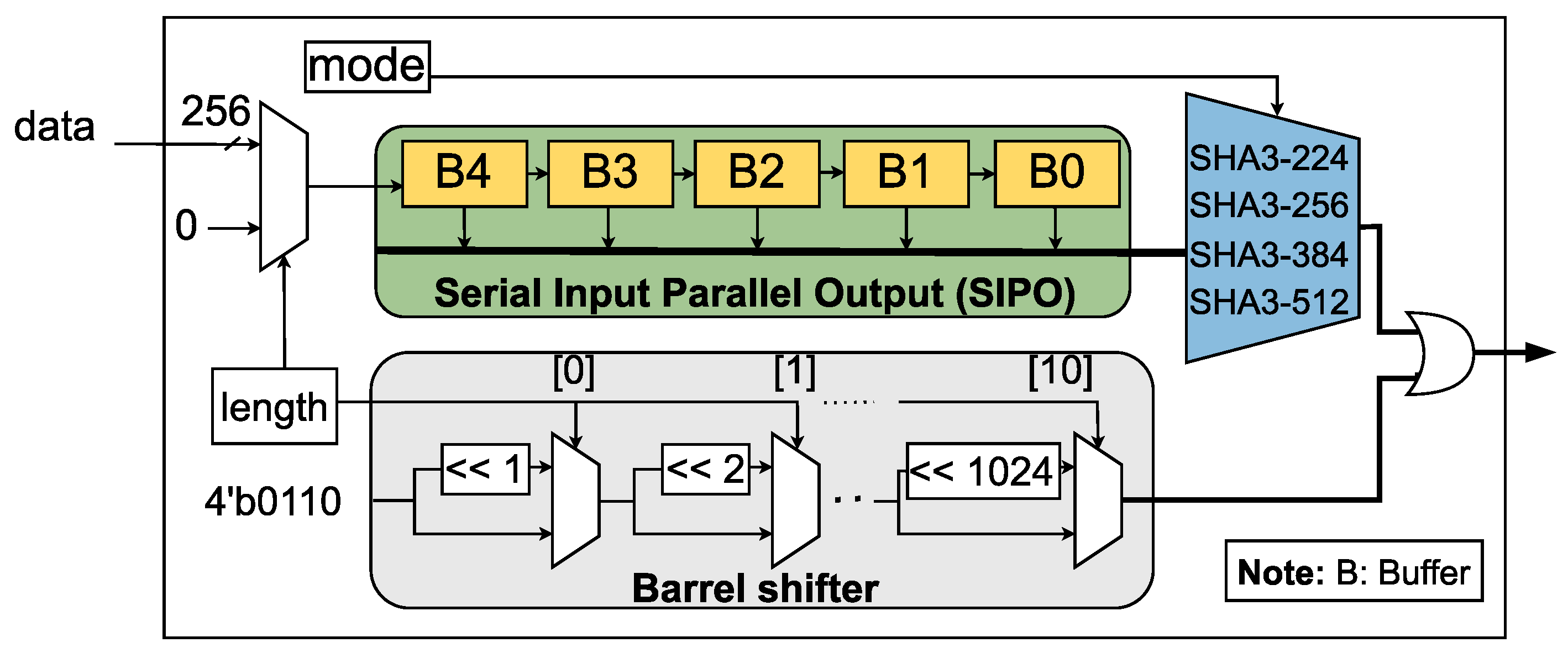
Figure 4.
The timing chart of SIPO.
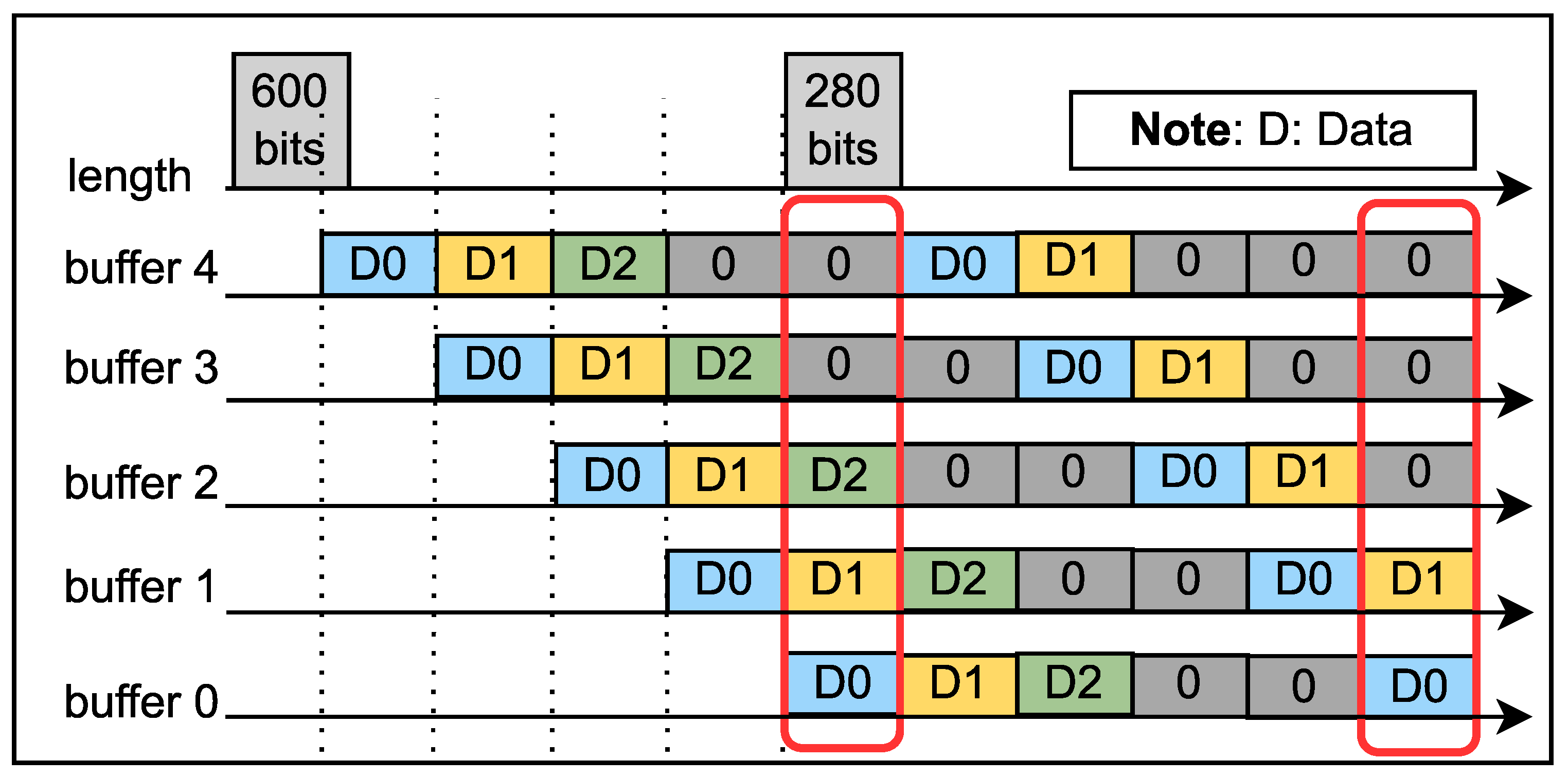
Figure 5.
The construction of the padded message.
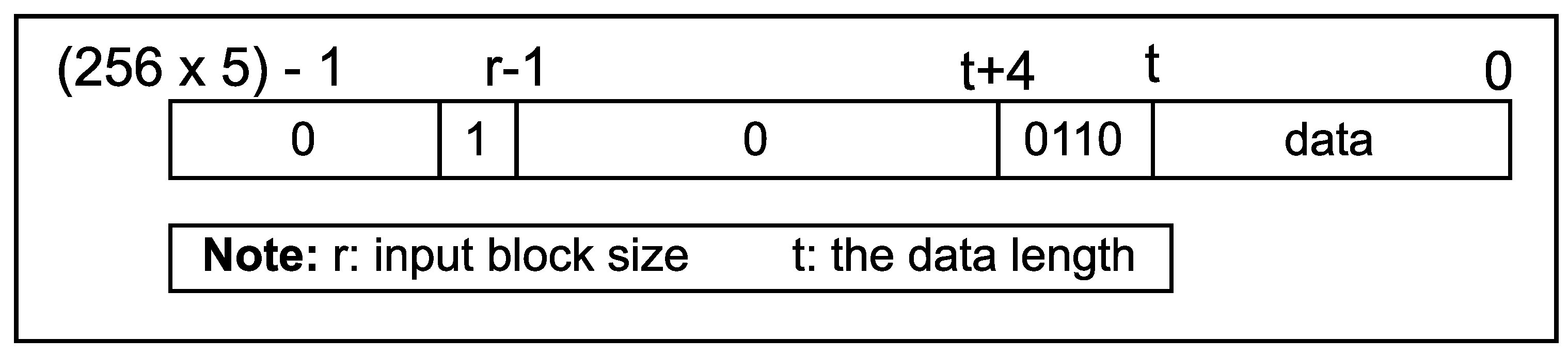
Figure 6.
The internal pipelined RF architecture.
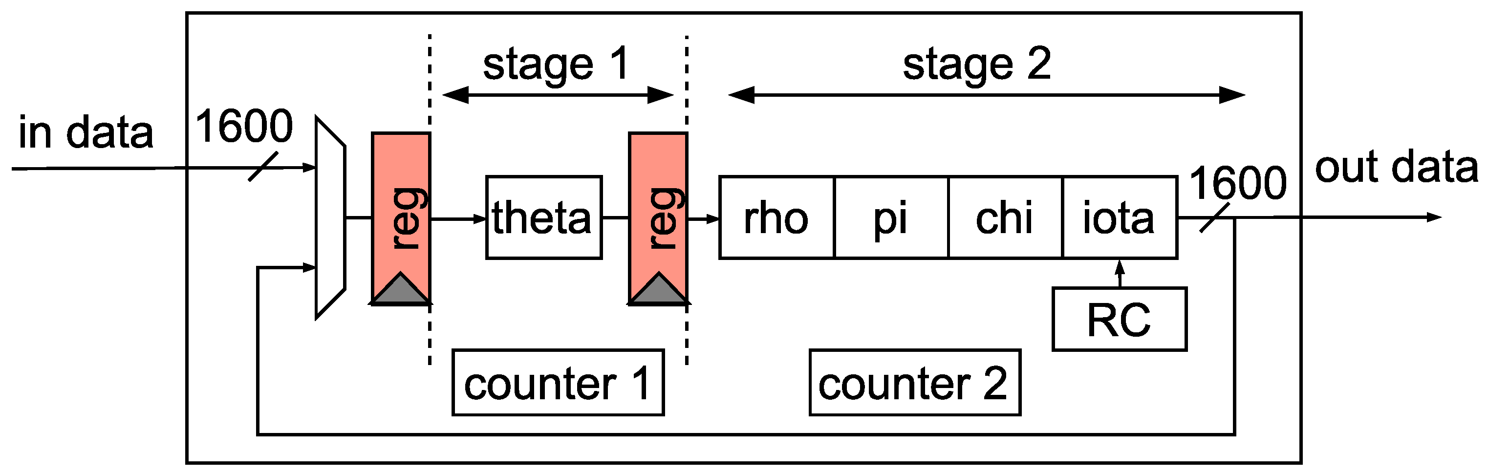
Figure 7.
The timing chart of the RF.
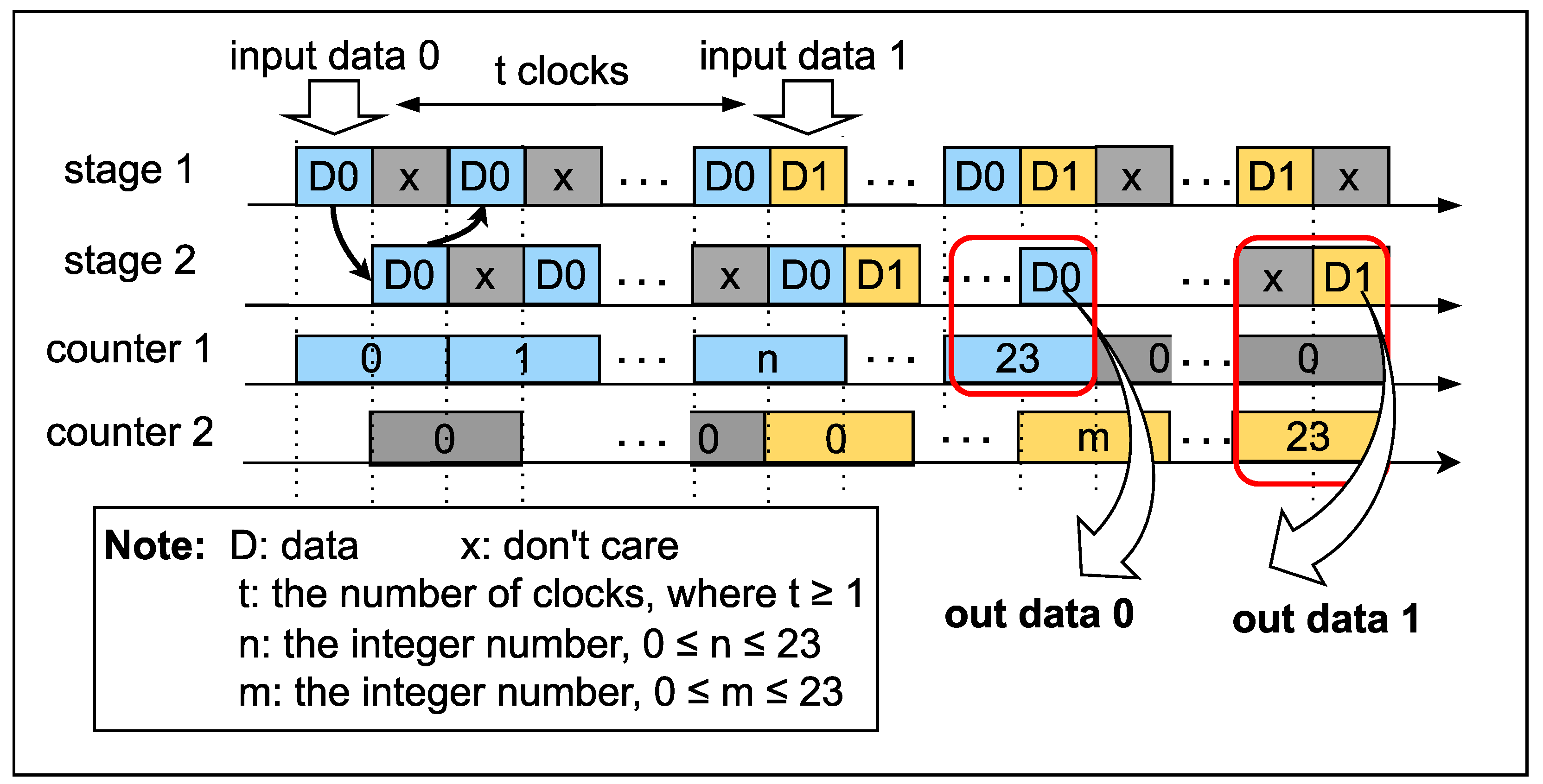

Table 1.
The parameters of the SHA-3 modes.
| Mode | SHA3-224 | SHA3-256 | SHA3-384 | SHA3-512 |
|---|---|---|---|---|
| b (bit) | 1600 | 1600 | 1600 | 1600 |
| r (bit) | 1152 | 1088 | 832 | 576 |
| c (bit) | 448 | 512 | 768 | 1024 |
| d (bit) | 224 | 256 | 384 | 512 |
Table 2.
The shifting coefficient of rho sub-function.
| 0 | 1 | 62 | 28 | 27 | |
|---|---|---|---|---|---|
| 36 | 44 | 6 | 55 | 20 | |
| 3 | 10 | 43 | 25 | 39 | |
| 41 | 45 | 15 | 21 | 8 | |
| 18 | 2 | 61 | 56 | 14 |
Table 3.
The connection between pi’s input and output.
| Input | A2[0, 0, z] | A2[3, 0, z] | A2[1, 0, z] | A2[4, 0, z] | A2[2, 0, z] |
|---|---|---|---|---|---|
| Output | A3[0, 0, z] | A3[0, 1, z] | A3[0, 2, z] | A3[0, 3, z] | A3[0, 4, z] |
| Input | A2[1, 1, z] | A2[4, 1, z] | A2[2, 1, z] | A2[0, 1, z] | A2[3, 1, z] |
| Output | A3[1, 0, z] | A3[1, 1, z] | A3[1, 2, z] | A3[1, 3, z] | A3[1, 4, z] |
| Input | A2[2, 2, z] | A2[0, 2, z] | A2[3, 2, z] | A2[1, 2, z] | A2[4, 2, z] |
| Output | A3[2, 0, z] | A3[2, 1, z] | A3[2, 2, z] | A3[2, 3, z] | A3[2, 4, z] |
| Input | A2[3, 3, z] | A2[1, 3, z] | A2[4, 3, z] | A2[2, 3, z] | A2[0, 3, z] |
| Output | A3[3, 0, z] | A3[3, 1, z] | A3[3, 2, z] | A3[3, 3, z] | A3[3, 4, z] |
| Input | A2[4, 4, z] | A2[2, 4, z] | A2[0, 4, z] | A2[3, 4, z] | A2[1, 4, z] |
| Output | A3[4, 0, z] | A3[4, 1, z] | A3[4, 2, z] | A3[4, 3, z] | A3[4, 4, z] |
Table 4.
Round constant in 7-bit format.
| 0x1 | 0x1a | 0x5e | 0x70 | 0x1f | 0x21 | |
|---|---|---|---|---|---|---|
| 0x79 | 0x55 | 0x0e | 0x0c | 0x35 | 0x26 | |
| 0x3f | 0x4f | 0x5d | 0x53 | 0x52 | 0x48 | |
| 0x16 | 0x66 | 0x79 | 0x58 | 0x21 | 0x74 |
Table 5.
The comparison of the FPGA synthesis result for RF computation.
| Design Type | RF computation | |||||
|---|---|---|---|---|---|---|
| Ref. | [11] | [12] | Prop. | |||
| Mode | 256 | 256 | 224 | 256 | 384 | 512 |
| Device | Virtex 6 | Arria 10 | Cyclone V | |||
| Fmax (MHz) | 309.60 | 498.62 | 266.24 | |||
| Area | 1249 Slices | 1422 Slices | 6837 ALMs | |||
| #Clock/Load | - | - | 5 | 5 | 4 | 3 |
| #Clock/Hash | 24 | 24 | 8 | |||
| TP (Gbps) | 14.04 | 22.60 | 38.34 | 36.21 | 27.69 | 19.17 |
| Efficiency | 11.24 * | 15.89 * | 5.61† | 5.30† | 4.05† | 2.80† |
Note: * Mbps/Slice, † Mbps/ALM
Table 6.
The synthesized result comparison of the full SHA-3 architecture.
| Design Type | Full SHA-3 architecture | |||||||||
|---|---|---|---|---|---|---|---|---|---|---|
| Ref. | [9] | [13] | [8] | Prop. | ||||||
| Mode | 512 | 512 | 224 | 256 | 384 | 512 | 224 | 256 | 384 | 512 |
| Device | Virtex 5 | Virtex 5 | Virtex 5 | Cyclone V | ||||||
| Fmax (MHz) | 317.11 | 312.98 | 57.91 | 194.59 | ||||||
| Area | 4703 Slices | 1304 Slices | 15579 Slices | 7702 ALMs | ||||||
| #Clock/Load | - | - | - | 5 | 5 | 4 | 3 | |||
| #Clock/Hash | 25 | 24 | 2 | 8 | ||||||
| TP (Gbps) | 12.68 | 7.51 | 23.98 | 22.65 | 17.32 | 11.99 | 28.02 | 26.46 | 20.24 | 14.01 |
| Efficiency | 2.71 * | 5.75 * | 1.92 * | 1.81 * | 1.38 * | 0.96 * | 3.63† | 3.43† | 2.62† | 1.82† |
Note: * Mbps/Slice, † Mbps/ALM
Disclaimer/Publisher’s Note: The statements, opinions and data contained in all publications are solely those of the individual author(s) and contributor(s) and not of MDPI and/or the editor(s). MDPI and/or the editor(s) disclaim responsibility for any injury to people or property resulting from any ideas, methods, instructions or products referred to in the content. |
© 2023 by the authors. Licensee MDPI, Basel, Switzerland. This article is an open access article distributed under the terms and conditions of the Creative Commons Attribution (CC BY) license (http://creativecommons.org/licenses/by/4.0/).
Copyright: This open access article is published under a Creative Commons CC BY 4.0 license, which permit the free download, distribution, and reuse, provided that the author and preprint are cited in any reuse.


