1. Introduction
Organic–inorganic halide perovskites MAPbX
3 (MA=CH
3NH
3+, X=I
-, Br
-, Cl
-) have attracted wide attention as optoelectronic materials, such as solar cells, wavelength tunable light emitting diodes and X-ray photodetectors and scintillation, et al., due to their high absorption coefficient, long carrier lifetime, high mobility and low temperature fabrication process.[1-6] X-ray detection is one of the developed optoelectronic applications in recent years. In general, the X-ray detection has significant applications in medical diagnostics, security screening, and nondestructive testing in industrial products.[
7] Besides, the X-ray detection is related to the significant applications in current large-scale scientific facilities, such as the diagnosis of synchrotron and ultra-fast XFEL pulse position and strength,[
8,
9] X-ray pulse beam loss monitors,[
10] et al.
Perovskite films with polycrystalline morphology have excellent performance in optoelectronic devices, including X-ray detectors.[
11] However, the existence of grain boundaries, pores, and surface defects causes carrier recombination and large defect density in optoelectronic devices. Closely arranged single-crystal perovskite with lower grain boundaries would be great advantage in future optoelectronic applications.[
12] To obtain a high-performance X-ray detector analysis, it is critical to fabricate high-quality single-crystalline perovskites with a low density of inherent defects, such as surface states, different lattice orientations, and grain boundaries.[
13] The defective states on only directly correlated to the detection efficiency and stability of X-ray detectors, but also greatly affect the decay dynamics and lifetime, which is critical to the ultra-fast high repetition X-ray pulse diagnosis.
So far, numerous solution-based crystallization approaches for MAPbX
3 single crystals have been introduced, such as the conventional cooling technique, antisolvent vapor-assisted crystallization (AVC),[
14] top-seeded growth,[
15] liquid-diffused separation-induced crystallization[
16], and ITC.[
17] Different from the traditional melting growth methods of high-temperature single-crystal semiconductors and topological materials,[18-20] that bear superior structure perfection and extremely low defect density, halide perovskite single crystals prepared by such low-temperature solution methods are probably responsible for the poor structure perfection and relatively large amounts of crystal boundaries,[
21] although much superior than the polycrystalline perovskite films. As a result, a large number of defects and some degree of electronic disorder will be introduced into the perovskite single crystals.
To date, many efforts have been made to reduce the defect density of single crystal MAPbX
3 perovskite and improve the X-ray detector performance. Andrei Buin studied the formation energy of these intrinsic defects under the chemical growth conditions of halogen-rich elements or Pb-rich elements.[
22] The vacancy defect V
Pb-2 is found to be the main defect in MAPbX
3 when the crystal is synthesized under halide-rich conditions. Under the condition of Pb-rich synthesis, the main defects are lead atom interstitial defects (Pb
i) and lead-substituted negative valence bromine formation defects (Pb
Br), which easily lead to the destruction of the single crystal structure. Huang et al. fabricated MAPbBr
3 single crystals with PbBr
2/MABr molar ratios of 1.0 and 0.8 in precursor solution, while the MAPbBr
3–MR0.8 single crystal has higher hole mobility and µτ product and lower surface recombination velocity than MAPbBr
3–MR1.0 single crystals.[
23] Upon further passivation of the MAPbBr
3–MR0.8 single crystal top surface by UV-O
3 treatment, the surface defect density was reduced, and the lowest detectable X-ray dose rate of 0.5 μGy
air s
–1 with a sensitivity of 80 μC Gy
−1air cm
–2 was achieved, which is four times higher than the sensitivity achieved with conventional α-Se X-ray detectors. Other groups also reported different ways to reduce defect density and increase the preferred crystal orientation of FAPbI
3 single crystals and reducing surface defects by adding 15 mol% iPAmHCl into FAPbI
3 precursor solution[
24], etc. Although MAPbBr
3 single crystals have been grown using different methods, and their basic photoelectric properties have been extensively studied, including the developed approaches to reduce the defects. The origin and species of crystal defects are still inconclusive during the growth of MAPbX
3, especially because the evidence of intermediate substances is not sufficient during the crystalline process. The systematic study of the defect states in perovskite single crystals is critical to understand the crystalline formation process and promote ways to enhance X-ray detector performance.
In this work, MAPbBr
3 single crystal was grown via the ITC method using controlled temperature profile, while moderate amount PEA is involved in the precursor solution. In situ variable-temperature FTIR measurement was first performed on the MAPbBr
3 crystal at the temperature range of 110–300 K. The peak NH
3+ twisting become obvious when the temperature decrease down to 130 K, and the split of FTIR bands was observed at the same temperature due to lattice and intramolecular vibrations within the crystal. The defective states of MAPbBr
3 single crystals with PEA treatment were systemically studied by XRD, XPS, and the synchrotron-based XANES. We infer that the proper amount of PEA additives would prevent the formation of trace Pb
0 in MAPbBr
3 crystals. Besides, the PEA additives create bonds with under coordinated Pb atoms in crystals, preventing the formation of intermediate states and crystal boundaries, passivating the density of defective states. The X-ray detection properties of single-crystal MAPbBr
3 crystals were also investigated, using high dose and low dose X-ray photons at 40keV in synchrotron beamlines. Compared to as-prepared single crystals, the optimized PEA-treated MAPbBr
3 single crystals demonstrate higher photocurrent with lower calculated traps states. Meanwhile, the decay time of MAPbBr
3 single crystal is decreased from 460 ns to 210 ns by TRPL decay measurement, owing to the defect passivation by 0.5wt% PEA additives. The PEA-treated single crystals have much faster lifetime than the conventional Ce:YAG scintillator (>500ns)[
25].
3. Results and discussion
This section may be divided by subheadings. It should provide a concise and precise description of the experimental results, their interpretation, as well as the experimental conclusions that can be drawn.
Single crystal MAPbBr
3 perovskites were prepared by heating CH
3NH
3Br and PbBr
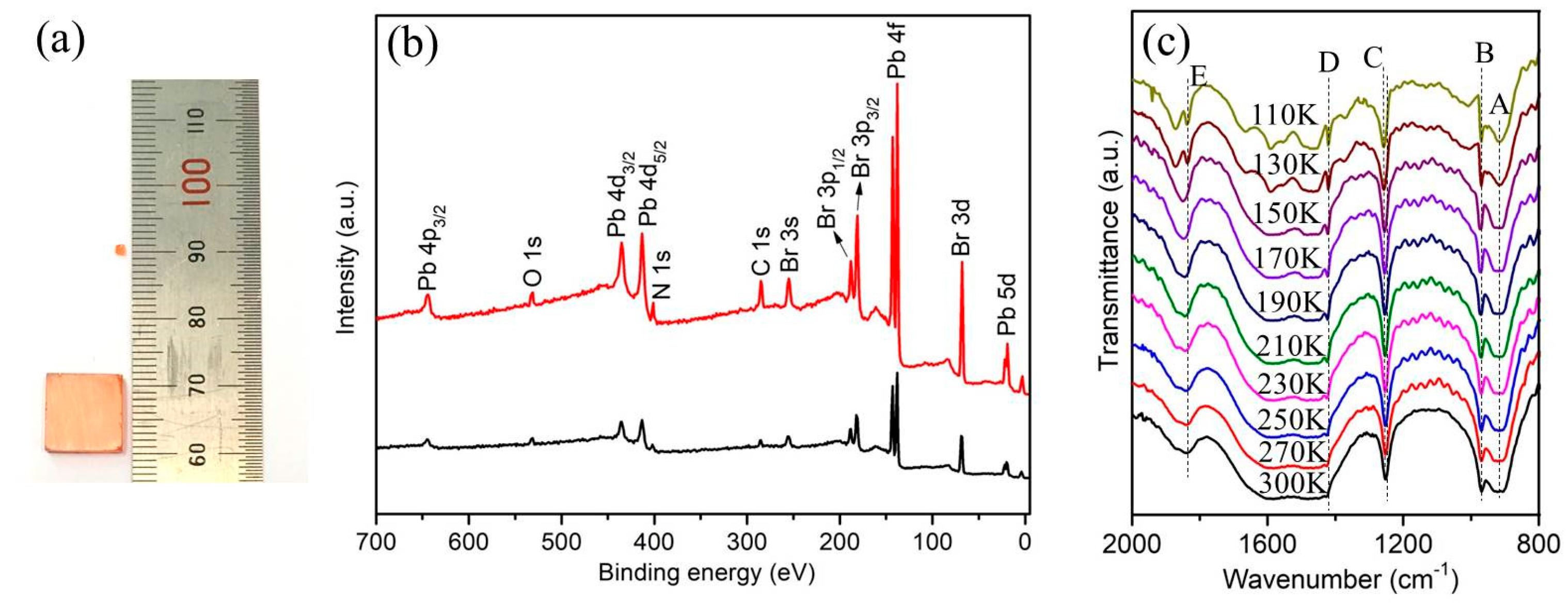
2 in DMF solution through the conventional ITC method. The optical image of the prepared small MAPbBr
3 seeds and large single crystal is shown in
Figure 1a. The sizes of the prepared perovskite crystal seeds are 1-2mm, while the single crystals demonstrate sizes up to a millimeter (11mm×11mm×2 mm). The surfaces of both small seeds and large crystals are quite smooth without cracks, which confirm the uniformity of the preparation. The elemental composition was confirmed by XPS measurements (
Figure 1b), and the analysis suggested a joint contribution of Pb, Br, N and C in the prepared perovskite MAPbBr
3 crystals, whereas the surface O was present in low amounts. Herein, the XPS spectrum analysis indicates that the Pb and Br elements have a mole ratio of ~1:3 for both MAPbBr
3 seeds and large single crystal (see Area N in
Supporting information Table S1), which is in accordance with the stoichiometry of perovskite. The surfaces of the as-prepared Single crystal MAPbBr
3 are quite smooth without cracks, which confirms the uniformity of the preparation (
Supporting information Figure S1).
In situ variable-temperature FTIR measurement was first performed on the MAPbBr
3 crystal at the temperature range of 110–300 K, as shown in
Figure 1c. Organic cationic MA
+, present in MAPBr
3, plays an important role in balancing valence and maintaining the PbBr
6 octahedron in single crystals. The rotation, bending or rocking of different chemical bonds between MA
+ cation and atoms of negative halogens results in different energy changes resulting in different FTIR shifts. All these FTIR bands are related to the motion of MA
+ cations.
Among these FTIR peaks in
Figure 1c, the FTIR band pattern observed at 914 cm
-1 and 972cm
-1 as band A and band B is associated with the CH
3NH
3+ rocking and C-N stretching in MAPbBr
3, while the band C located at 1255cm
-1 is associated with the CH
3-NH
3+ rocking, which is accordance with the reported characteristic peaks in single crystal MAPbBr
3.[
26] As the temperature decreases, the thermal motion of the cation weakens and the peak width of this FTIR band C increases and undergoes a redshift, indicating an increase in MA
+ restricted rotation. In the FTIR spectroscopy results, the FTIR band D (1421cm
-1) strengthened obviously when the temperature decrease down to 130 K. This FTIR band is associated with the NH
3+ bending. Besides, the FTIR band E (1838 cm
-1) is spitted with decreasing temperature, which is owing to the lattice and intramolecular vibrations within the crystal.[
27]
The electrostatic interaction between MA
+ and PbX
6- is controlled by the hydrogen-bonding interactions between the NH
3+ group in MA
+ and the negatively charged halide atoms. Defective states will great affect the lattice and intramolecular vibrations within the crystal. In the study of defects in single crystal MAPbX
3, the formation of vacancy defects (V
MA, V
Br, V
Pb) and cationic antisite defects (MA
Pb, Pb
MA) has little effect on the spatial position of adjacent atoms.[
28] For interstitial methylamine- and methylamine-substituted bromine defects (MA
i, MA
Br), the positional relaxation of the constituting atoms is not obvious, but the cationic property of methylamine has a weak electrostatic effect of attraction or repulsion to the surrounding ions.[
29] At the same time, due to the large volume of Pb atoms and each Pb atom carrying two positive charges, the interstitial defects of lead atoms (Pb
i) and the defect formed by Pb replacing negative bromine (Pb
Br) have a great impact on the surrounding atoms. During crystal growth, if charged defects such as Pb
Br are formed, they may affect the coordination state of the surrounding atoms, break the mode of coordination between Pb and the 6 nearest neighbor Br atoms to form octahedra, form complex ion bond coordination atomic groups, destroy lattice symmetry, hinder further crystal growth, and even form defects such as pores and grain boundaries.[
30] Appropriate material synthesis conditions are needed to inhibit the formation of these defects.
To passivate the defective states induced by interstitial defects of lead atoms (Pb
i) and the charged defects Pb
Br during the large perovskite crystal from small MAPbBr
3 seeds, introducing electronegative small molecules into the precursor solution is probably an effective way to passivate such defects, which favors charge transfer and extraction in X-ray detectors.[
12] In general, under coordinated Pb atoms can act as electronic trap states within the perovskite material in some cases. This under coordination of the Pb atom could result in the formation of a net positive charge on the atom, which would then create favorable conditions for coordination or bond formation with electron-rich molecules. In the case of materials that have a lone pair available for coordination, the electrostatic attraction between the positive charge on the metal and the lone pair could facilitate the formation of a coordinate or dative covalent bond. This positive charge can then be delocalized, and the Pb atom-induced defect states are passivated.
Herein, rich ether-oxygen PEA groups, is employed as an additive to passivate the perovskite surface and grain boundary defects during MAPbBr
3 crystal growth. The PEA additive with different concentration is added to the MAPbBr
3 precursor solution for large crystal growth. The mixed solution was stirred for 2h and filtered before the MAPbBr
3 seed crystals were involved. Pb
2+ ions in perovskite have 6p empty electron orbits. The lone electron pairs from ether-oxygen in PEA can be delocalized to the empty orbits of Pb
2+, forming coordination bonds. The ether-oxygen unshared electron pair activates to form a crosslinking complex with lead ions at the perovskite surfaces and grain boundaries. The optical image of as-prepared MAPbBr
3 single crystal and MAPbBr
3 crystal fabrication with PEA additives were shown in
Figure S2 in supporting information.
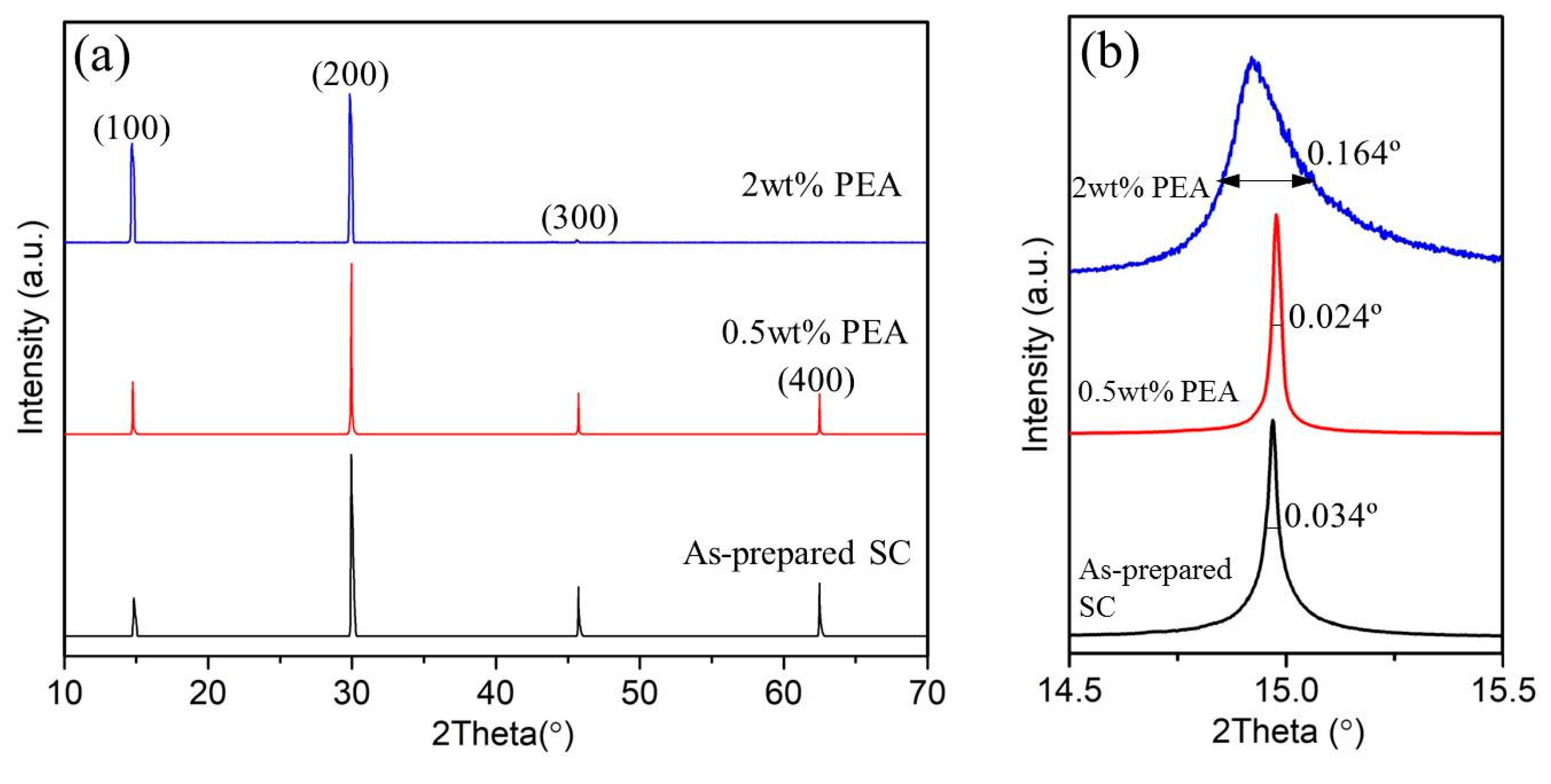
XRD is employed to study the crystal structure of as-prepared MAPbBr
3 single crystals prepared by ITC method, and the crystals fabricated with 0.5wt% PEA and 2wt% PEA additives involved in the precursor solutions, as shown in
Figure 2a. The discontinuous diffraction pattern confirms their single crystal structure with good anisotropic planes. The characteristic diffraction peaks correspond to the (100), (200), (300) and (400) planes confirmed that all samples had a cubic crystal structure and space group no. 221 (PmPm) with lattice constant a = 5.907 Å, which is in consistent to the literature. It is confirmed that the single crystal structure is not changed by PEA additives involving during the crystals growth.
The XRD rocking curve of (100) reflection in MAPbBr
3 single crystals is demonstrated in
Figure 2b. The first major XRD peaks were examined using full width at half maximum (FWHM) to compare the fine crystalline quality of the MAPbBr
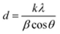
3 crystals. The crystallite sizes can be obtained quantitatively by using the Scherrer equation (equation 1):
where
d is the crystallite size in nanometers;
k is the shape factor constant, which is 0.89;
β is the full width at half maximum in radians;
λ is the wavelength of the X-rays, which is 0.124 nm for the incident synchrotron X-rays; and
θ is the Bragg diffraction angle.[
31]
The FWHM of the as-prepared MAPbBr3 single crystals, crystals with 0.5wt% PEA and 2wt% PEA additives are 0.034°, 0.024° and 0.164°. The crystallite sizes are thus calculated to be 193nm, 273nm, and 40nm, respectively. This result suggests that the optimized quality of 0.5wt% added MAPbBr3 single crystals have the largest crystal size with less grain boundaries and best crystallinity.
In the cubic crystal structure of MAPbBr
3, the methyl ammonium CH
3NH
3+ cations are localized to the area between the two [PbBr
6]
4− octahedral layers. The organic and inorganic components interact by hydrogen bonds between the amino group and the halide ions, whereas weak van der Waals interactions exist among the organic components.[
26] Depending on the occupation and orientation of the organic amino cations, the spacing between the inorganic layers is accordingly changeable. Due to the large volume of Pb atoms and each Pb atom carrying two positive charges, the interstitial defects of lead atoms (Pb
i) and the defect formed by Pb replacing negative bromine (Pb
Br) have a great impact on the surrounding atoms. The introduction of suitable negative charged PEA additives (~0.5wt%) in the precursor DMF solvent, the positive charged metals are probably restricted within the single crystals, reducing the molecular groups twisting and lattice distortion. It is noticed that large amount PEA additives (such as 2wt% PEA) may introduce too much negative species, disrupting the electrical equilibrium during the MAPbBr
3 single crystals growth. As a result, much grain boundary with small crystals are probably generated, as demonstrated in
Figure 2b.
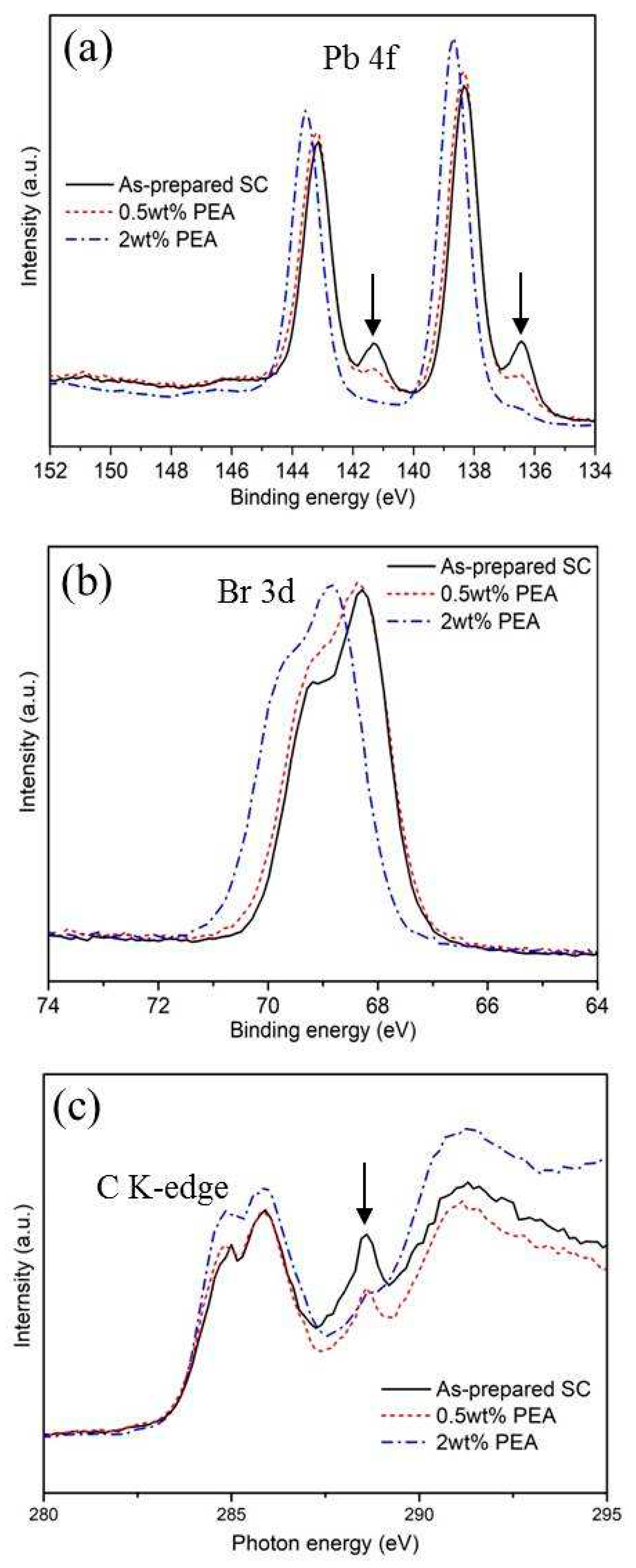
XPS study was performed to examine defect formation during large crystalline MAPbBr
3 growth from seed crystals. The Pb 4f spectra of as-prepared MAPbBr
3 single crystals, and crystals with 0.5wt% PEA and 2wt% PEA additives are shown in Fig. 3a. Two small peaks (see arrows in
Figure 3a) at 136.49 eV and 141.34 eV in the Pb 4f spectrum are observed for the as-prepared single crystal MAPbBr
3 crystal, which is associated with the existence of metallic Pb. The metallic Pb defects are probably associated with the interstitial defects of lead atoms (Pb
i). These defects act as nonradiative recombination centers, hindering carrier transfer and collection and lowering the performance and stability of optoelectronics, including X-ray detectors. With increasing of the PEA additives in solvent during the MAPbBr
3 single crystals growth, the metallic Pb peak is reduced, owing to the passivation of interstitial defects of lead atoms (Pb
i) and reduce the charged defects Pb
Br formed by Pb replacing negative bromine. Meanwhile, the binding energy of Pb 4f
7/2 (4f
5/2) shifts from 138.36 (143.19) eV to 138.68 (143.55) eV to with increasing of PEA additives in solvent. This also shift confirms the increase in the cationic charge of Pb ions in MAPbBr
3.[
32]
Figure 3b depicts the binding energies of Br 3d
3/2/3d
5/2, and the peak positions are centered at 68.6/68.3 eV and 69.3/69.1 for the as-prepared MAPbBr
3 single crystals and 2wt% PEA added MAPbBr
3 crystals, respectively. Consistently, there are approximately 0.2-0.3 eV positive shifts after PEA added crystals. Because the charged defects Pb
Br formed by Pb replace negative bromine during the large crystal growth in the no PEA added MAPbBr
3, the Br 3d in such single crystals have less electron density and lower binding energy, leading to the low peak value of Br 3d. The PEA additives passivate charged Pb
Br defects and increase the binding energy, which is consistent with the observations in the Pb 4f spectra.
To further study the interaction between PEA additives and MAPbBr
3 during the single crystal growth, XANES based on synchrotron radiation was used to detect the electronic structure of large MAPbBr
3 perovskite crystals using the TEY mode. In
Figure 3c, prominent 1s-π
∗ transition between 285 eV and 287 eV can be observed in all three samples. The peak located at 285.0 eV corresponds to C-C (or C-H), while the peak at 285.7 eV is attributed to C-N in MAPbBr
3 crystals.[
33] The obvious peak at 288.6 eV for as-prepared MAPbBr
3 large crystals of the without PEA treatment was attributed to a series of defective states during MAPbBr
3 large crystal growth, resulting in the partial oxidation of the sample surface and producing alkyl functional groups. The peak at 288.6 eV is reduced for the PEA-treated MAPbBr
3 crystals, which confirms the effective passivation of defective states in single crystal MAPbBr
3.
The performance of perovskite single crystals in optoelectronics is severely limited by the presence of large amounts of defects on the surface and crystal boundaries, which greatly restricts energy transfer. To study the relation between X-ray photoelectric conversion and MAPbBr3 single crystals, 40 keV monochromatic X-ray beam with a spot size of 500 μm×500 μm was used to illuminate the single crystal MAPbBr3 perovskites. The bias voltage was applied on the device, and the induced photocurrent was recorded by a Keithley 6517B. Two 50 nm Ag electrodes with 2×2 mm2 were used to deposit on the surface of MAPbBr3 single crystals for I-t and I-V measurements.
The conventional space charge limited current (SCLC) method is employed to investigate the transport properties of a device. The trap density (n
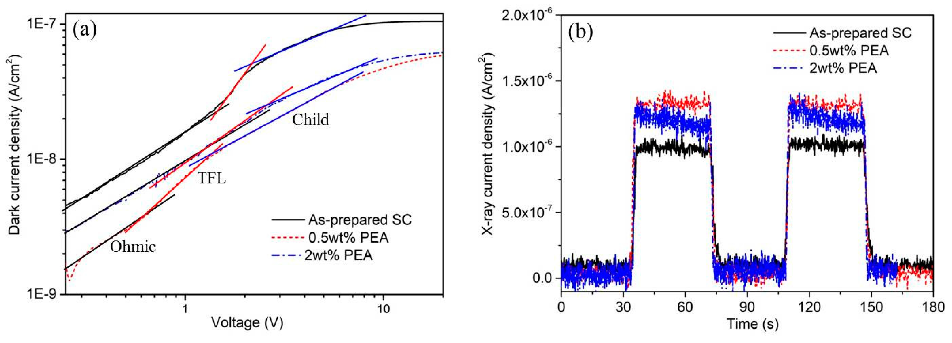
trap) and carrier mobility (μ) of the device can be derived from measuring the dark I–V curve, as shown in
Figure 4a. It shows the dark I–V properties of as-prepared MAPbBr
3 single crystals, and crystals with 0.5wt% PEA and 2wt% PEA additives. The I–V curves are divided into three regions: ohmic (black line), trap filling region (red line), and trap free (blue line). The trap density (n
trap) can then be determined by the trap-filled limit voltage, VTFL, the voltage at which the current begins to increase rapidly using the following equation (equation 2):
where ε
0 is the vacuum permittivity, ε
r is the relative dielectric constant (ε
r = 25.5), e is the elementary charge (1.6×10
−19 C), and L is the single-crystal thickness (~2mm).[
34] The trap densities of single crystals with different dissolved temperatures were determined according to the equation (see
Table 1).
By comparing the carrier transport of MAPbBr3 single crystals fabricated in different solvent components, the MAPbBr3 crystals generated using 0.5 wt% PEA additives have the lowest trap densities, which further confirms that the suitable PEA treatment will effective passivate the defective states during the MAPbBr3 single crystal growth.
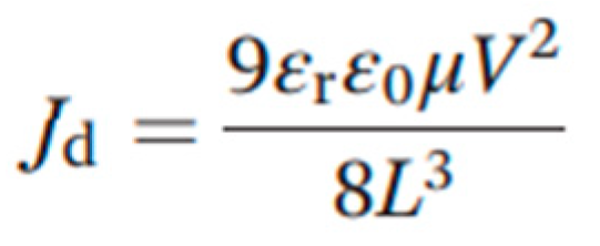
The carrier mobility over approximately 10 V of the single crystal was extracted by fitting the Mott–Gurney law (equation 3):
where J
d is the dark current density, µ is the mobility, and V is the voltage.[
34] The mobility of the MAPbBr
3 single crystal with 0.5 wt% PEA additive was 1.57 cm
2 V
−1s
−1, while it is 3.15 cm
2 V
−1s
−1. Meanwhile, the conductivity of MAPbBr
3 single crystals in dark condition can be calculated in the Ohmic region in
Figure 4a. It is found that both conductivity and mobility of PEA treated MAPbBr
3 are relatively lower than that of the as-prepared MAPbBr
3 single crystals in dark condition. This can be explained that the PEA passivation decrease the defect states, so that the hole concentration from are defective donors are inhibited in such “perfect” MAPbBr
3 single crystal.
Figure 5b shows the time-dependent photo response of the single crystal device under 40 keV X-ray generated by the synchrotron source with 200mA beam current. The photon flux at the sample position is ~2×10
10 phs/s/mm
2. Herein, the spot size of 500μm×500μm was used to illuminate the single crystal MAPbBr
3 perovskites, the dose level is calculated to be ~0.135 Sv. A photocurrent of 1.35×10
−6 A cm
−2 and 1.25×10
−6 A cm
−2 at a bias of 10 V for the 0.5 wt% and 2wt% PEA-treated MAPbBr
3 crystal can be seen in Figure 4b, obviously higher than the 9.8 × 10
−7 A cm
−2 for the as-prepared MAPbBr
3 single crystal without PEA treatment. The calculated photocurrent is improved 27.4% for the 0.5 wt% PEA treated crystal samples and improved 20% for the 0.5wt% and 2wt% PEA-treated crystal samples respectively. Similarly, the improvement of photocurrent of the PEA-treated MAPbBr
3 single crystals can also be observed with low dose X-ray exposures (5mA synchrotron beam current, ~3.4 mSv), as shown in
Figure S3(Supporting information) .
After we evaluated the X-ray performance by directly comparing the as-prepared MAPbBr3 single crystals and the PEA-treated crystal samples, we can see that the 0.5 wt% PEA-treated crystal samples show the best X-ray response and charge collection efficiency, reflecting the excellent photogenerated carrier transport properties of the PEA-treated MAPbBr3 single crystal. This excellent carrier transport probably results from a reduced defect density by PEA passivation, leading to a low trap density and dislocation density during MAPbBr3 single crystal growth.
Figure 4.
(a) Dark I–V characteristics of MAPbBr3 single crystals without and with 0.5wt% and 2wt% PEA additives exhibiting different regions obtained from the log I versus log V plot. (b) Temporal response of the detectors photocurrent density under high dose X-ray illumination.
Figure 4.
(a) Dark I–V characteristics of MAPbBr3 single crystals without and with 0.5wt% and 2wt% PEA additives exhibiting different regions obtained from the log I versus log V plot. (b) Temporal response of the detectors photocurrent density under high dose X-ray illumination.
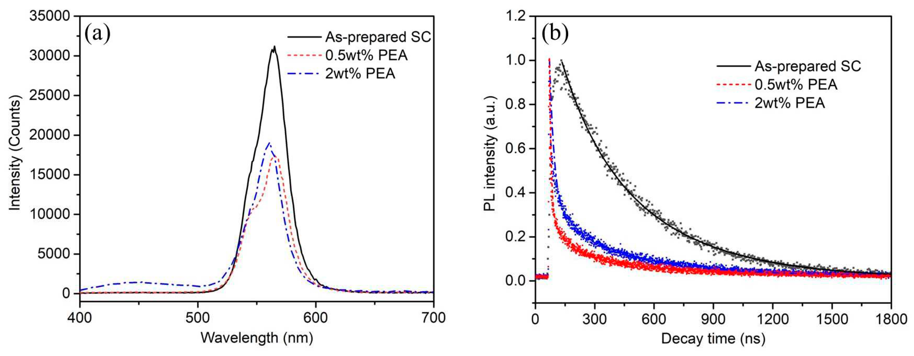
Photoluminescence and TRPL spectroscopy were employed to study the surface/interfacial charge and defects of PEA added MAPbBr
3 crystals, as shown in
Figure 5. The MAPbBr
3 NCs show an emission peak at ≈560 nm, corresponding to its direct band gap of 2.2eV. Compared to MAPbBr
3 crystals, the PL emission of MAPbBr
3 NCs at 560 nm was intensively quenched when they were decorated on PEA additives during their crystal growth (Figure 6a). The PL intensity dropped about 40% for the sample MAPbBr
3 with 0.5% PEA additives. The dramatically reduced PL intensity of MAPbBr
3 after hybridization with PEA suggests effective charge and/or energy transfer with less surface defects.
The charge and/or energy transfer of MAPbBr
3 crystals were further investigated by the TRPL spectroscopy measurements. We characterized the carrier recombination processes by monitoring the TRPL decay traces of MAPbBr
3 NCs at ~560 nm as shown in Figure 5b. The PL lifetime of as prepared MAPbBr
3 single crystals, 0.5%wt and 2wt% PEA treated MAPbBr
3 crystals can be well fitted with triple-exponential decay kinetics as shown in
Table 1, which suggests different emitting species exist in MAPbBr
3 crystals with different additives. It is observed that the PL lifetime of MAPbBr
3 NCs was intensively shortened when PEA additives were involved in their crystals growth.
This is probably caused by the lowering of defective trap states (Pb
Br defects et al.) in MAPbBr
3 NCs, which is in accordance with the XPS analysis (
Figure 3) and photocurrent response study (
Figure 4b). Some of the MAPbBr
3 NCs with PEA additives are expected to passivate the perovskite surface and GB defects during crystal growth. Pb
2+ ions in perovskite have 6p empty electron orbits. The lone electron pairs from ether-oxygen in PEA delocalized to the empty orbits of Pb
2+, forming coordination bonds. The ether-oxygen unshared electron pair activates to form a crosslinking complex with lead ions at the perovskite surface and GBs. The charge and/or energy transfer rate and efficiency are largely depended on the interactions between MAPbBr
3 and PEA additives, thus leading to different emitting species. Similar multiexponential decay kinetics is observed in the solution growth perovskite crystals, while the effective decay lifetime (τ
eff) can be used to indicate the entire charge and/or energy transfer rate in the MAPbBr
3 NCs grown in different conditions.
Fluorescence decay profile can be fitted by a two exponential function, I(t)=A0+A1×exp(-t/τ
1)+A2×exp(-t/τ
2), where τ
1 and τ
2 denote the decay times for the faster and the slower component, respectively, and A1 and A2 are the amplitudes,[
35] as presented in
Table 2. The dominant faster lifetimes τ
1 are 180 ns, 9.5 ns and 25.7 ns for the MAPbBr
3 NCs fabricated without PEA, and 0.5% PEA and 2% PEA additives. Meanwhile, their slower lifetimes τ
2 are 460 ns, 210 ns and 360 ns respectively. The faster and slower decay represent the dielectric environment related non-radiative recombination and free exciton recombination, respectively. The largely shortened PL decay lifetime by introducing the content of PEA additives, indicating the effective charge and/or energy transfer on the MAPbBr
3 NCs with PEA additives.
Then the charge and/or energy transfer rate (k
T) was estimated based on the following equation (equation 4):
The calculated results indicate that the kT value of MAPbBr3 was ≈0.0006 s-1 for 2wt% PEA additives, whereas the kT was 0.0025 s-1 for 0.5wt% PEA additives, respectively. The charge and/or energy transfer rate are largely depended on the bonding between MAPbBr3 and PEA molecules, reducing the defects on MAPbBr3 crystals surfaces. It indicates that the 0.5wt% PEA is the best quantity for defect passivation. Overall, the decay time of MAPbBr3 single crystal is decreased from 460 ns to 210 ns in free exciton recombination by TRPL decay measurement, owing to the defect passivation. The PEA-treated single crystals have much faster than the commercialized Ce:YAG scintillator (>500ns). The shorter decay time demonstrate its potential application in fast X-ray pulse detection, especially in the MHz high repetition synchrotron and ultra-fast XFEL pulse diagnosis.
Figure 5.
(a) PL spectra, and (b) TRPL spectra of the MAPbBr3 crystals, and MAPbBr3 crystals with 0.5% PEA and 2% PEA additives in their growth of crystals.
Figure 5.
(a) PL spectra, and (b) TRPL spectra of the MAPbBr3 crystals, and MAPbBr3 crystals with 0.5% PEA and 2% PEA additives in their growth of crystals.
