Preprint
Article

Clock Mesh Synthesis Methodology Based on Combinatorial Optimization

Altmetrics

Downloads

213

Views

98

Comments

0

Submitted:

08 September 2023

Posted:

11 September 2023

You are already at the latest version

Alerts
Abstract
In light of advancing technology, the conventional clock network architecture has become inadequate for addressing the intricacies inherent in modern System-on-Chip (SoC) designs. While clock mesh topology offers resilience against On-Chip Variation (OCV) fluctuations, it still necessitates manual intervention. Therefore, substantial scope exists for methodological enhancements and the refinement of rapid analytical techniques. This paper introduces a novel clock mesh synthesis approach, underpinned by dynamic programming algorithms, that guarantees latency constraints. Our experimental findings demonstrate that our algorithm achieves an additional 26.6% reduction in power consumption compared to the baseline methodology. Furthermore, it substantially reduces runtime by an average of 78.0% when contrasted with traditional simulation methods. These results highlight the potential of our methodology for enhancing the efficiency and power management of clock mesh.
Keywords: 
Subject: Computer Science and Mathematics  -   Hardware and Architecture

1. Introduction

Multiple PVT corners, clock domains, and low power requirements have made the design of clock distribution network (CDN) a challenging problem. Except for affecting the frequency of SoC, CDN can even contribute more than 40% among the overall chip power consumption [1,2,3,4,5]. As the technology of semiconductor process is scaling down to 10nm and below, clock mesh has structural advantage against On-Chip Variation (OCV) effects.
To explore the improvement space in this research field, we review the existing works on clock mesh network. In the early 2000s, IBM proposed its clock distribution strategy implemented on several microprocessor chips [1,6,7,8,9,10]. The works of [11,12,13] also applied custom or semi-custom mesh design like the work of [1], and did not address the problem of automatic mesh synthesis or optimization. To address these drawbacks above, David Z. Pan et al. [14,15,16] proposed their clock mesh synthesis framework. In this work, they first discussed the mesh window planning problem and concluded how the wire length changes with different mesh sizes without physical information based on linear programming. To save power consumption, this paper et al. also discussed the possibility of deleting some mesh edges which has little effect on final performance. So there is a trend to build non-uniform clock mesh in recent research works, not only for power saving but handling the distribution of unbalanced loads. This paper [17] proposed a non-uniform clock mesh by using an efficient graph-theoretic and geometric quasi-linear algorithm, and this algorithm can reduce mesh wires more aggressively. Unluckily, constraint graph extraction is computationally expensive, and it is not easy to prove the reliability in physical design. This research also lacks considering load balancing and wire width variation. Another research work on non-uniform clock mesh is presented in the paper of [16], they have proposed two phases to finish the clock mesh synthesis based on a binary linear programming algorithm. The first phase explores various (both regular and irregular) clock mesh configurations. Once a clock mesh configuration is determined, the second phase includes the binary linear programming which is applied to assign each sink to the least-load mesh segment to improve slew and skew. Although they have solved the trade-off between capacitance and skew and targeted for more uniform load capacitance distribution, the wire width variation of clock mesh is still unmentioned and the local clock quality of mesh window is difficult to control. The work of [18] presented the first non-greedy buffer placement and sizing technique using linear programming (LP) and iterative buffer removal. This work [18] considered non-uniform mesh placement by moving edge locations directly. However, the benchmarks they used were very simple to prove their effectiveness in some large designs, and the wire width parameter is also not studied. Baris et al. proposed their work of clock mesh and synthesis with incremental register placement [19,20,21,22]. Feasible moving regions are built based on timing slack constraints, and this work combines incremental register placement with non-uniform clock mesh generation. But the number of registers increasing, the computational complexity may not be controlled easily. Detailed parameters, like the wire width, are also not mentioned. By reviewing the above work, we find that it is necessary to optimize the methodological flow of clock mesh to avoid an excessive design iteration process. Design goals can be based on latency metrics, and appropriate design slack can lead to wire length optimization. Additionally, local design rules are easier to analyze and control the output quality.
The major contributions of this paper are highlighted as follows. We propose a novel methodology that can greatly improve the efficiency of clock mesh synthesis with latency-bounded constraints. Based on a dynamic programming algorithm, we can automate mesh topology design for complex layout scenarios after the placement stage. We modified the mesh window modeling with wire width consideration. Based on the benchmark circuits, we verify the effectiveness of the methodology. In addition, we also performed layout verification.
The rest of this paper is organized as follows. Section 2 introduces the preliminaries of this work. Section 3 presents details of our methodology and algorithm details. Section 4 demonstrated the experimental results. Finally, Section 5 concludes the paper.

2. Preliminaries

This section will review the background and problem formulation. The primary clock mesh structure is shown in Figure 1. From the clock source, the global clock trees which are also called the pre-mesh trees are used to drive the clock mesh with tap-cells. The tap-cells are the buffer divers to control the drive capability and provide isolation. The local clock clusters, also called the post-mesh trees, are made to drive all sinks (registers).
Key result parameters for CDNs include performance and power consumption. Performance is expressed in clock skew and clock slew, and designers want precise control. The clock skew means the latency difference between clock sinks according to the same clock source. We also consider the slew constraint which represents the transition rate of the clock signal from 0 to 1. The power dissipation can be calculated statistically based on the capacitance value since the design frequency and voltage usually do not change. We can see that many research works only count the wire length of the CDN, and the wire width parameter is not taken into account. At present, the global clock tree structure and local clock tree based on H-tree have appeared, and can accurately control the delay [23,24], but it has not been seen in the design of the mesh itself. On the other hand, the power consumption overhead of mesh needs to be further controlled. To build the mesh formulation, we need to split the CDN’s resulting impact composition.
We formulate the power consumption overhead as the sum of the power consumption of the various parts, which is defined in the formula (1). The power value includes the sum of static and dynamic power consumption. P C D N denotes the power value of CDN. The P G l o b a l , P M e s h , and P L o c a l represent the power consumption values of global clock trees, clock mesh, and local clock clusters, respectively. In the formula (2), S k e w C D N denotes the worst clock skew combination value of the whole CDN. The S k e w G l o b a l , S k e w M e s h , and S k e w L o c a l represent the clock skew values of global clock trees, clock mesh, and local clock clusters, respectively. In recent years, some clock tree synthesis methods for latency constraints have been proposed, which are easier to model than clock skew in some situations. Therefore, we modify formula (2) into formula (3). The L G H L G L means the absolute value of the difference between the highest latency value and the lowest latency value in the global clock trees. The L M H L M L means the absolute value of the difference between the highest latency value and the lowest latency value in the clock mesh. The L L H L L L means the absolute value of the difference between the highest latency value and the lowest latency value in the local clock clusters. In this way, we have converted the clock skew calculation into clock latency calculation.
P C D N = P G l o b a l + P M e s h + P L o c a l
S k e w C D N = S k e w G l o b a l + S k e w M e s h + S k e w L o c a l
S k e w C D N = L G H L G L + L M H L M L + L L H L L L
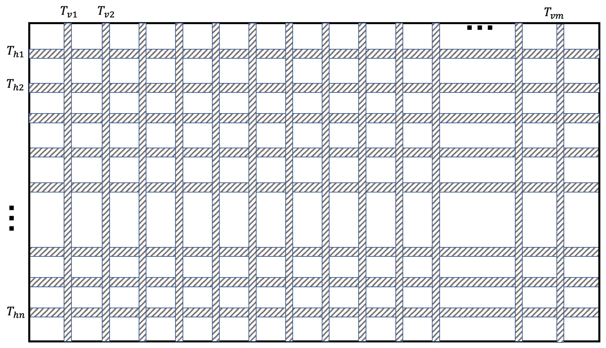
A series of studies in the past is based on the overall mesh planning method, which is only carried out for the main mesh lines, and the scale of the circuit is not large. Traditional planning algorithms are extremely inaccurate when the circuit size increases substantially. Routing tracks are the most fine-grained routing resources in the layout, and using them as the starting state of a mesh network is an ideal problem model. The mesh itself becomes dense, resulting in more redundancy. With the continuous development of algorithms and computing power, we can consider the routing track of clock mesh in more detail, as shown in Figure 2. T v m denotes the routing track in mth vertical space. T h n denotes the routing track in the nth horizontal space. Each mesh window is formed by the intersection of tracks in different directions. In other words, each mesh window affects the state of the associated tracks.
We consider the problem of constructing the clock mesh under the PVT variations. We assume that global clock trees and local clock clusters can be designed and controlled well. Without any circuit information between sinks, we describe this mesh problem as followings.
Inputs: Given a placed design with a set of N clock fixed sinks S = { s 1 , s 2 , . . . , s n } , the clock source location, the layout region, clock constraints and PVT parameters.
Outputs: A clock mesh with appropriate planning, topology generation, and routing resources such that the given design constraints are likely to be satisfied.

3. Approach

3.1. Proposed Methodology

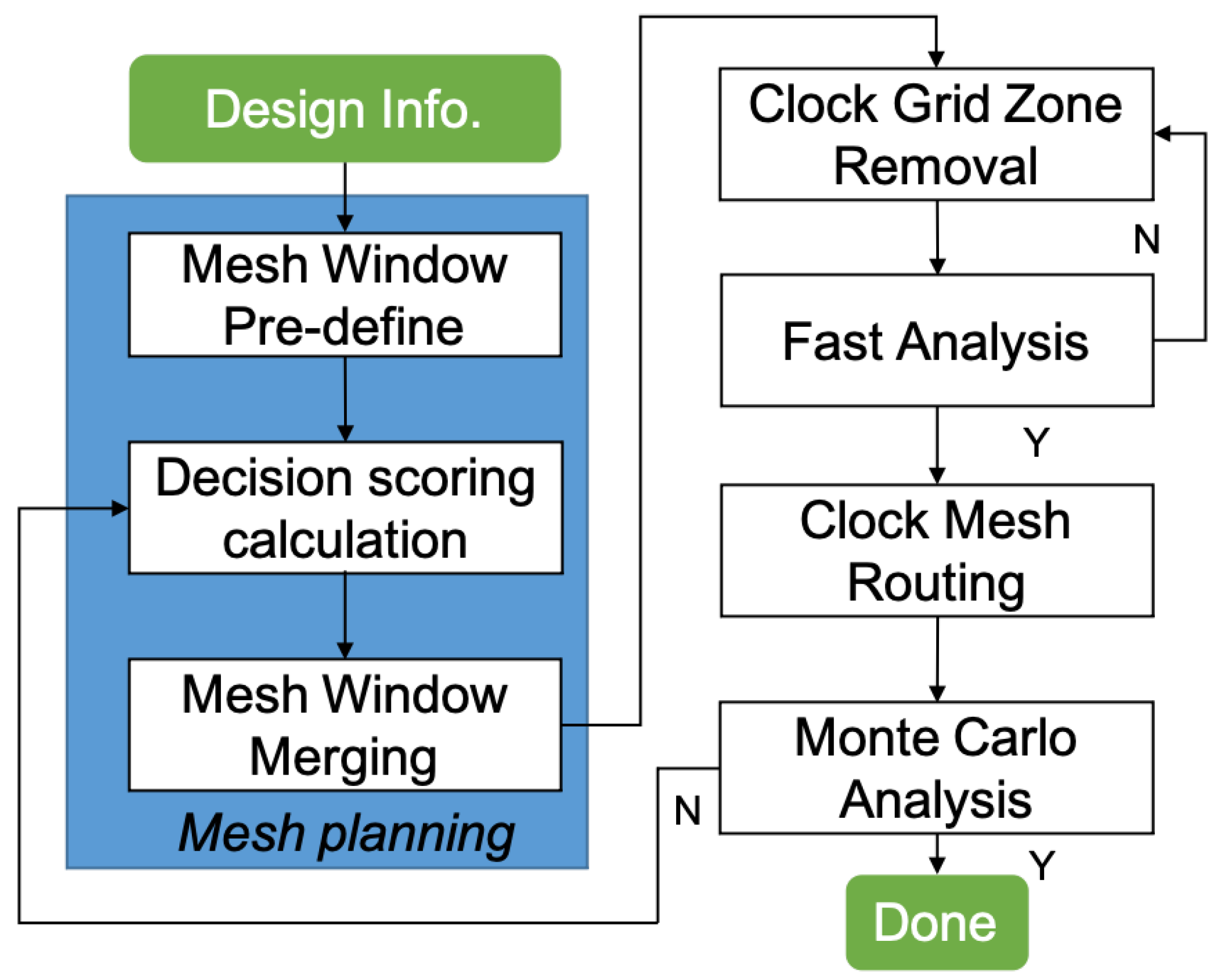
To solve the clock mesh problem, we propose a latency-bounded clock mesh synthesis flow as shown in Figure 3. Given the design information, we firstly focus on the mesh planning process which includes the mesh window pre-define, decision scoring calculation, and mesh window merging. After finishing mesh planning, clock grid zone removal can be applied. Next, fast analysis is integrated to determine whether the mesh topology design is complete. If the design constraints are not met, the design process can be backtracked to the previous stage. After the mesh topology is solidified, basic mesh routing can be carried out. After this stage is completed, we can extract circuit parameters and perform the Monte Carlo SPICE analysis. Based on the analysis results, we can iteratively correct the decision scoring calculation process factors. Eventually, we can reach an offline clock mesh synthesis model.

3.2. Mesh Planning

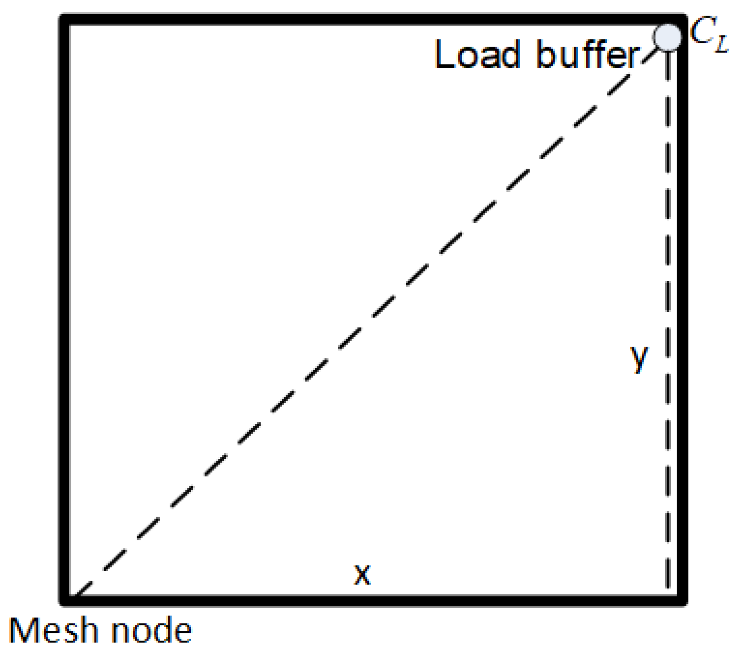
For saving runtime, there exists a need to have a fast analysis for clock mesh analytically. The clock skew value is the biggest concern among all timing constraints. For clock mesh, we assume that the clock skew is the difference in latency values for mesh buffers from the same clock source. The worst case for this value is when one sink is just located on the mesh node which connects with the driving buffer while the other sink locates on the diagonal position, as shown in Figure 4. Thus, the clock mesh window method is considered for solving the skew model for clock mesh [25]. In the paper of [14], they only proposed the skew model by using a simplified RC network which aims to solve the grid sizing problem without consideration of the wire width parameter.
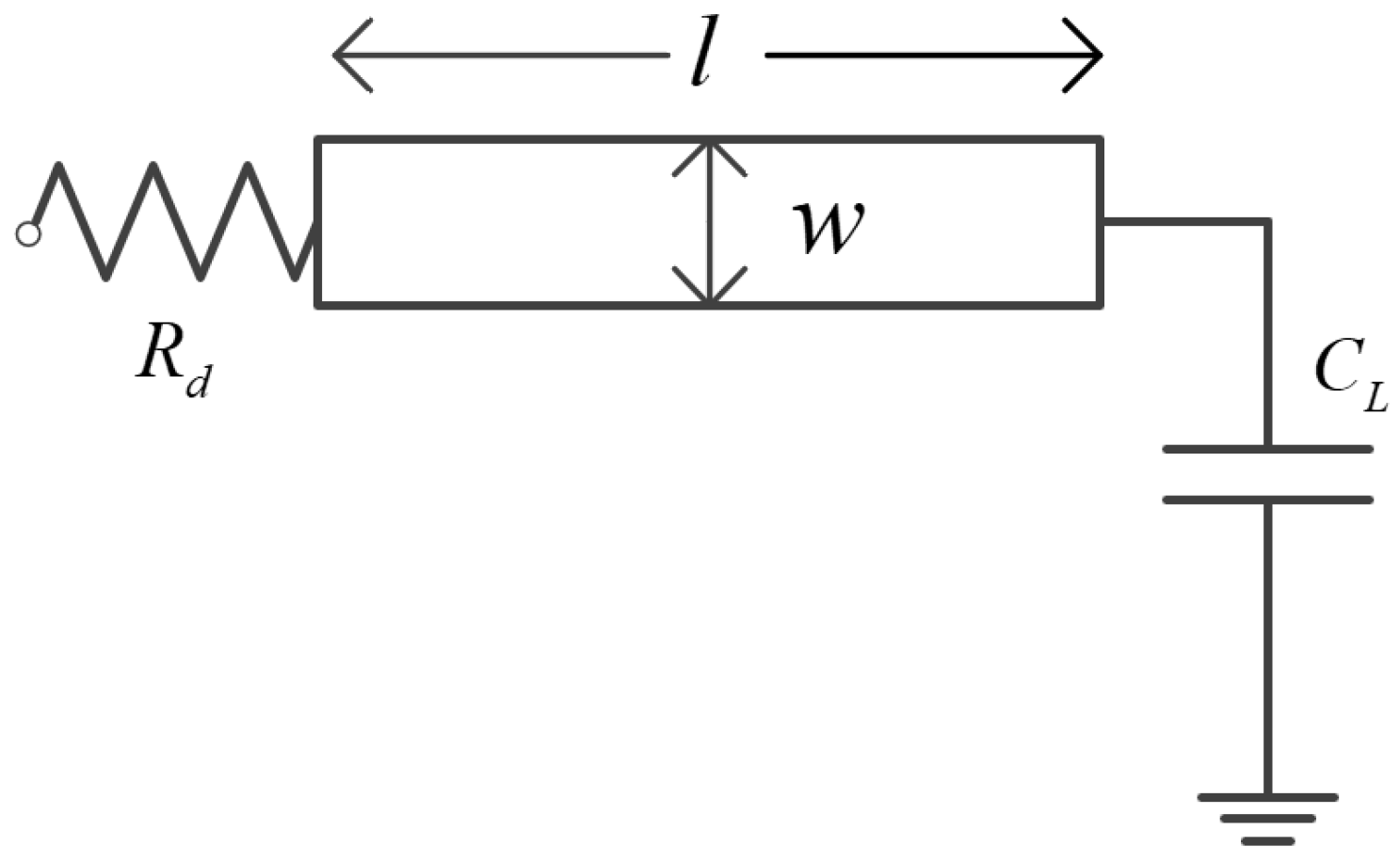
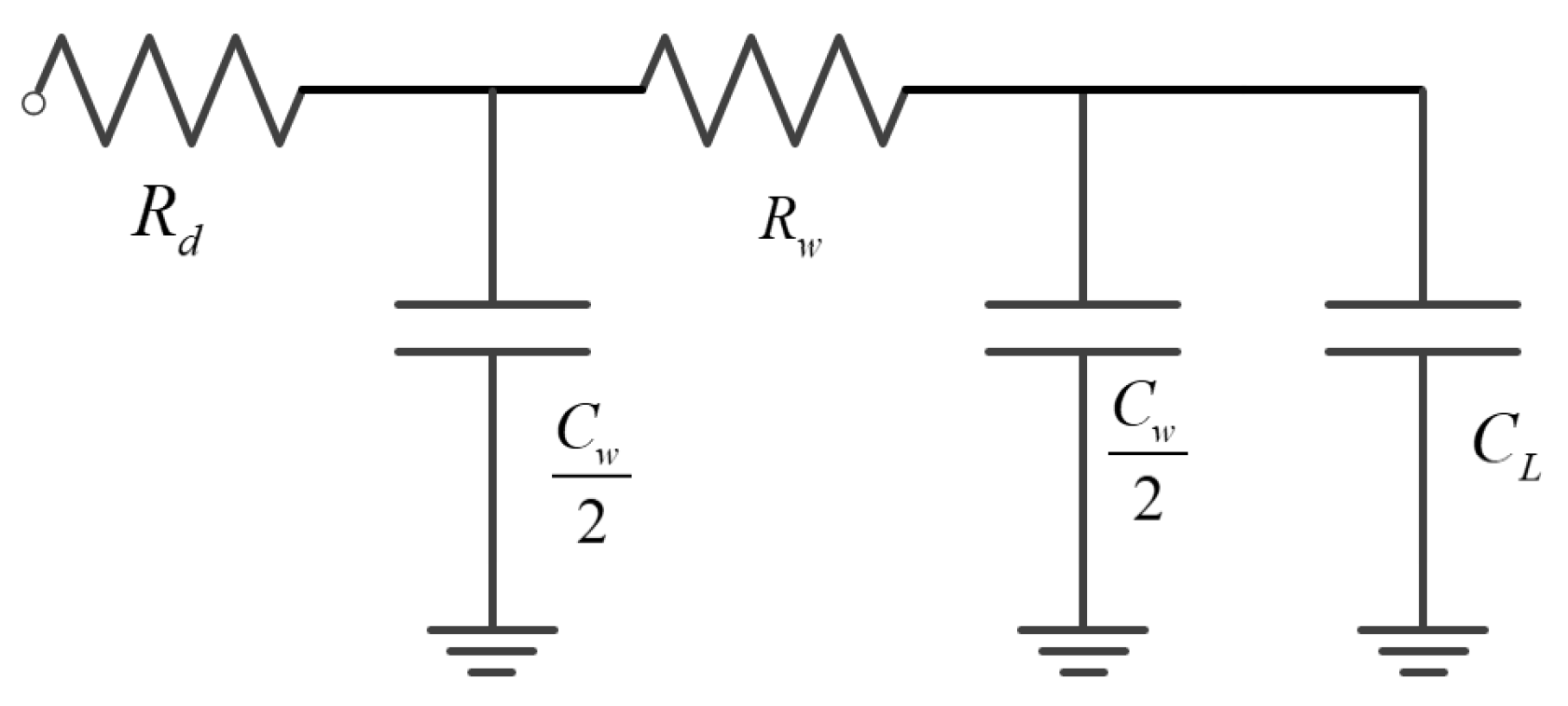
To make the analytical method integrated with the wire parameters possible, we have introduced the interconnect model for the clock mesh window. Given an interconnect of length l with the loading capacitance C L and driver resistance R d , as shown in Figure 5. The interconnect problem is to determine the best uniform width that minimizes the source-to-sink delay. The r represents the sheet resistance, c a represents the unit area capacitance, and c f represents the unit effective-fringing capacitance. To compute the distributed Elmore delay, the original wire is often divided into many small wire segments and each wire segment is modeled as a π -type model, it can be shown that the Elmore delay is the same no matter how the wire is divided into shorter wire segments. Therefore, we can just use the one-segment π -type model as in Figure 6, where R w denotes the total wire resistance and C w denotes the total wire capacitance. The Elmore delay from the driver to the load in Figure 4 can then be written as follows:
T w , l = R d c f l + R d C L + 1 2 r c a · l 2 + R d c a l · w + 1 2 r c f l 2 + r l C L · 1 w
For the example of Figure 4, the distance l is the sum of x and y, and the latency value can be computed. With the fixed buffer type, we only care about the value of l which reflects the Manhattan distance from the mesh node to potential sinks. Parameters for wire can be selected from basic technology files. Additionally, another constraint for the evaluation of wire area A is listed as follows.
A = w * l l
Based on formula (3), the estimated delay can be converted into the skew value calculation. Thus, hard constraints include latency and skew value. We also have introduced some soft constraints and parameters for consideration that can reflect the mesh topology quality. Given an index set I = {1, 2, ..., i} of potential mesh topology, the penalty score formula is defined as follows. For each clock mesh, the W L i represents the whole wire length which includes the mesh and stub (the sum value of the Manhattan distance from mesh wire to all sinks) wire resource, the A i represents the wire area value including mesh and stub resource. In formula (7), we introduce σ i parameter which is the variance of clock delay to reflect the resistance to OCV effects. The L s t represents the latency value from each mesh window, which is noted in Figure 7. The L s t ¯ is the mean value from collected L s t data. With consideration of PVT conditions, we set the margin 15% up and down for L s t calculation. The variable factor weights are represented by α , β , and γ , respectively. We set these weight values to indicate the importance of a certain factor to balance different terms in the score function.
s c o r e i = α · W L i + β · A i + γ · σ i , i I
δ i = L s t L s t ¯ 2 s * t
s * t , s , t { T v m , T h n }
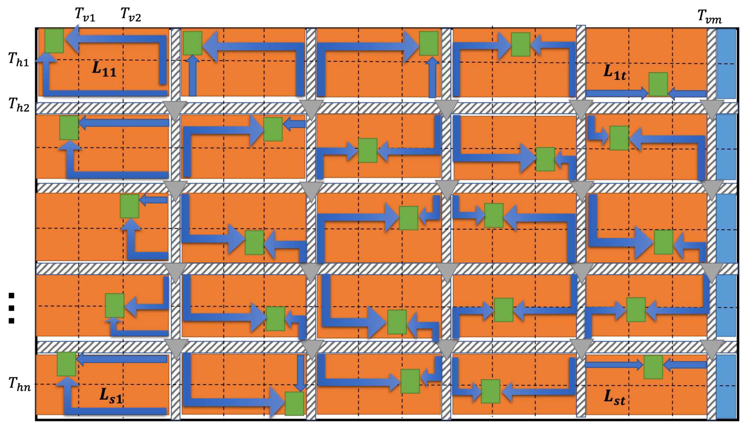
Next, we need to solve the topological set I of the clock mesh. To compress the solution space, we provide a numerical range interface based on engineering experience guidance s * t , such as 5*5 to 30*30, and the general expression for its application is shown in the formula (8). In Figure 7 (this figure strictly follows the model of Figure 2), the mesh planning state is described with a potential merging pattern. With the M p a t t e r n 2 , 3 , the dotted line is removed from the original clock mesh model in Figure 2. In order to reduce computational complexity, each window selects the most critical sink based on the skew value of the maximum and minimum distance from mesh buffers, and the figure identifies the longest and shortest Manhattan distances for each sink by blue arrows. Since there are redundant areas in the layout segmentation, such as the blue rectangles in Figure 7, the window is calculated or not calculated based on the sink distribution. For mesh planning phase, the input physical information includes layout size information { W , H } , track information { T v m , T h n } , sinks set S, physical library and engineering experience guidance s * t . The mesh window merging pattern set M p a t t e r n can be computed based on { W , H } , { T v m , T h n } and s * t . The latency-bounded value L b can also be defined by designers. In this work, only regularized clock mesh generation is considered. We compute and store the s c o r e i and M p a t t e r n for each mesh planning state, and return the optimal strategy with the minimal s c o r e i value.
In Algorithm 1, the mesh planning phase is done based on dynamic programming with different mesh planning states. The first step is the mesh window pre-define which is mentioned in Figure 3.
Given the input information, we collect the merging pattern set M p a t t e r n for the clock mesh in line 2 ( s and t represent stepping strategy values in different directions, respectively), and topological set I can also be obtained. Additionally, we round up to preserve integer data in a pair data structure like in the Figure 7 example. The second step is decision scoring calculation. Based on all potential mesh planning states, we calculate the score penalty score value s c o r e i based on M p a t t e r n , mesh wire width optional information R w i d t h , and the set S of key sinks. During this procedure, the multi-thread technology can be applied due to no data coupling. Data that does not meet key constraints are not retained to optimize data structure space which is described between lines 6 and 9. Then we can easily find the minimal value in the vector s t o r e and return the corresponding mesh planning strategy M E S H t o p , which means the mesh window merging strategy in Figure 3. The above algorithm is efficiently implemented with the help of the analytical latency model, and optimized mesh planning can be obtained.
Algorithm 1 The mesh planning phase
Input: 
The layout size information { W , H } , track information { T v m , T h n } , the set S of key sinks, engineering experience guidance s * t , latency-bounded value L b , and physical library.
Output: 
The clock mesh topology M E S H t o p .
1:
for s 0 , t 0 , s , t do
2:
    I M p a t t e r n ( T h m s 0 + s , T v m t 0 + t ) ;
3:
end for
4:
for all M p a t t e r n , R w i d t h , Sdo
5:
    Calculate each s c o r e i value with multi-threads;
6:
    if MAX( L s , t ) < L b  then
7:
        Push back s c o r e i into vector s c o r e ;
8:
    elseContinue;
9:
    end if
10:
end for
11:
for vector s c o r e with topological set I in hash table do
12:
    Find the minimal value and return M E S H t o p
13:
end for

3.3. Mesh Synthesis

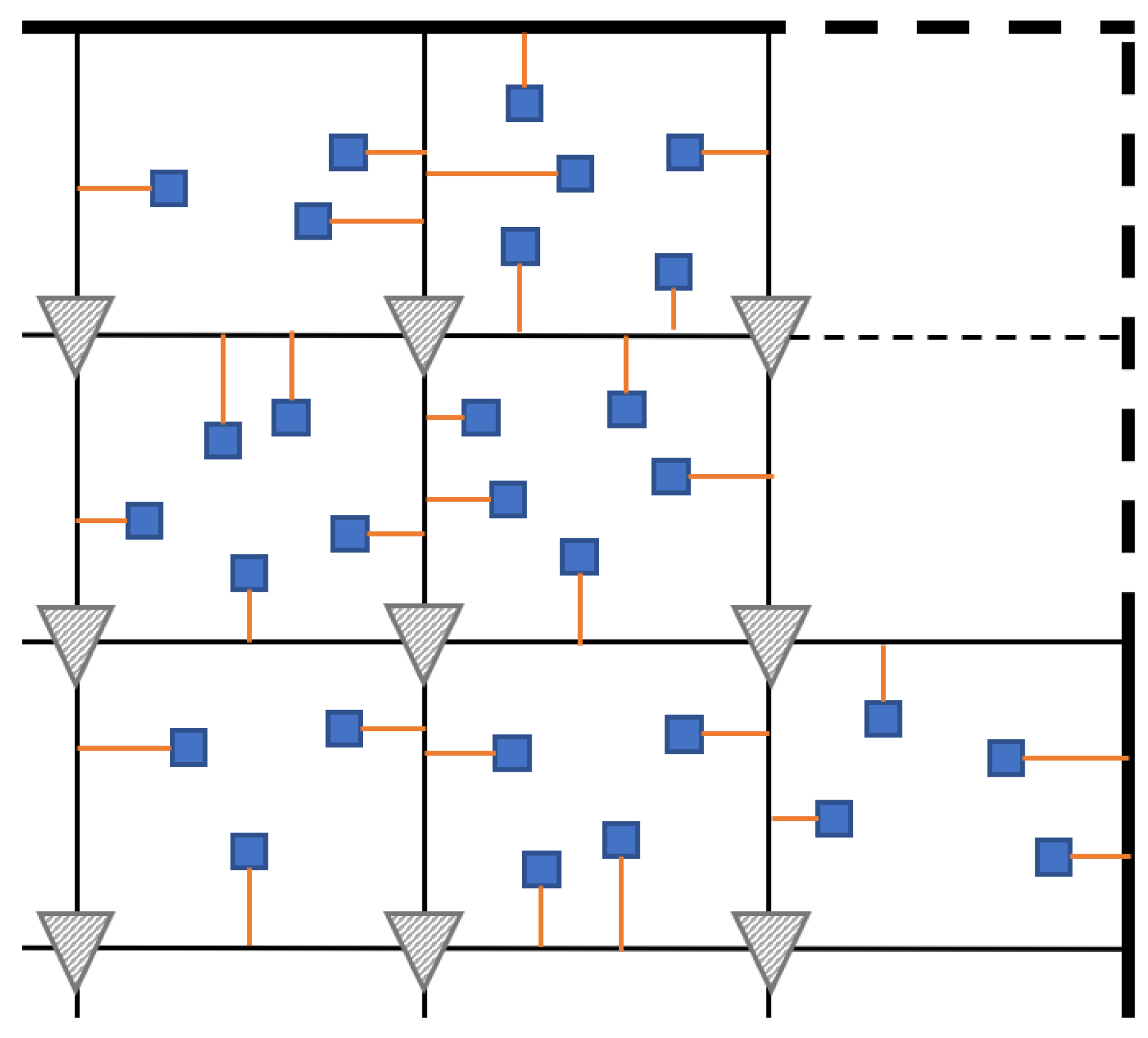
In our proposed methodology, we have integrated the clock grid zone removal procedure and simulation methodology. An example is shown in Figure 8, and dotted lines identify the wire to be deleted. To minimize the mesh wire length without significantly affecting the variation tolerance, the mesh segments that are not critical should be removed. After that, a quick Monte Carlo analysis (maximum clock skew and slew can be checked) can be performed on the related windows to determine whether the necessary constraints are met. In the clock mesh routing stage, detailed routing is done according to the clock mesh topology. After the sink point, direct connection topology, and clock routing are completed, an accurate Monte Carlo simulation can be performed to evaluate the experimental results, correct the weights and strategies to ensure the consistency of the results under specific process conditions, and finally form a methodology that can be applied offline.

4. Experimental Results

The proposed algorithms are implemented in Python with the PyMP library and experiments are performed on a quad-core 3.50 GHz Linux machine with 128 GB of memory. In Table 1, we use the technical data from ISPD2010 benchmarks (BM.) [26], and we have updated the wire parameters to fit this problem formulation without buffer problem consideration, which is similar to advanced process nodes. The baseline experiment [27] is performed on our workstation which is Run.0. We set the latency value (LAT.) to be the constrain, and the mesh grid (M*N) results are based on the score computed. The results of penalty score (SC.) and area reduction percentage are listed as follows, which reflect the wire resource saving. The running results of our runtime (Run.1) are listed in Table 1. Compared with the baseline, the evaluation speedup ratio has reached 2.17X on average.
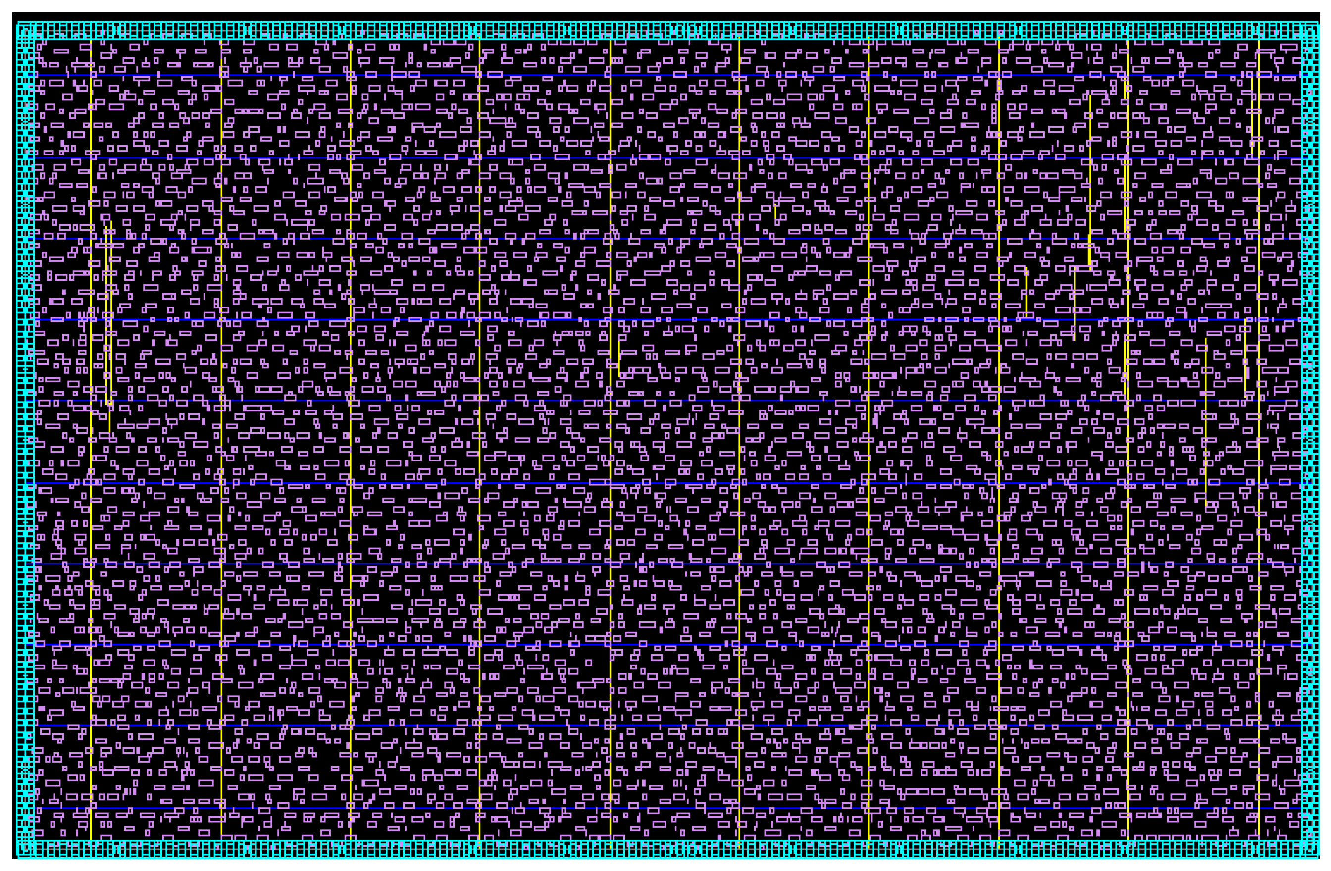
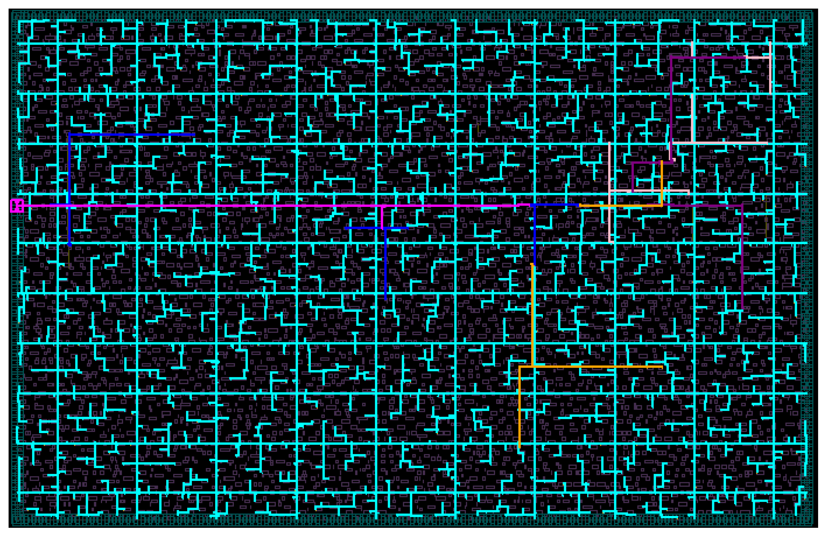
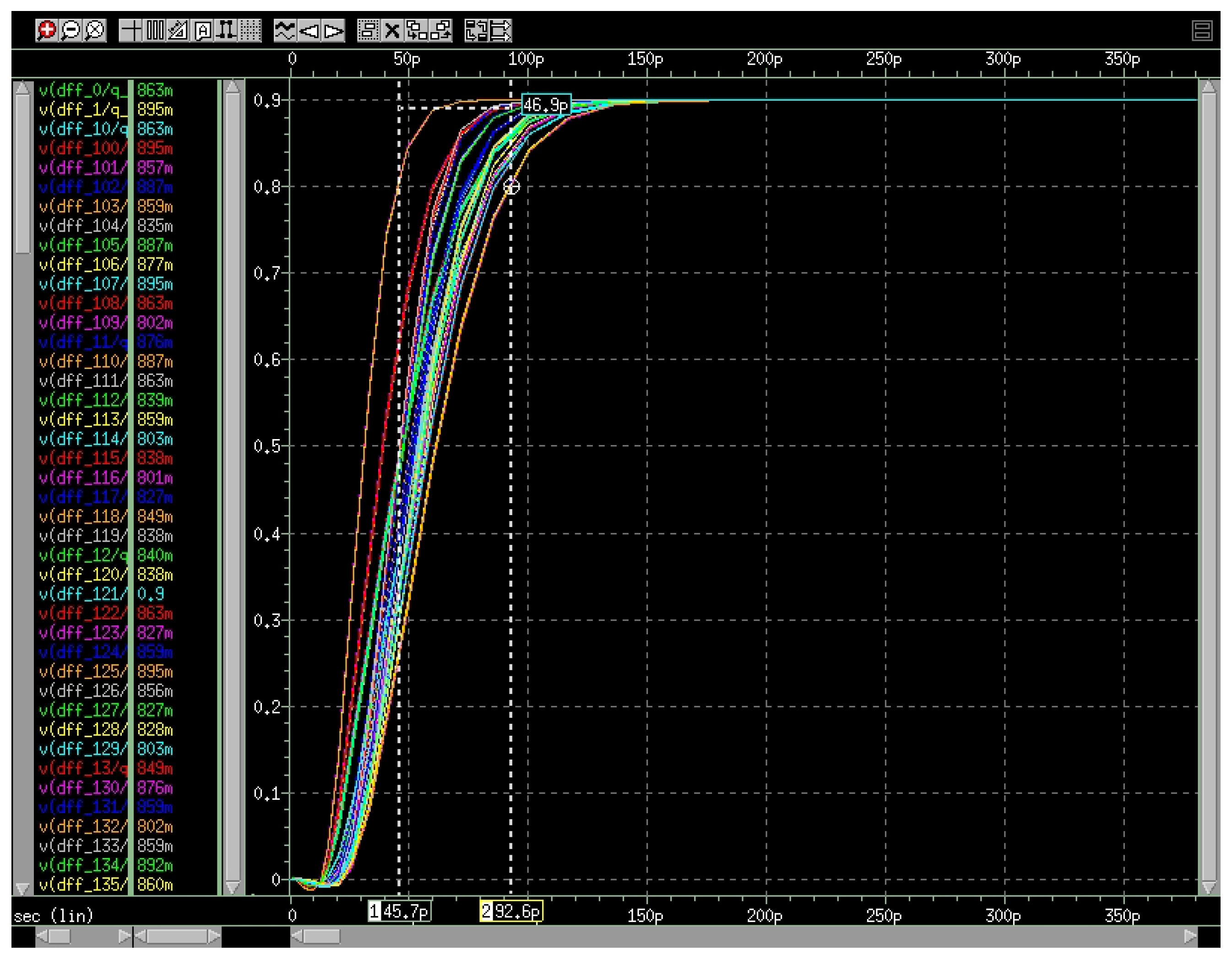
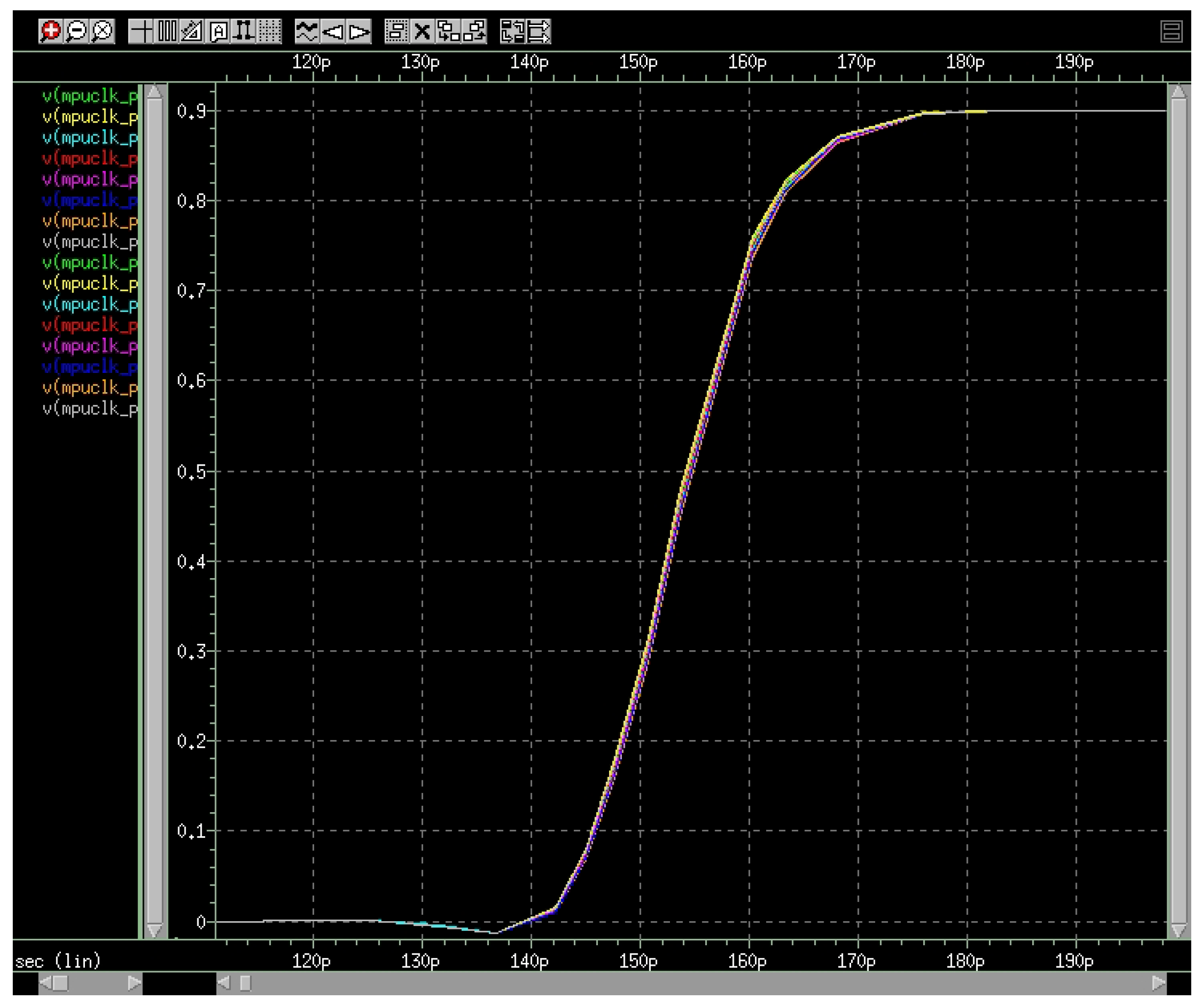
To be more consistent with clock mesh synthesis, we have also implemented our experiments with open-source benchmarks which have been synthesized by TSMC65nm in commercial EDA flow. Our design flow is developed in Python and Tcl language which can be integrated into current EDA tools. We have shown the results of ISCAS’89 and some VTR (Verilog To Routing) benchmarks in Table 2. The timing constraints of placed circuits are set according to the main frequency of 1.2GHz. For some comparisons, we have referenced some results from the work of [22] which used the same benchmarks as the original flow in Table 1. For experiments of the original flow, we select mesh grid sizing by iterations from a range which is from 4*4 to 200*200 based on engineering experience. Then, we use a larger selection scale of mesh width parameters from 2X to 6X to find the minimal penalty score which can satisfy hard constraints. Detailed SPICE simulations are applied to verify results. The slew constraint is 100ps for transition computation, and the skew constraint we have set is depending on the circuit scale. Finally, we can get the skew, power, and runtime values. For our proposed methodology, we have listed the optimal results for power consumption. The fine-tuning flow is able to converge to a low-skew solution within 2 to 3 iterations. The skew results are kept at the same level as the results of the original flow. The power consumption can be reduced up to an average 26.6% since the reduction of wire resources. The runtime measured by hours is also saved up to an average 78.0% because of the reduction of iterations. A layout example for benchmark circuit s35932 is shown in Figure 9 and Figure 10. Figure 9 is the clock mesh architecture designed, and Figure 10 is its routing graph including the pre-mesh tree, mesh wire resources, and post-mesh tree. The clock output response curve in Figure 11 also verifies the consistency of results, satisfying the 100ps slew constraint ( α = 50, β = 200, γ = 100). With tuning γ weight of the penalty score, a better skew result can also be achieved which is shown in Figure 12. This group of experiments corresponds to the data in Table 2 ( α = 50, β = 200, γ = 1000). Therefore, we can set weight values for different emphasis requirements, and the physical layout process also verifies the feasibility of the proposed methodology.
In order to further verify the effectiveness of the design method applied to the physical layout (IP modules that have been taped) [28,29,30], we conducted an experimental comparison with a commercial EDA tool flow, where the commercial EDA tool flow is a fully automatic clock tree synthesis method. Based on the proposed clock mesh design method, we optimized the experimental results through a fine-tuning hierarchical clock network. In Table 3, APE represents the name of the IP module, column C represents the commercial CTS(Clock Tree Synthesis) process, and column O represents the hierarchical clock network with optimized mesh methodology. The statistical results include the number of clock tree levels, the total number of buffers, WNS (Worst Negative Slack), TNS (Total Negative Slack), clock network latency, and power consumption. It should be pointed out that the OCV condition is 0.96/1.04 (representing the earliest and the latest delay attenuation rate). Under the worst corner condition, the clock buffer can be reduced by 61.1%, since the driving capability of the clock network is improved, and clock tree levels are reduced. The WNS can be increased by 240ps because of simpler buffer tree paths, and the TNS is also optimized. The clock network latency can be effectively controlled, and the power consumption can be optimized by 51.9%. In general, the clock mesh based on optimal design can combine effective hierarchical clock networks.
Table 2. Comparison between the original flow and our proposed methodology.
The original flow The proposed methodology
Benchmarks Grid
(M*N)
Wire width
(3X-5X)
Skew
(ps)
Power
(mW)
Runtime
(h)
Grid
(M*N)
Wire width
(2X-6X)
Skew
(ps)
Power
(mW)
Runtime
(h)
s13207 7*7 3X 8.3 49.3 1.2 6*6 4X 7.7 32.4 0.25
s15850 7*7 3X 4.2 42.2 1.8 5*5 4X 3.1 30.5 0.29
s35932 14*14 3X 19.3 137.2 2.2 10*10 4X 8.5 77.3 0.36
s38417 14*14 4X 16.7 127.3 2.5 11*7 5X 15.2 78.6 0.42
s38584 11*11 4X 15.2 118.3 1.9 8*6 5X 13.9 78.2 0.38
blob_merge 20*20 4X 22.1 253.7 3.5 18*14 5X 20.3 247.8 0.65
bmg 85*85 4X 27.5 425.6 5.3 64*54 5X 25.9 382.1 1.38
sha 16*16 4X 18.1 165.2 2.1 14*8 5X 17.3 93.6 0.51
stero2 120*120 4X 56.4 586.1 4.2 86*72 6X 46.5 421.6 1.67
ucsb 24*24 4X 25.5 279.4 2.8 19*16 5X 21.7 266.3 0.58
1664 microprocessor 155*135 4X 78.4 956.3 15.1 122*96 6X 66.1 718.6 3.2
8051 core 145*125 4X 69.4 853.1 14.2 118*92 6X 53.5 633.4 3.4
microprocessor za208 140*130 4X 62.3 821.1 13.9 101*82 5X 49.3 650.6 3.15
DarkRISCV 170*150 5X 87.9 962.7 21.5 158*126 6X 83.6 702.7 4.78
Neptune Core 185*140 5X 92.4 1075.1 26.0 172*120 6X 89.7 818.2 5.61
Table 3. Physical design experiments.
IP Module APE
Experiments C O
Clock tree levels 36 23
Total number of buffers 8952 3478
WNS(ns) -0.36 -0.12
TNS(ns) -925.7 -425.6
Clock network latency(ns) 1.85 1.64
Power consumption(mW) 1036.2 682.3

5. Conclusions

In this paper, we introduced a novel methodology for latency-bounded clock mesh synthesis, leveraging dynamic programming. Our experimental findings demonstrated the efficacy of our approach. We achieved a substantial reduction in power consumption, realizing an additional 26.6% reduction compared to the baseline. Furthermore, our methodology significantly improved runtime efficiency, saving an average of 78.0% compared to traditional simulation methods. As part of our future work, we aim to expand this framework to encompass irregular clock mesh designs, further advancing the applicability and versatility of our approach in addressing complex clock distribution challenges.

Author Contributions

Methodology, D.L. and M.L.; software, X.F., C.S. and Z.C.; original draft preparation, Q.C., W.P., L.Y., S.Q., X.J. and M.L.; review and editing, Q.C., Z.C. and M.L.; analysis and validation, D.L. and M.L. All authors have read and agreed to the published version of the manuscript.

Funding

This paper is funded by the project of the state grid corporation of China in 2020 “Integration Technology Research and Prototype Development for High End Controller Chip” (5700-202041264A-0-0-00) and Beijing Natural Science Foundation (No.4234089).

Data Availability Statement

Not Applicable.

Conflicts of Interest

Not Applicable.

References

  1. Restle, P.J.; McNamara, T.G.; Webber, D.A.; Camporese, P.J.; Eng, K.F.; Jenkins, K.A.; Allen, D.H.; Rohn, M.J.; Quaranta, M.P.; Boerstler, D.W.; et al. A clock distribution network for microprocessors. IEEE Journal of Solid-State Circuits 2001, 36, 792–799. [Google Scholar] [CrossRef]
  2. Maaz, M.; Bayoumi, M. A non-zero clock skew scheduling algorithm for high speed clock distribution network. In Proceedings of the 1999 IEEE International Symposium on Circuits and Systems (ISCAS), Vol. 6; 1999; pp. 382–385. [Google Scholar] [CrossRef]
  3. Andrew, B. Kahng, Jens Lienig, I.L.M.J.H. VLSI Physical Design: From Graph Partitioning to Timing Closure, 2022. [Google Scholar]
  4. Kanupriya Gulati, S.P.K. Hardware Acceleration of EDA Algorithms, 1 ed.; Springer New York, NY, 2010.
  5. Rajanish, K. Kamat, Santosh A. Shinde, P.K.G.H.G. Harnessing VLSI System Design with EDA Tools, 1 ed. Springer Dordrecht. 2011. [Google Scholar]
  6. Restle, P.; Carter, C.; Eckhardt, J.; Krauter, B.; McCredie, B.; Jenkins, K.; Weger, A.; Mule, A. The clock distribution of the POWER4 microprocessor. In Proceedings of the 2002 IEEE International Solid-State Circuits Conference. Digest of Technical Papers (Cat. No.02CH37315), Vol. 2; 2002; pp. 108–424. [Google Scholar] [CrossRef]
  7. Restle, P.; Franch, R.; James, N.; Huott, W.; Skergan, T.; Wilson, S.; Schwartz, N.; Clabes, J. Timing uncertainty measurements on the Power5 microprocessor. In Proceedings of the 2004 IEEE International Solid-State Circuits Conference (IEEE Cat. No.04CH37519); 2004. Vol.1.. pp. 354–355. [Google Scholar] [CrossRef]
  8. Thomson, M.; Restle, P.; James, N. A 5GHz Duty-Cycle Correcting Clock Distribution Network for the POWER6 Microprocessor. In Proceedings of the 2006 IEEE International Solid-State Circuits Conference - Digest of Technical Papers; 2006; pp. 1522–1529. [Google Scholar] [CrossRef]
  9. Wendel, D.F.; Kalla, R.; Warnock, J.; Cargnoni, R.; Chu, S.G.; Clabes, J.G.; Dreps, D.; Hrusecky, D.; Friedrich, J.; Islam, S.; et al. POWER7™, a Highly Parallel, Scalable Multi-Core High End Server Processor. IEEE Journal of Solid-State Circuits 2011, 46, 145–161. [Google Scholar] [CrossRef]
  10. Restle, P.; Shan, D.; Hogenmiller, D.; Kim, Y.; Drake, A.; Hibbeler, J.; Bucelot, T.; Still, G.; Jenkins, K.; Friedrich, J. 53 Wide-frequency-range resonant clock with on-the-fly mode changing for the POWER8TM microprocessor. In Proceedings of the 2014 IEEE International Solid-State Circuits Conference Digest of Technical Papers (ISSCC); 2014; pp. 100–101. [Google Scholar] [CrossRef]
  11. Heald, R.; Aingaran, K.; Amir, C.; Ang, M.; Boland, M.; Das, A.; Dixit, P.; Gouldsberry, G.; Hart, J.; Horel, T.; et al. Implementation of a 3rd-generation SPARC V9 64 b microprocessor. In Proceedings of the 2000 IEEE International Solid-State Circuits Conference. Digest of Technical Papers (Cat. No. 00CH37056). IEEE; 2000; pp. 412–413. [Google Scholar]
  12. Wendell, D.; Lin, J.; Kaushik, P.; Seshadri, S.; Wang, A.; Sundararaman, V.; Wang, P.; McIntyre, H.; Kim, S.; Hsu, W.; Park, H.; Levinsky, G.; Lu, J.; Chirania, M.; Heald, R.; Lazar, P. A 4MB on-chip L2 cache for a 90nm 1. In 6GHz 64b SPARC microprocessor. In Proceedings of the 2004 IEEE International Solid-State Circuits Conference (IEEE Cat. No.04CH37519); 2004. Vol.1. pp. 66–513. [Google Scholar] [CrossRef]
  13. Northrop, G.; Averill, R.; Barkley, K.; Carey, S.; Chan, Y.; Chan, Y.; Check, M.; Hoffman, D.; Huott, W.; Krumm, B. ; others. In 609 MHz G5 S/399 microprocessor. In Proceedings of the 1999 IEEE International Solid-State Circuits Conference. Digest of Technical Papers. ISSCC. First Edition (Cat. No. 99CH36278). IEEE; 1999; pp. 88–89. [Google Scholar]
  14. Rajaram, A.; Pan, D.Z. MeshWorks: An efficient framework for planning, synthesis and optimization of clock mesh networks. In Proceedings of the 2008 Asia and South Pacific Design Automation Conference. IEEE; 2008; pp. 250–257. [Google Scholar]
  15. Rajaram, A.; Pan, D.Z. MeshWorks: A Comprehensive Framework for Optimized Clock Mesh Network Synthesis. IEEE Transactions on Computer-Aided Design of Integrated Circuits and Systems 2010, 29, 1945–1958. [Google Scholar] [CrossRef]
  16. Cho, M.; Pan, D.Z.; Puri, R. Novel binary linear programming for high performance clock mesh synthesis. In Proceedings of the 2010 IEEE/ACM International Conference on Computer-Aided Design (ICCAD). IEEE; 2010; pp. 438–443. [Google Scholar]
  17. Abdelhadi, A.; Ginosar, R.; Kolodny, A.; Friedman, E.G. Timing-driven variation-aware nonuniform clock mesh synthesis. In Proceedings of the 20th symposium on Great lakes symposium on VLSI; 2010; pp. 15–20. [Google Scholar]
  18. Guthaus, M.R.; Wilke, G.; Reis, R. Non-uniform clock mesh optimization with linear programming buffer insertion. In Proceedings of the 47th Design Automation Conference; 2010; pp. 74–79. [Google Scholar]
  19. Sitik, C.; Taskin, B. Multi-voltage domain clock mesh design. In Proceedings of the 2012 IEEE 30th International Conference on Computer Design (ICCD). IEEE; 2012; pp. 201–206. [Google Scholar]
  20. Lu, J.; Mao, X.; Taskin, B. Timing slack aware incremental register placement with non-uniform grid generation for clock mesh synthesis. In Proceedings of the 2011 international symposium on Physical design; 2011; pp. 131–138. [Google Scholar]
  21. Teng, Y.; Taskin, B. Clock mesh synthesis method using the Earth Mover’s Distance under transformations. In Proceedings of the 2012 IEEE 30th International Conference on Computer Design (ICCD); 2012; pp. 121–126. [Google Scholar] [CrossRef]
  22. Lu, J.; Mao, X.; Taskin, B. Clock mesh synthesis with gated local trees and activity driven register clustering. In Proceedings of the 2012 IEEE/ACM International Conference on Computer-Aided Design (ICCAD). IEEE; 2012; pp. 691–697. [Google Scholar]
  23. Liu, W.H.; Li, Y.L.; Chen, H.C. Minimizing clock latency range in robust clock tree synthesis. In Proceedings of the 2010 15th Asia and South Pacific Design Automation Conference (ASP-DAC). IEEE; 2010; pp. 389–394. [Google Scholar]
  24. Ewetz, R.; Tan, C.Y.; Koh, C.K. Construction of latency-bounded clock trees. In Proceedings of the 2016 on International Symposium on Physical Design; 2016; pp. 81–88. [Google Scholar]
  25. Chen, H.; Yeh, C.; Wilke, G.; Reddy, S.; Nguyen, H.; Walker, W.; Murgai, R. A sliding window scheme for accurate clock mesh analysis. In Proceedings of the ICCAD-2005. IEEE/ACM International Conference on Computer-Aided Design, 2005, IEEE; 2005. pp. 939–946. [Google Scholar]
  26. Sze, C.N. ISPD 2010 high performance clock network synthesis contest: Benchmark suite and results. In Proceedings of the 19th international symposium on Physical design; 2010; pp. 143–143. [Google Scholar]
  27. Guthaus, M.R.; Hu, X.; Wilke, G.; Flach, G.; Reis, R. High-performance clock mesh optimization. ACM Transactions on Design Automation of Electronic Systems (TODAES) 2012, 17, 1–17. [Google Scholar] [CrossRef]
  28. Liu, M.; Zhang, Z.; Sun, W.; Wang, D. A novel obstacle-aware multiple fan-out symmetrical clock tree synthesis. IEICE Electronics Express 2017, 14, 20170935–20170935. [Google Scholar] [CrossRef]
  29. Zhang, Z.; Liu, M.; Liu, Z.; Du, X.; Xie, S.; Ma, H.; Ding, G.; Ren, W.; Zhou, F.; Sun, W.; et al. Progress in a novel architecture for high performance processing. Japanese Journal of Applied Physics 2018, 57, 04FA03. [Google Scholar] [CrossRef]
  30. Liu, M. A co-design method of customized ISA design space exploration and fixed-point library construction for RISC-V dedicated processor. IEICE Electronics Express 2022, 19, 20220244–20220244. [Google Scholar] [CrossRef]
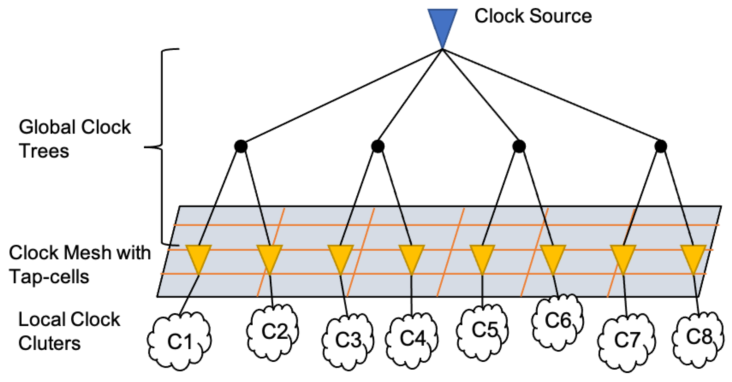
Figure 1. The clock mesh structure.
Preprints 84674 g001
Figure 2. The clock mesh track details.
Preprints 84674 g002
Figure 3. The proposed clock mesh synthesis methodology.
Preprints 84674 g003
Figure 4. The mesh window model to estimate the latency.
Preprints 84674 g004
Figure 5. An interconnect of length l with the uniform width w.
Preprints 84674 g005
Figure 6. The one-segment RC model for the interconnect.
Preprints 84674 g006
Figure 7. The mesh planning state example. The orange rectangle represents the mesh window with M p a t t e r n 2 , 3 which is 2 rows and 3 columns. The blue rectangle represents the redundant area of the layout. Grey lines represent mesh routing tracks, and grey triangles represent clocks buffers. Green rectangles represent the key sink for each mesh window. The blue arrows indicate the maximum and minimum latency values in Manhattan space.
Preprints 84674 g007
Figure 8. The clock grid zone removal.
Preprints 84674 g008
Figure 9. The clock mesh layout.
Preprints 84674 g009
Figure 10. The clock mesh layout after routing.
Preprints 84674 g010
Figure 11. The clock mesh output response curve with γ = 100 .
Preprints 84674 g011
Figure 12. The clock mesh output response curve with γ = 1000 .
Preprints 84674 g012
Table 1. Results for ISPD2010 benchmarks.
BM. Sinks LAT.
(ps)
Grid
(M*N)
SC Area
RD.
Run.0
(min)
Run.1
(min)
01 1107 20 27*18 12.5 8.3% 56 27
02 2249 20 38*21 27.9 12.5% 101 50
03 1200 20 16*12 16.2 9.7% 9 4
04 1845 20 17*18 25.1 10.3% 31 14
05 1016 10 14*12 8.3 9.2% 18 8
06 981 10 13*12 7.2 7.8% 15 6
07 1915 20 22*13 24.6 11.2% 27 13
08 1134 10 14*15 9.1 8.9 % 8 4
Disclaimer/Publisher’s Note: The statements, opinions and data contained in all publications are solely those of the individual author(s) and contributor(s) and not of MDPI and/or the editor(s). MDPI and/or the editor(s) disclaim responsibility for any injury to people or property resulting from any ideas, methods, instructions or products referred to in the content.
Copyright: This open access article is published under a Creative Commons CC BY 4.0 license, which permit the free download, distribution, and reuse, provided that the author and preprint are cited in any reuse.
Prerpints.org logo

Preprints.org is a free preprint server supported by MDPI in Basel, Switzerland.

Subscribe

© 2024 MDPI (Basel, Switzerland) unless otherwise stated