1. Introduction
Silicon carbide semiconductor, known for its robustness and chemical resistance, is broadly applied across diverse industries such as electronics, automotive, aerospace, and power generation. The research is focused on the cubic form of silicon carbide, 3C-SiC (β-SiC), which exhibits a zinc-blende structure with uniform bond lengths. This arrangement is the product of two interconnected face-centered cubic lattices, offset along the diagonal by a quarter of its length[
1]. Both, composition and high binding energy results in exceptional stability and unique properties. These include hardness, superior thermal conductivity, resistance to radiation and high temperatures, all of which makes it suitable for deployment in extreme conditions like those found in fusion[
2] and fission reactors[
3]. For instance, it serves as a shielding material in TRISO fuel[
4]. Furthermore, SiC should be also the main construction material of the new generation of high temperature nuclear reactors such as the Dual Fluid Reactor[
5]. In this reactor, liquid uranium-chromium eutectic will be used as fuel which will flow through a large number of closely placed SiC tubes. Liquid lead is expected to act as a coolant that flows along the SiC tubes and removes the produced heat from the reactor core. Thus, the corrosive interaction between liquid metals and SiC ceramics under irradiation of high energy neutrons will likely be one of the most important limiting factors, deciding about success of future reactor constructions – see also a similar design of the heat pipe microreactor[
6].
Utilizing first-principles methods to observe shifts in electronic factors that dictate bond formation and breakage allows for the determination of adsorption energies, investigation of reaction mechanisms and resulting structural changes. It has been recently[
7] shown that the density functional theory can provide corrosion indicators of chosen ceramic materials such as adsorption energy of corrosive atoms and corresponding charge density differences predicting experimental results. Similar studies have not been performed on 3C-SiC, so far. On the other hand, the exploration of interactions between lead and silicon carbide may hold significant implications for various domains. These include besides the corrosion science also material science and nanotechnology[
8] as well as less obvious areas such as lead detection and removal[
9].
The study investigated the adsorption of lead atoms on three different reconstructed[
10] 3C-SiC surfaces (100, 110, 111), with either carbon or silicon terminations. Tests were implemented for various monolayer (ML) coverages.
2. Method
The present study employs a computational methodology based on Density Functional Theory (DFT), implemented in the Plane-Wave Self-Consistent Field (PWscf) programs, a component of the Quantum ESPRESSO – open source software for quantum computations[
11,
12].
The pseudopotentials employed[
13] are based on the Projector Augmented-Wave (PAW) method. The electron exchange-correlation effects were treated within the generalized gradient approximation (GGA) utilizing the Perdew-Burke-Ernzerhof (PBE)[
14] exchange-correlation functional. For all calculations, the energy cutoff was set to 350 Ry. The lead potential was generated using fully relativistic calculations, while other potentials were generated with Scalar-Relativistic Calculations.
The lattice parameter was determined using Birch–Murnaghan isothermal equation of state[
15] for a periodically replicated single cell. The calculated constant (4.379Å) aligns with the simulation[
16] and the experimental results[
17] (4.348Å), which were subsequently used to create the adsorption models[
18]. All simulations utilized periodic boundaries to create a slab model, integrating a vacuum region of 12Å in the z-direction to reduce interactions with the image of the next slab's underside.
Truncation of the crystal's bulk structure results in the appearance of unbalanced forces acting upon the atoms. Surface reconstructions were executed to locate their new equilibrium positions. To ensure a proper transition to the bulk crystal, the two lowermost layers were fixed to the bulk coordinates. The dangling bonds of the bottom surface were saturated with hydrogen atoms, which were fixed in the obtained positions in the adsorption calculations. Relaxations were conducted until the forces acting on atoms were below 0.02eV/Å.
Various coverages were examined by placing a lead adatoms on supercells composed of 2x2 and 3x3 cells. These configurations correspond to a monolayer (ML) coverage of 1/4 and 1/9 ML. Due to the importance of the mutual interaction between lead atoms at higher atomic packing, investigations were conducted on configurations with two or more lead atoms on a 2x2 supercell, which corresponds to 1/2 ML, 3/4 ML and 1 ML.
For the integration of the Brillouin zone, k-point samplings of 6x6x1, 3x3x1 Monkhorst-Pack grids was applied, accordingly, for other cases they were proportionally adjusted. High-symmetry adsorption sites (as applicable) were considered: T on top, B bridge, SB short bridge, LB long bridge, H hollow: in 110 surface over atom and in 111 fcc over atom in lower layer, hcp over hollow site. In post processing, the charge density difference (CDD) was determined and the charge transfer from lead to the SiC surface was analyzed using Bader charge analysis[
19].
The adsorption energy E
Ad is defined by the following equation:
where
ESiC+Pb is the total energy of a slab with an adsorbed lead atom,
ESiC is the energy of the clean slab,
EPb is the energy of an isolated lead atom.
N denotes the number of adatoms. CDD describes the disparity between the charge density of a system and a reference configuration and adatom[
20]. With this method, alterations in charge distribution can be visually represented.
3. Results
3.1. 100. surface
The 100 supercells consist of eight layers of atoms – four carbon, three silicon for the C-rich surface and vice versa for the Si-rich surface. Both scenarios include a stabilizing hydrogen layer at the base. In order to facilitate simulation of formation of atomic pairs (dimers) during surface reconstruction the samples were rotated by 45
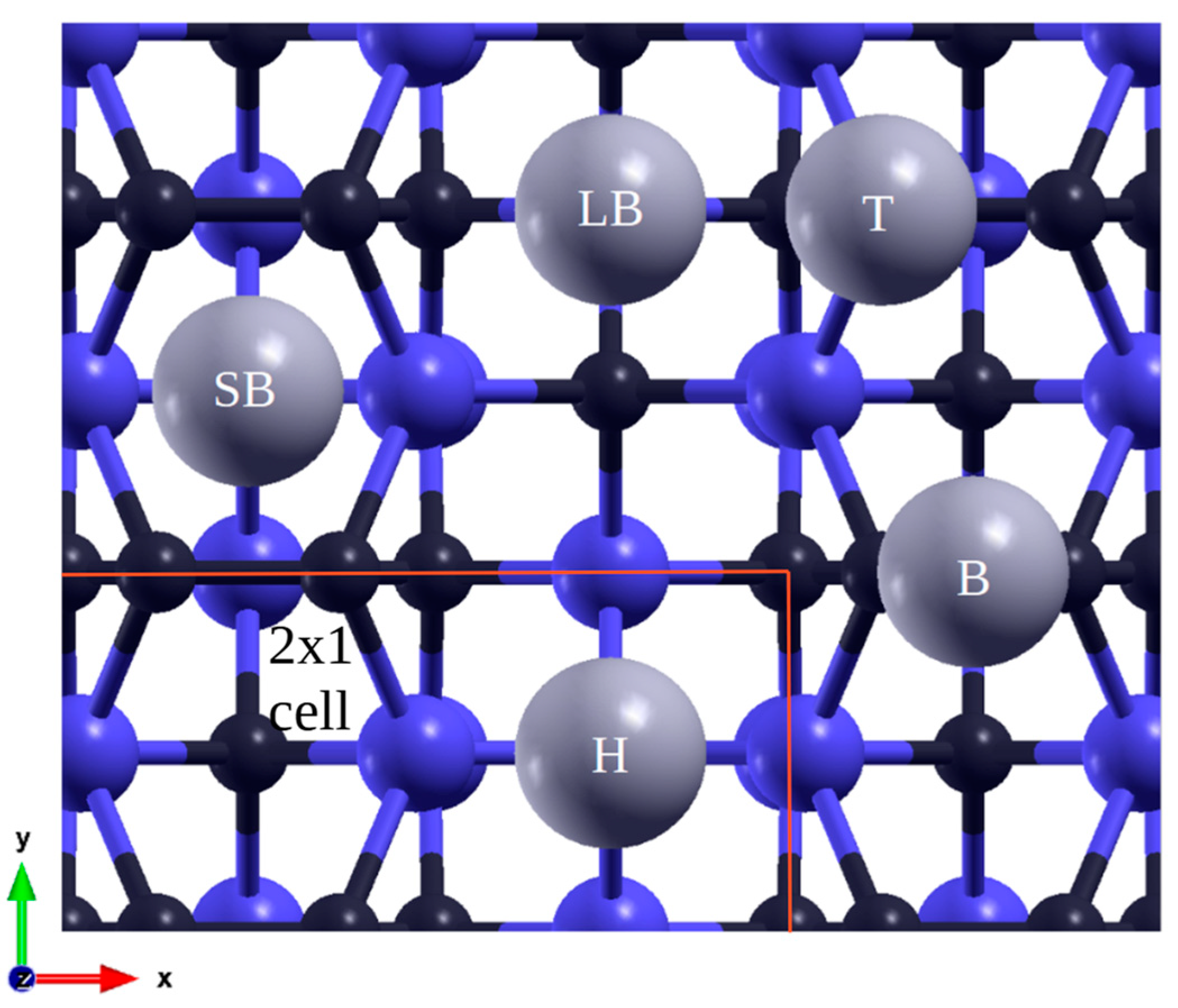
o along the z-axis, resulting in an arrangement as shown in
Figure 1. This adjustment does not impact the surface, only simplifies calculations. While there exist multiple possible configurations[
1], the linearly arranged dimers were reproduced in the case of the C – terminated (100) surface[
21]. The formation of dimers reduces the number of dangling bonds and disrupts symmetries, hence the smallest periodic space is composed of two cells in a 2x1 configuration. Consequently, coverages of 1/2, 1/4, and 1/16 ML were calculated for this case. The boundaries and adsorption sites are marked in
Figure 1.
The derived carbon-carbon bond length is 1.374 Å, aligning closely with another study's findings[
22] (1.36). The on-top position was found to be unstable for all ML and transitioned to the bridge position. The short bridge position emerged as the most energetically favored with an average bond length of 2.47 Å and a donation of 0.89 electron, which is the maximum among all the tested values. The results obtained are presented in
Table 1. In the test 1/2 ML with two atoms, the adatoms settled in positions of the bridge and non-adjacent long bridge but were not exactly aligned. A slight tilting led to a reduction in the distance between them, which measure 3.25 Å. Thus, the atoms form rows rather than a uniform lattice. The resulting energy is -2.16 eV per atom, it is very close to the LB value for 1/4 ML, the bond lengths are slightly shorter than in that case and are 2.35 Å and 2.43 Å, respectively.
For the Si-rich 100 surface, the initial position was the ideal surface geometry. Considering the small energy difference from the configuration with dimers[
23], this configuration was retained for further calculations after relaxation, during which the atoms moved solely vertically. For improved comparison, the 1/16 ML case was also computed. The atop site is unstable in 1/16 ML and similarly the SB position has the lowest energy and forms bond 2.92 Å long, with 0.33 charge transfer. Due to the symmetry of the relaxed lattice, here SB is equivalent to H. The obtained results are shown in
Table 2.
In the tests involving two atoms, the adatoms, due to repulsion, shifted to the bridge positions, establishing an alternating rows arrangement and staying at the same height. The obtained energy per atom was -2.24 eV which is lower, from the cases of 1/4 ML. Probably due to the occupation of the second, free bridge position in the cell. The bond length with silicon was 2.78 Å for both instances. The final case 3/4 ML resulted in the formation of two layers of lead for both cases therefore, further tests were not conducted. The stable positions were as for the previous case with the second layer atom in the center of the arising square. The bond lengths are similar, but the deviations in the positions of the atoms on the surface are smaller. Thus, for this surfaces, the saturated monolayer coverage will be somewhere between 1/2 and 3/4 ML.
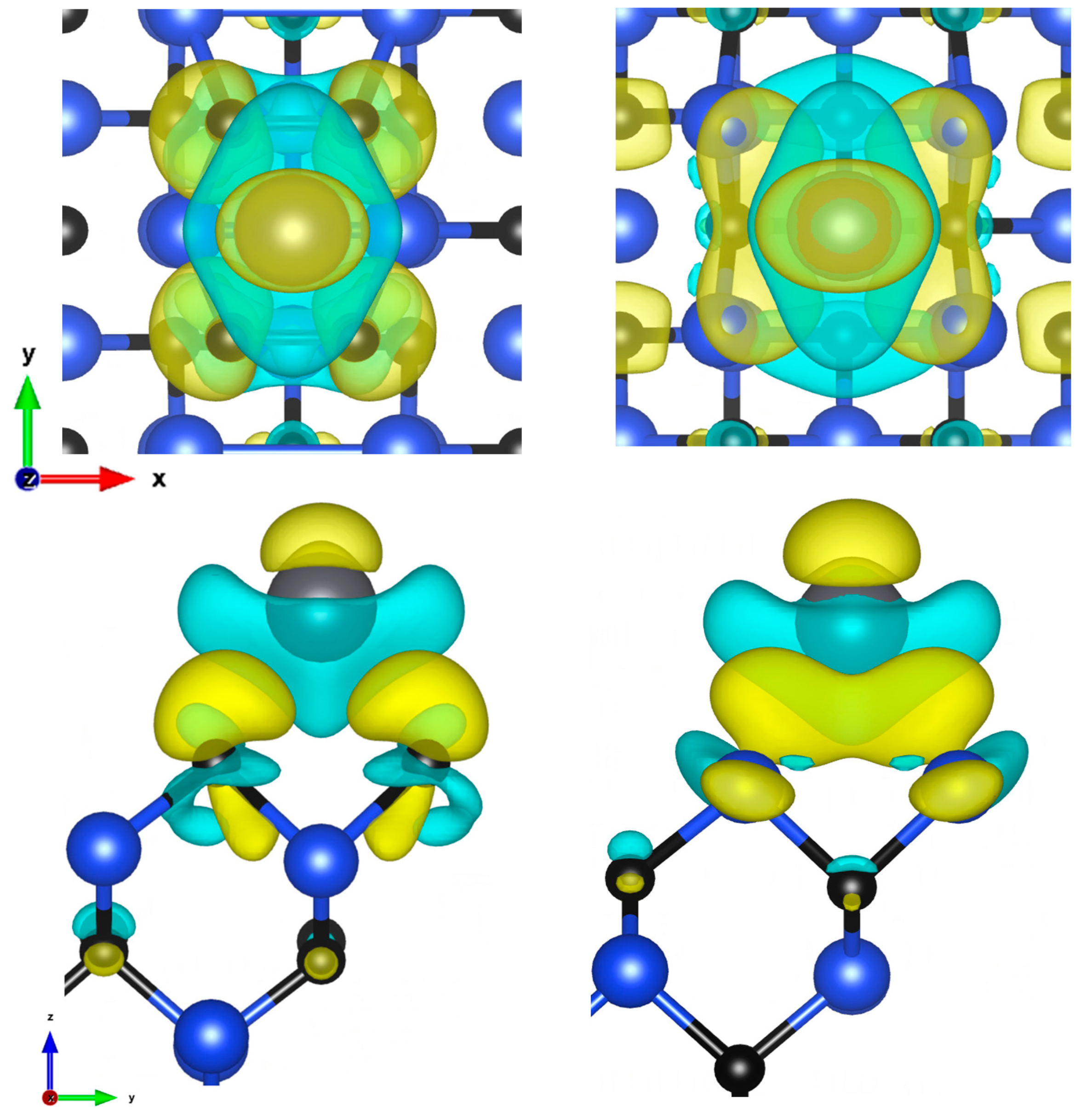
In
Figure 2 and the rest of the CDD of the graphs, the yellow color indicates the spaces in which the charge density has increased and the blue color in which it has decreased. The charge is transferred to the neighboring carbon and silicon atoms, respectively. There is also a small transfer to the over atom and also to the carbon atoms in the layers below.
3.2. 110. surface
The surface made by face diagonal plane (110) is nonpolar and low-index. During the relaxation process, silicon atoms, as anticipated from materials with a similar structure, underwent both vertical and horizontal displacements, moving inward in the structure, while the C atoms positions remained almost unchanged[
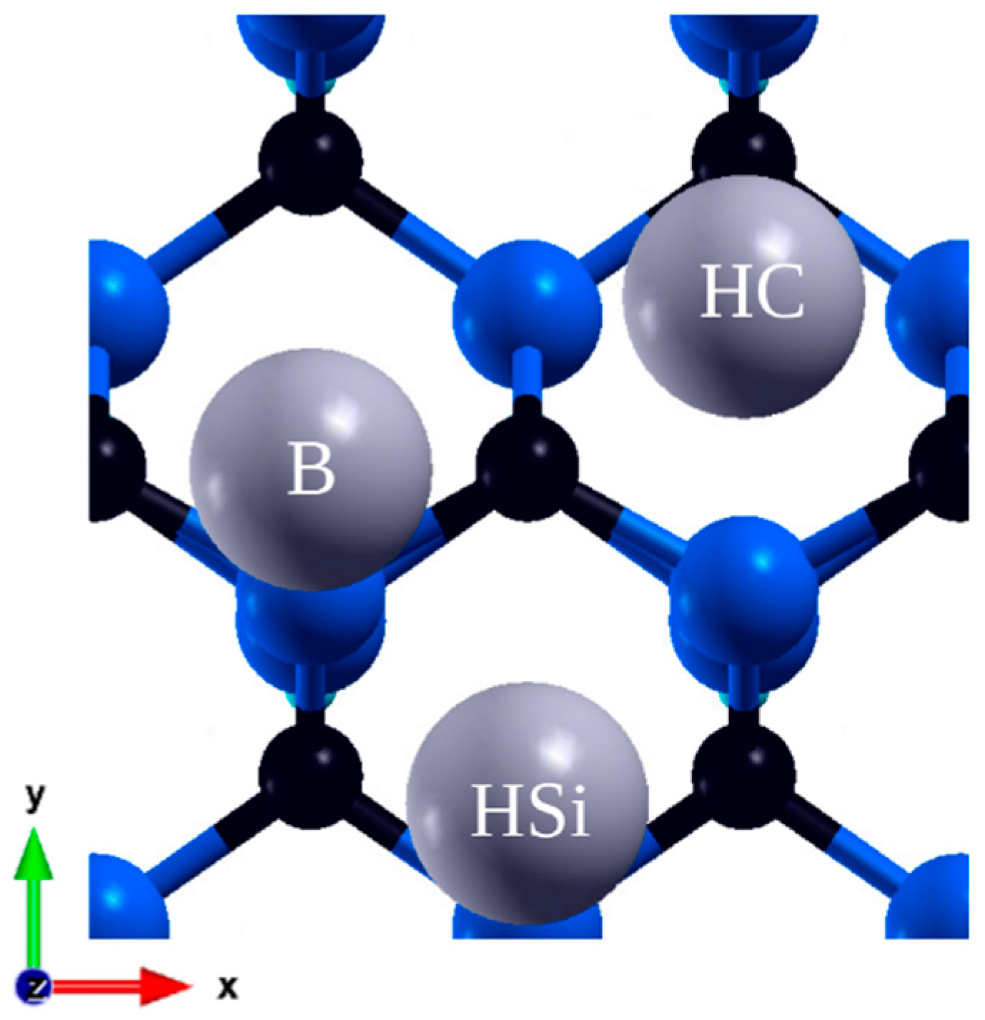
22]. A single cell contains two atoms on the surface, thus yielding smaller coverages of 1/4, 1/8 i 1/18 ML. This simulation space consisted of six layers of atoms and a hydrogen layer. In these calculations there are two hollow sites, which almost overlap with an atom from the layer below, one being over Si and the second over C, as depicted in
Figure 3. These two positions are the most stable, while others – the bridge, on top of Si and C – are unstable. The exception is the positions on the bridge in 1/8 ML. However, in the latter case, the atom did not retain its original position but moved to a new, unanticipated yet stable position (B) with an energy of -1.54 eV. This value is considerably smaller than the others so, given the instability of the other sites, it is plausible that after a significant increase in accuracy, it would have moved to the prevailing minima, too.
Table 3.
Adsorption energies in eV for 110 surface.
Table 3.
Adsorption energies in eV for 110 surface.
| Adsorption sites |
1/18 ML |
1/8 ML |
1/4 ML |
3/8 ML |
1/2 ML |
| Hollow Si (HSi) |
-2.05 |
-1.99 |
|
|
|
| Hollow C (HC) |
-2.36 |
-2.34 |
-2.81 |
-2.46 |
-2.34 |
For the Hollow C site, lead donates 0.48 electrons, indicating a significant contribution from covalent bonding. Three bonds are formed with lengths of 2.63 Å for two carbon atoms and 2.76 Å for silicon atom. In a simulation of 1/4 ML coverage, adatoms occupy HC positions forming an alternating line. The adsorption energy is less than for other coverages also in case of 100 surface. Bond lengths are shorter and are equal to 2.58 Å for C atoms and 2.75 Å for Si. In the next larger overlap, another vacant HC position was filled, directly next to the already occupied one, due to this short distance and adatom interaction, the adsorption energy increased. For the row of atoms thus formed, the distance from the C atoms increased to 2.83 and slightly to Si, the third atom remained almost unchanged. Only in this case, in a simulation with four adatoms, all of them remained on the surface. An additional atom also occupied the HC position, and affected the atom directly next to it, similarly increasing its distance to the surface.
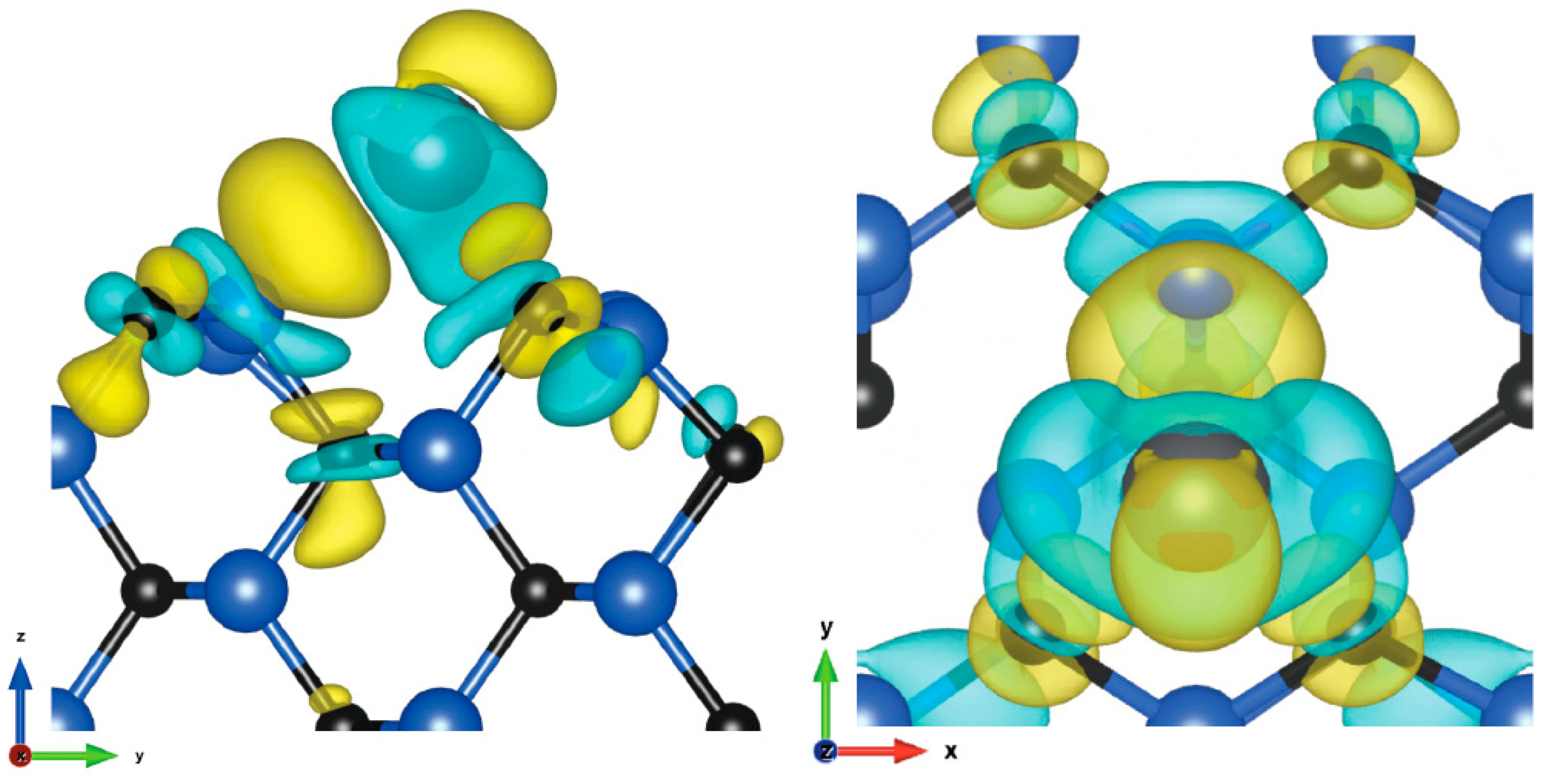
Figure 4.
Charge density difference visualization of 110 plane 1/4 ML, Hollow C site, side and top view (isosurface value: 2.2 me/Å3).
Figure 4.
Charge density difference visualization of 110 plane 1/4 ML, Hollow C site, side and top view (isosurface value: 2.2 me/Å3).
In this case, the charge is mainly transferred to the nearest silicon atom from which it is partially transferred to its neighboring carbon atoms, and also to a lesser extent above the atom. Much less charge is transferred to the nearest carbon atoms because it is split between two of them.
3.3. 111. surface
The final structure studied, with the surface formed by the body diagonal plane (111), consisted of nine atomic layers. This surface occurs in two types with either one or three dangling bonds per atom on the surface, here the first case is discussed. The supercell was reconstructed using a hexagonal cell. Although this arrangement resembles the α-SiC (0001)[
7,
24,
25] surface, it has a different electronic structure which affects the length of the bonds to next layer. Due to the hexagonal symmetries, only vertical displacements were observed in both preparation and adsorption studies. The investigation covered three sites: on top, face-centered cubic (fcc) hollow, and hexagonal close-packed (hcp) hollow (over an atom from a deeper layer), all of which proved to be local minima.
For the C-face 111 surface, the, the hcp site, also the lowest of all obtained results, exhibited bonds of 2.52 Å with carbon. During the reaction 0.82 electrons were exchanged. In both instances, the energies for the other hollow site were very close, differing by approximately 0.1 eV. In tests involving two atoms at 1/2 ML, the lead formed a honeycomb lattice, with atoms in on-top and hcp positions. The bond lengths were 2.29 Å and 2.57 Å, respectively, close to the values for 1/4 ML. The mean Pb-Pb distance was 3.52 Å. In the 3/4 ML, the atoms stabilized at the hcp, fcc and on top positions, forming a hexagonal lattice with a similar mean distance of 3.55 Å between lead atoms. Among tests, for the 111 Si-face surface, the fcc site demonstrated the highest adsorption with a mean silicon bond length of 2.84 Å. However, there was a transfer of only 0.18 electrons, indicating a more covalent nature of the bond. For 1/2 ML, the same arrangement was formed and the atoms occupied the same adsorption sites with bond lengths of 2.76 Å and 2.94 Å, respectively. The resulting distance between the lead atoms is 3.56 Å. The derived adsorption energies are very close to the corresponding average energy of these positions from 1/4 ML, for both instances. In the 3/4 ML, during relaxation the atoms passed through the same regular position, which in this case turned out to be semistable. The final lattice consists of deviated two positions on top and bridge to form a less regular but single hexagonal layer, with distances ranging from 3.3 to 4.04 Å, with an average of 3.57 Å. The final 1 ML test resulted in a second layer of lead atoms in both cases. The three atoms on the surface occupied the same positions as for the 3/4 ML coverage, proving that the maximum monolayer coverage is between 3/4 and 1 ML.
The CDD diagram obtained is almost identical to that presented in the detailed study of the SiC(0001) surface in [
7] for the two outer layers of atoms. Also, the adsorption energies obtained are similar and show a comparable increasing trend, also the Si-terminated surface shows higher energies.
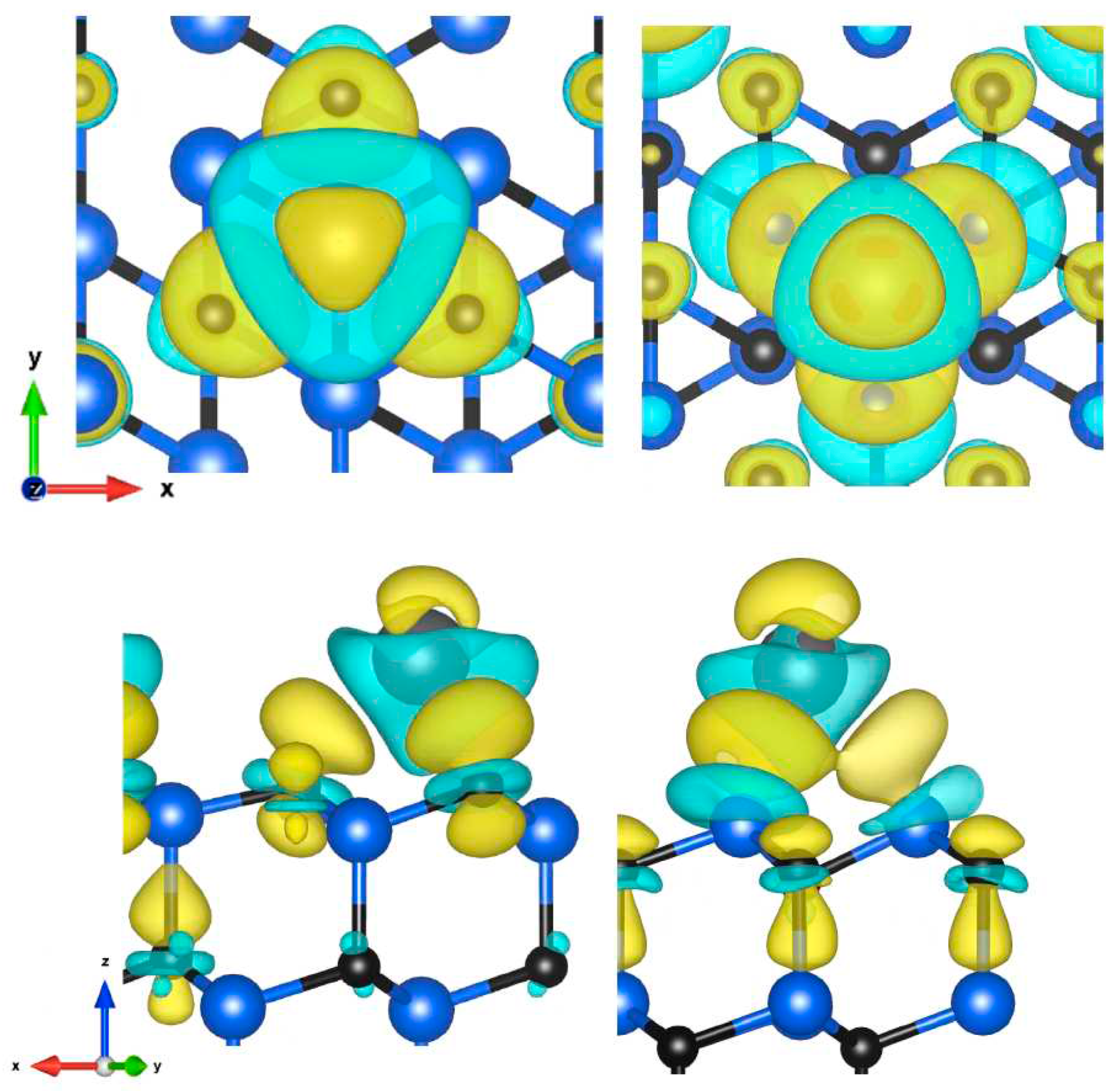
Figure 5.
Charge density difference visualization of C-face (hcp) and Si-face (fcc) sites of 111 plane, top and side view (isosurfaces values: 2.4 and 1.6 me/Å3).
Figure 5.
Charge density difference visualization of C-face (hcp) and Si-face (fcc) sites of 111 plane, top and side view (isosurfaces values: 2.4 and 1.6 me/Å3).
In C-face, the transferred charge accumulates mainly around the nearest carbon atoms but also around the carbon atom of the lower layer farther from the adatoms, and to a lesser extent directly above the atom. In the second case, the charge is transferred to neighboring silicon atoms from where it spreads to the carbon atoms below. A small fraction is also located above the atom.
Table 4.
Adsorption energies in eV for C-terminated 111 surface.
Table 4.
Adsorption energies in eV for C-terminated 111 surface.
| Adsorption sites |
1/9 ML |
1/4 ML |
1/2 ML |
3/4 ML |
1 ML |
| Top (T) |
-2.65 |
-2.56 |
-3.02 |
-2.72 |
-2.39 |
| fcc-Hollow |
-3.51 |
-3.39 |
|
-2.72 |
-2.39 |
| hcp-Hollow |
-3.64 |
-3.59 |
-3.02 |
-2.72 |
-2.39 |
Table 5.
Adsorption energies in eV for Si-terminated 111 surface.
Table 5.
Adsorption energies in eV for Si-terminated 111 surface.
| Adsorption sites |
1/9 ML |
1/4 ML |
1/2 ML |
3/4 ML |
1 ML |
| Top (T) |
-2.71 |
-2.43 |
-2.93 |
-2.77 |
-2.36 |
| fcc - Hollow |
-3.6 |
-3.53 |
|
|
|
| hcp - Hollow |
-3.49 |
-3.45 |
-2.93 |
-2.77 |
-2.36 |
4. Discussion
The adsorption of lead was examined on three representative 3C-SiC surfaces with different coverage levels. Our findings revealed that only a subset of the probed positions exhibit stability. Additionally, a previously unidentified adsorption position was discovered. No studies have been identified specifically addressing the adsorption of Pb on 3C-SiC. Instead, more attention has been directed towards the intercalation of this metal either on or beneath a graphene layer on SiC[26, 27], driven by the potential to modify its properties through spin-orbit coupling. Research on 6H and 4H-SiC[
7,
28,
29] also attracts attention due to their simpler production processes and greater availability. Unfortunately, the differences in configurations allows only for approximate comparisons of trends. Referring to [
28], where a single SiC layer was explored, the bond length with Si (2.835 Å) closely aligns with our recorded value (2.84 Å) for a corresponding hcp position on the Si-face 111. Notably, the energy in this context is significantly lower, a variation likely attributable to charge transfer extending to deeper layers. This bond length is also consistent with the (2.79 Å) measurement from [
28] for the surface of 6H-SiC, and similarly for the fcc site.
The binding energies for all examined positions suggest chemisorption. It is observed that as coverage increases, the binding energy typically rises as a result of adatom interactions, which can be observed especially for cases with smaller distances between adsorption sites. The exceptions are the cases of 100 for 1/2 ML coverage and 110 for higher coverages, which can be explained by the occupation of successive low-energy positions that are, however, enough distant to have little effect on the neighboring adatom. Importantly, no reactions leading to Si-C or C-C bond breakage were observed. This pattern may explain the generally weak interaction observed at the macroscale[
31,
32], where minimal or no response has been reported. As can be observed from the Charge Density Difference graphs, in all cases the lead atom transfers charge to the lattice, which predominantly accumulate around carbon atoms. This is due to the fact that carbon has the highest electronegativity of 2.52 among the atoms in the simulation, compared to 1.82 for silicon and 1.56 for lead[
33]. Consequently, in configurations where a bond with carbon exists, a larger charge transfer from lead is observed, in most cases resulting in a relatively higher binding energy, silicon in the crystal further enhances this effect[
34]. The explored cases of 1/2 ML and higher – an adsorption involving two or more lead atoms, as opposed to one[
35], underscore the significance of Pb-Pb interaction. Owing to this interaction, the most energetically favorable positions could be two distinct positions or their slight distortion, rather than stable positions in isolation, which cannot be studied with a single atom. The strongest bonds formed on the 111 surface at hcp-hollow site, where three bonds with carbon atoms yielded an energy of -3.64 eV. For the other instances, considering the lowest coverage, where by a large distance Pb-Pb interactions are minimal, these include the fcc-hollow position for 111 with an energy of -3.6 eV, hollow C for 110 with an energy of -2.36 eV, and the short bridge for both 100 surfaces, with -2.33 and -2.53 eV respectively. This pattern shows that the adsorption energy is a result of the specific arrangement of and atoms exposed to interactions and their neighbors rather than just their surface energies[
36]. Carbon attracts electrons more strongly, while silicon can transfer charges to three more carbon atoms, which is clearly visible in the case of 110. The lower binding energy in 100 C-face is caused by the formation of dimers which result in a reduced number of dangling bonds. The results show that positions where there is interaction with one or two dangling bonds are much weaker or unstable, as opposed to stable positions held by three or four such bonds.
Acknowledgments
This work was supported by the Polish National Research and Development Center (NCBR) project “New Reactor Concepts and Safety Analyses for the Polish Nuclear Energy Program”, POWR.03.02.00-00-I005/17 (years 2018–2023). Calculations were performed on a computer cluster of Świerk Computer Center (CIŚ).
References
- V. Y. Aristov "β-SiC(100) surface: atomic structures and electronic properties”. Physics-Uspekhi 2001, 44, 761–783, Link. [Google Scholar] [CrossRef]
- E. T. Cheng, J.K. Garner, M. Simnad, et al. "A low-activation fusion blanket with SiC structure and Pb-Li breeder”. (1993) Fusion Engineering and Design 1994, 28, 335–340, Link. [Google Scholar]
- Huke, G. Ruprecht, D. Weißbach, et al. "The Dual Fluid Reactor – A novel concept for a fast nuclear reactor of high efficiency”. Annals of Nuclear Energy 2015, 80, 225–235, Link. [Google Scholar] [CrossRef]
- W. J. Kim, J. N. Park, M. S. Cho, et al. “Effect of coating temperature on properties of the SiC layer in TRISO-coated particles”. Journal of Nuclear Materials 2009, 392, 213–218, Link. [Google Scholar] [CrossRef]
- D. Weiβbach, J. Sierchuła, M. P. Dąbrowski, et al. “Dual Fluid Reactor as a long-term burner of actinides in spent nuclear fuel”. Int J Energy Res. 2021, 45, 11589–11597, Link. [Google Scholar] [CrossRef]
- Y. Miao, K. Mo, T. Fei, et al. “Multiphysics simulations of Self-Regulating performance of an optimized molten metal fuel microreactor design”. Nuclear Engineering and Design 2023, 406, 112244, Link. [Google Scholar] [CrossRef]
- Y. Lei, Y. Zhang, X. Li, et al. “Simulation and experimental studies of the dissolution corrosion of 4H-SiC in liquid Pb/Bi”. Appl. Surf. Sci. 2022, 585, 152686, Link. [Google Scholar] [CrossRef]
- E. F. Rosso, R. J. Baierle "First principles study about Fe adsorption on planar SiC nanostructures: Monolayer and nanoribbon”. Microelectronic Engineering 2014, 126, 37–41, Link. [Google Scholar] [CrossRef]
- N. Pourreza, T. Naghdi "Silicon carbide nanoparticles as an adsorbent for solid phase extraction of lead and determination by flame atomic absorption spectrometry”. Journal of Industrial and Engineering Chemistry 2014, 20, 3502–3506, Link. [Google Scholar] [CrossRef]
- J. Pollmann, P. Kruger “Reconstruction models of cubic SiC surfaces”. J. Phys.: Condens. Matter 2004, 16, 1659–1703, Link. [Google Scholar]
- P. Giannozzi, S. Baroni, N. Bonini, et al. "QUANTUM ESPRESSO: a modular and open-source software project for quantum simulations of materials”. J. Phys.: Condens. Matter 2009, 21, 395502, Link. [Google Scholar]
- P. Giannozzi, O. Andreussi, T. Brumme, et al. "Advanced capabilities for materials modelling with Quantum ESPRESSO”. J. Phys. : Condens. Matter 2017, 29, 465901, Link. [Google Scholar] [CrossRef] [PubMed]
- We used the pseudopotentials: C.pbe-n-kjpaw_psl.1.0.0.UPF Si.pbe-nl-kjpaw_psl.1.0.0.UPF H.pbe-kjpaw.UPF Pb.rel-pbe-dn-kjpaw_psl.1.0.0.UPF from http://www.quantum-espresso.org.
- J. P. Perdew, K. Burke, M. Ernzerhof "Generalized Gradient Approximation Made Simple”. Phys. Rev. Lett. 1997, 78, 1396, Link. [Google Scholar]
- F. D. Murnaghan “The Compressibility of Media under Extreme Pressures”. PNAS 1944, 30, 244–247, Link. [Google Scholar] [CrossRef] [PubMed]
- W. H. Lee, X. H. Yao “First principle investigation of phase transition and thermodynamic properties of SiC”. Comput. Mater. Sci. 2015, 106, 76–82, Link. [Google Scholar] [CrossRef]
- H. Braekken, “Zur Kristallstruktur des kubischen Karborunds”. Zeitschrift fuer Kristallographie 1977, 75, 572–573, Link. [Google Scholar]
- K. Momma, F. Izumi “VESTA 3 for three-dimensional visualization of crystal, volumetric and morphology data”. J. Appl. Crystallogr. 2011, 44, 1272–1276, Link. [Google Scholar] [CrossRef]
- R. F. W. Bader “Atoms in molecules”. Acc. Chem. Res. 1985, 18, 9–15, Link. [Google Scholar]
- W. Wang, C. Li, J. Cao, et al. “Adsorption behaviors of cobalt on the graphite and SiC surface: a first-principles study” Science and Technology of Nuclear Installations (2017) 8296387 Link.
- A. Konopka, B. Aşik, U. Gerstmann, E. Rauls, et al. “Paramagnetic signature of microcrystalline silicon carbide”. IOP Conference Series: Materials Science and Engineering 2010, 15, 012013, Link. [Google Scholar] [CrossRef]
- Catellani, G. Galli, F. Gygi “Reconstruction and thermal stability of the cubic SiC (001) surfaces”. Phys. Rev. Lett. 1996, 77, 5090, Link. [Google Scholar] [CrossRef]
- Catellani, G. Cicero “Modifications of cubic SiC surfaces studied by ab initio simulations: from gas adsorption to organic functionalization”. J. Phys. D: Appl. Phys. 2007, 40, 6215–6224, Link. [Google Scholar] [CrossRef]
- E. K. K. Abavare, J. Iwata, A. Yaya “Surface energy of Si (110)‐and 3C‐SiC (111)‐terminated surfaces” Phys. Status Solidi B (2014) 251; 7: 1408–1415 Link.
- X. T. Liu, T. W. Hu, Y. P. Miao, et al. “Selective growth of Pb islands on graphene/SiC buffer layers”. J. Appl. Phys. 2015, 117, 065304, Link. [Google Scholar] [CrossRef]
- A. Yurtsever, J. A. Yurtsever, J. Onoda, T. Iimori, et al. “Effects of Pb intercalation on the structural and electronic properties of epitaxial graphene on SiC”. Small (2016) 12(29) Link.
- S. Chen, P. A. Thiel, E. Conrad, et al. “Growth and stability of Pb intercalated phases under graphene on SiC”. Phys. Rev. Materials 2020, 4, 124005, Link. [Google Scholar] [CrossRef]
- A. Visikovskiy, S. Hayashi, T. Kajiwara, et al. “Computational study of heavy group IV elements (Ge, Sn, Pb) triangular lattice atomic layers on SiC (0001) surface” arXiv: Mesoscale and Nanoscale Phys. (2018) Link.
- L. Li, I. S. T. Tsong “Atomic structures of 6H-SiC (0001) and (0001̄) surfaces” Surf. Sci. (1995) 351: 141–148 Link.
- A. H. Mashhadzadeh, M. G. Ahangari, A. Salmankhani, et al. “Density functional theory study of adsorption properties of non-carbon, carbon and functionalized graphene surfaces towards the zinc and lead atoms”. Phys. E 2018, 104, 275–285, Link. [Google Scholar] [CrossRef]
- H. Tunison “Compatibility of SiC and SiC Composites with Molten Lead” KAPL (2006) Link.
- G. W. Liu, M. L. Muolo, F. Valenza, et al. “Survey on wetting of SiC by molten metals”. Ceram. Int. 2010, 36, 1177–1188, Link. [Google Scholar] [CrossRef]
- W. Gordy, W. J. O. Thomas “Electronegativity values from thermochemical data” J. Chem. Phys. J. Chem. Phys. 1956, 24, 439–444 (1961) Link.
- N. Kuganathan, S. Anurakavan, P. Abiman, et al. “Adsorption of lead on the surfaces of pristine and B, Si and N-doped graphene”. Physica B 2021, 600, 412639, Link. [Google Scholar] [CrossRef]
- E. Wachowicz, M. Sznajder, J. A. Majewski “Ab initio studies of Al and Ga adsorption on 4H-SiC {0001} surfaces” Acta Phys. Pol. A (2012) 122 Link.
- S.N. Filimonov “Ab Initio Calculations of Absolute Surface Energies of Clean and Hydrogen Covered 3C-SiC(001), (110) and (111) Surfaces” Mater. Sci. Forum (2015) 821-823; 363-366 Link.
- P. Hirel “Atomsk: A tool for manipulating and converting atomic data files”. Comput. Phys. Comm. 2015, 197, 212–219, Link. [Google Scholar] [CrossRef]
- K. Daviau, K. K. M. Lee “High-Pressure, High-Temperature Behavior of Silicon Carbide: A Review”. Crystals 2018, 8, 217, Link. [Google Scholar] [CrossRef]
|
Disclaimer/Publisher’s Note: The statements, opinions and data contained in all publications are solely those of the individual author(s) and contributor(s) and not of MDPI and/or the editor(s). MDPI and/or the editor(s) disclaim responsibility for any injury to people or property resulting from any ideas, methods, instructions or products referred to in the content. |
© 2023 by the authors. Licensee MDPI, Basel, Switzerland. This article is an open access article distributed under the terms and conditions of the Creative Commons Attribution (CC BY) license (http://creativecommons.org/licenses/by/4.0/).
