1. Introduction
Random number generation is becoming an increasingly important in the modern world for security, cryptography, communication and simulation applications. A class of random number generation based on purely quantum physics phenomenon is highly desired due to the underlying indiscriminate randomness enabling a significant level of entropy [
1,
2].
Laser gain-switching is the periodic switching of a laser above and below threshold to create a periodic optical pulse train with pulses of picosecond duration shorter than the electrical pulse that drives the laser [
3,
4,
5,
6]. Even though gain-switching of semiconductor lasers has been extensively studied over the previous decades for picosecond pulse generation [
3,
4,
5,
6], optical time division multiplexing [
5], and recently as an optical frequency comb source for telecommunications and sensing applications [
6]; the ability to generate quantum-based random numbers using gain-switching has recently attracted interest with considerable experimental and theoretical studies already undertaken [
7,
8,
9]. The condition allowing for random number generation via gain-switching is when each pulse in the pulse train has no memory of the optical phase of previous pulses in the pulse train [
7]. In our previous studies of laser gain-switching for optical frequency comb generation; we showed that when each pulse has no phase memory with a uniform phase distribution from 0 to 2π that the pulse train exhibits no comb lines in the optical spectrum [
10], and such conditions occur when the laser is being sinusoidally modulated at a frequency much smaller than the natural relaxation frequency of the laser whereby each pulse is created by spontaneous emission (SE) in the laser cavity at the instance the round trip gain increases from below to above threshold. The random optical phase needs to be converted into an electrical signal for practical operation, so the pulses are sent into a delay-interferometer (DI) with the delay equaling the gain-switching repetition period; the delay-interferometer also possesses voltage controlled coupling so that the pulse amplitudes from both arms of the interferometer are equal in magnitude when re-combined. The coherent addition of adjacent pulses transforms the random phase into random voltage fluctuations in a photodiode, thus the coupling control of the interferometer maximizes the dynamic range of the QRNG signal. Interferometers operating with hundreds of picoseconds delays require a length of waveguide, with group refractive index of ~3.5, approaching 100 mm; adding connectors and maintaining polarization stability can be problematic with a discrete component setup, therefore an integrated solution coming lasers, delay interferometers and photodiodes are desired. Integrating lasers, adjustable delay interferometers and photodiodes onto the same photonic integrated circuit (PIC) is the only way to achieve stable operation with the attraction of creating a compact QRNG source for wider system deployment [
11].
In this paper, we show the full functionality of a PIC designed for QRNG using laser gain-switching [
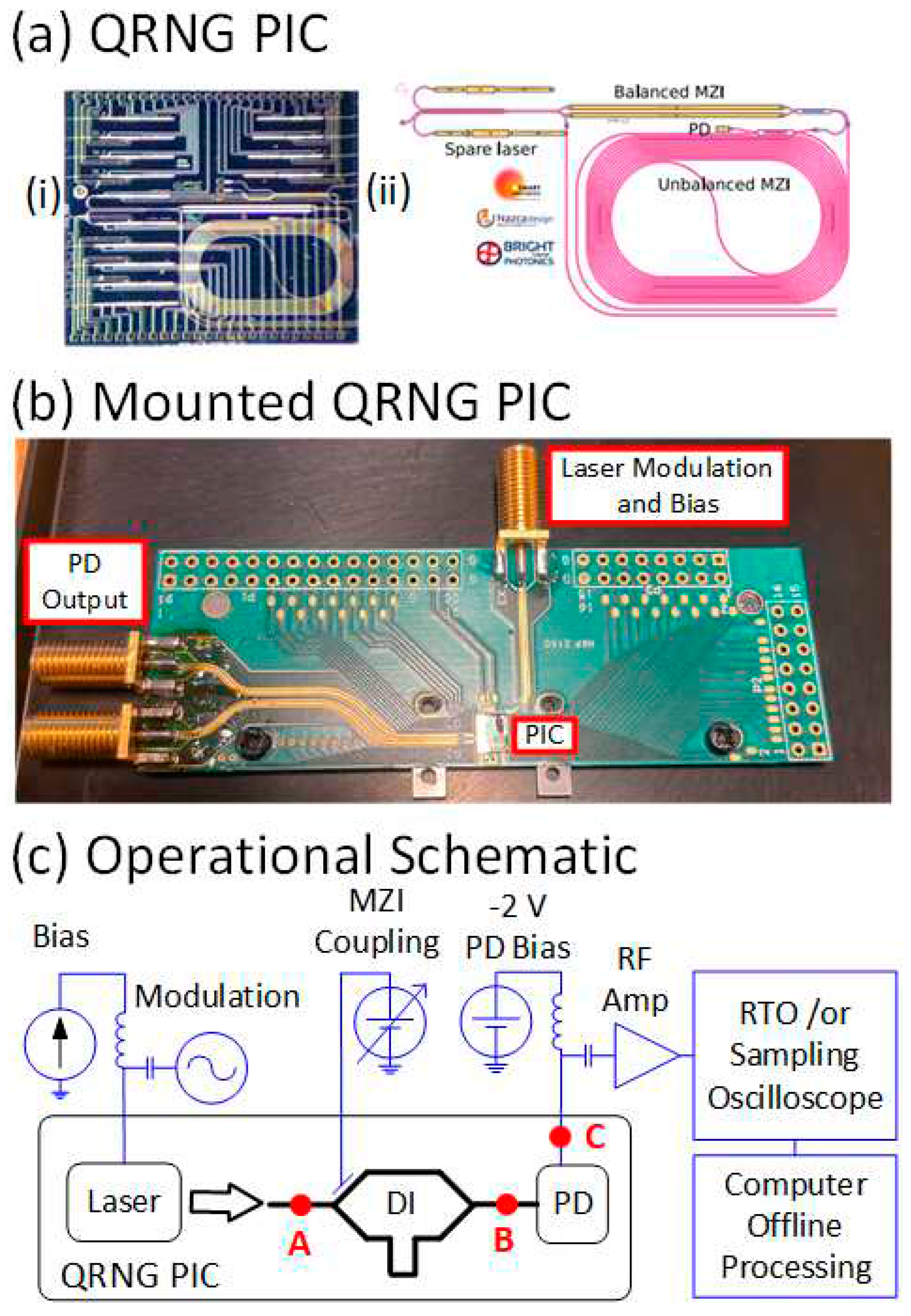
11]. A schematic of the PIC and constituent components is shown in
Figure 1. The PIC is mounted on an RF subcarrier to allow for: high-speed radio frequency (RF) connections, DC current laser bias connections, and DC voltage tuning of the DI and these are the only physical connections made with the PIC. All of the lightwave processing is performed on-chip which makes for a robust and simplified QRNG source. The system is optimized for QRNG by creating the largest distribution of random voltages at the photodetector. We find that gain-switching the laser at 1.25 GHz corresponds to the operating frequency of the delay interferometer. We present eye-diagrams of the pulsating output from the PIC for various laser bias currents as well as the corresponding distribution of the detected voltages, we find that the behavior of the voltage distribution is as expected for QRNG via gain-switching including the hallmark change in voltage distribution pattern as the bias current is increased to the point where the laser pulses are no longer seeded by SE and hence lose QRNG ability [
7]. We take one of the measured output pulsation waveforms to generate a random bit stream that we show passes the NIST statistical test suite (STS) [
12].
2. Device and Experimental Setup
Full details of the PIC have previously been published [
11], here we summarize the important features. A schematic of the PIC, mounted PIC on an RF test board, and the experimental setup is shown in
Figure 1(a),
Figure 1(b) and
Figure 1(c) respectively. The PIC is built upon an InP substrate with distributed feedback laser, Mach-Zehnder interferometer and photo-detector integrated onto the same photonic chip. The PIC is mounted on an RF testboard, shown in Figure
1(b), with ~10 GHz RF bandwidth that suffices for the purposes of this study. The laser gain—switching RF signal is a +13 dBm RF sinewave at a frequency of 1.25 GHz and electrically coupled using a bias tee with the DC laser bias current, from just above threshold to three times threshold, and applied to the coaxial connector for laser modulation and bias on the board. The electrical signals travel via RF stripline circuitry that is wirebonded to the laser. The photodiode output is wirebonded to another stripline RF waveguide and then connected to an external bias tee configured to apply a -2 V voltage to the photodiode as well as amplifying the random-amplitude pulsation signal. The pulsations are observed on a sampling oscilloscope which facilitates the optimization of the random signal. The random signal is optimized for largest voltage swing by varying the modulating frequency, drive amplitude and DI bias. In order to investigate the distribution and test for randomness the pulsation output is recorded using digital real time oscillography with four million voltage samples taken at 10 GSa/s.
In initial numerical study to get a better understanding of the process we use the same stochastic laser model as described in our previous works, the equations and parameters are given in
Appendix A. The simulated optical signal at specifically identified points along the PIC from
Figure 1(c) are presented in
Figure 2, showing laser pulsation, random amplitude pulsation after the DI, and the lowpass filtered pulsation signal.
To show the QRNG properties a random bitstream is created from the voltage waveform at a high laser bias with maximum range of random voltage and passed through the NIST STS tests.
3. Results
We now present the results of the amplified PD voltage to show the voltage distribution of the QRNG signal from the PIC. We show the measured eyediagram from the sampling oscilloscope first because this shows exactly where the QRNG signal exists in the received signal. We then show the PD voltage distribution of the detected QRNG signal along with PD voltage distributions from a numerical laser simulator. Finally we report on the results of the generated QRNG bit pattern through the NIST STS program [
12].
3.1. Sampling oscilloscope eyedigrams
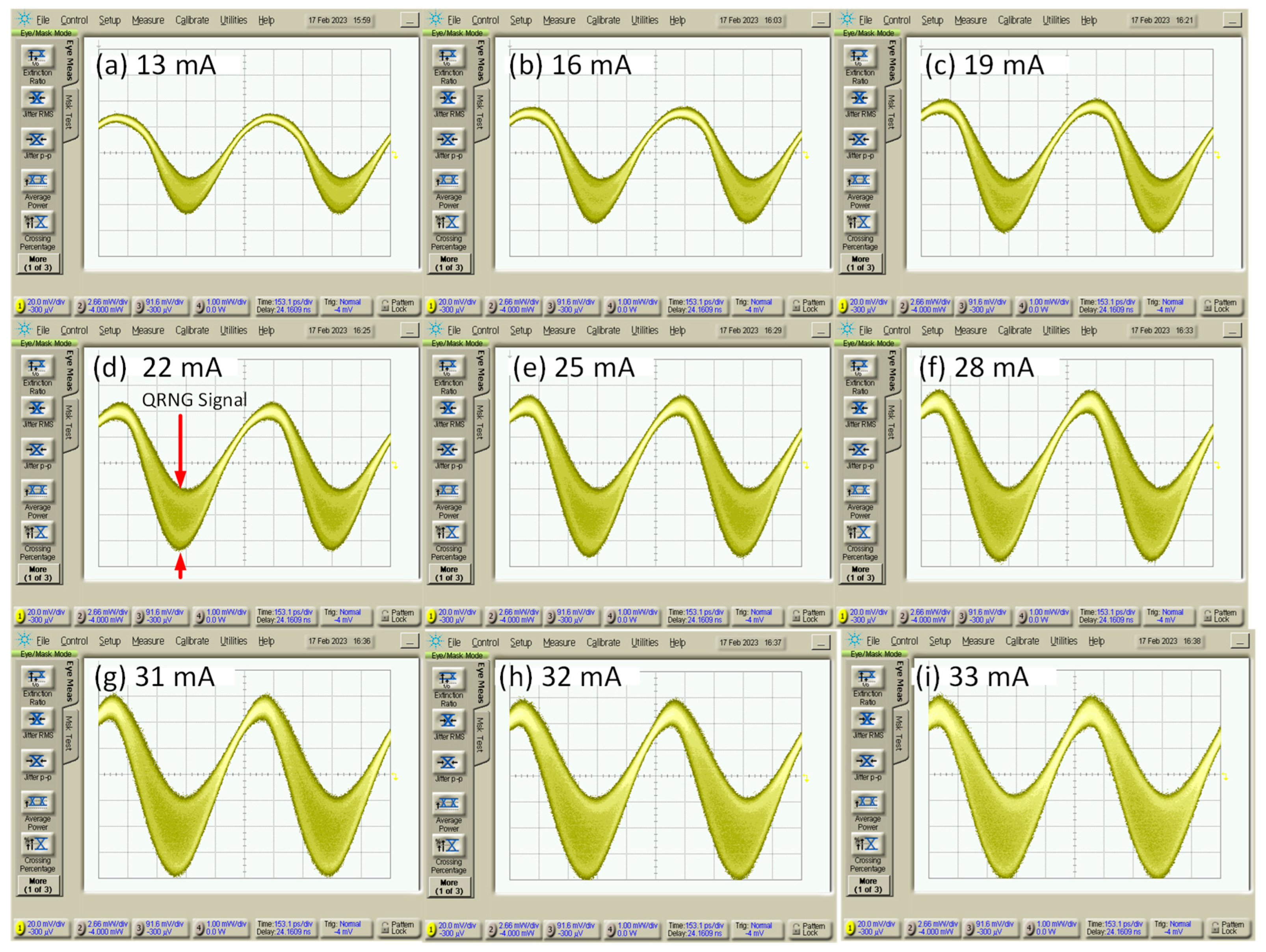
A sampling oscilloscope of 30 GHz electrical bandwidth is synchronized by tapping off 10% of the RF power from the RF driving signal to trigger the sampling oscilloscope. The amplified PD output is then captured by the sampling oscilloscope (note that the voltage is inverted after the amplifier). In the eyediagram mask mode, the oscilloscope overlays detected voltage waveforms over two modulation periods. Each eyediagram plot is the accumulation of voltage values detected over at least two minutes duration. The eyediagrams for nine different laser bias currents are shown in
Figure 3. For each scenario, there exists one signal sampling instance per modulation cycle that yields a large random voltage distribution, as indicated in
Figure 3(d). As is clear from the trend in all of
Figure 3, the voltage distribution range increases with increasing laser bias current which is as expected for QRNG signals from delayed interference gain-switched laser topology [
7]. There is however a maximum bias for which a random amplitude pulsation exists because at larger biases the RF drive signal may not be strong enough to drive the laser below threshold and hence fail to quench each pulse before the generation of the following pulse; we see this in our results for 34 mA and beyond.
3.2. QRNG voltage distribution
To measure the voltage distribution we swap the sampling oscilloscope for real time oscillography (RTO), because the sampling technique of the sampling oscilloscope only takes samples at different relative timings of the signal over many periodic cycles of the signal, hence the sampling oscilloscope traces can only indicate the possible range of values of the QRNG signal. The RTO bandwidth and sampling rate are 2.5 GHz and 10 GSa/s respectively. Since the frequency of the modulating signal is 1.25 GHz and the sampling rate is 10 GHz, we therefore capture eight samples per modulation period. A total of four million samples were captured which was the limit of the RTO employed, yielding a total of 500,000 QRNG voltage samples per detected RTO waveform.
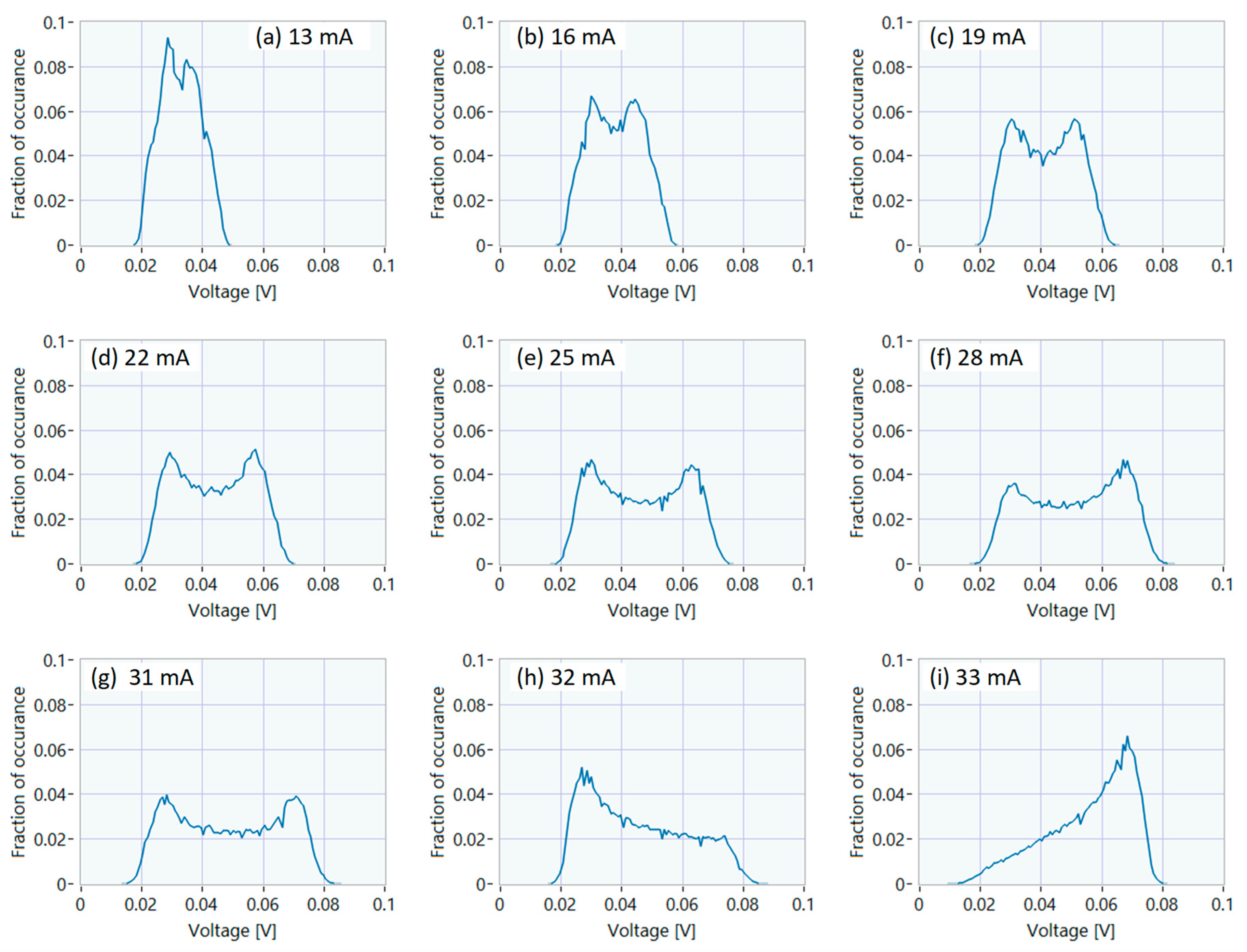
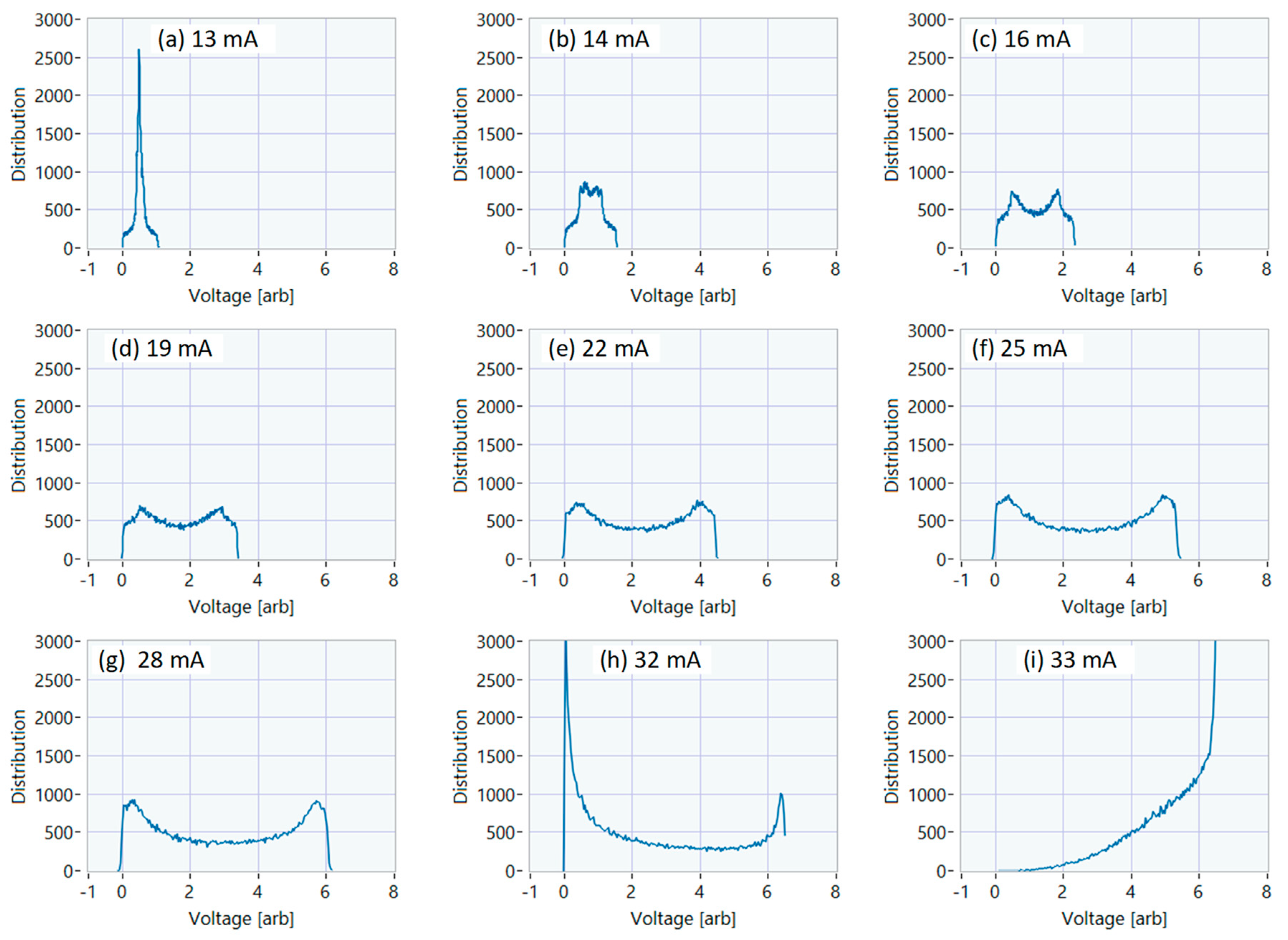
In our scenario, the QRNG signal is the minimum detected voltage within a block of 16 samples from the upsampled RTO waveform, and the QRNG signal is built up by selecting the minimum voltage over every modulation period, which is 16 samples in our case. The voltage distributions with increasing laser bias current are shown in
Figure 4. Note the presence of all of the hallmarks of the QRNG obtained by laser gain-switching and compared with the general trend established in [
7] (i) the increase in the range of voltage as the bias current is increased, (ii) the sharp cutoff in voltage outside the range of detected voltages, (iii) characteristic peaks at both ends of the voltage range arising from phase to amplitude conversion from the DI, and (iv) the change in the distribution from being centered around the lower voltage peak to being centered around the higher voltage peak as the bias current increases from 32 mA to 33 mA in
Figure 4(h) and
Figure 4 (i). Note that at sufficiently high bias currents (34 mA and higher) the RF signal can no longer gain-switch the laser below laser threshold and there is no wide range voltage distribution.
3.3. Results of the NIST STS tests
We concentrate on analyzing the QRNG signal for the case of laser bias at 22 mA (
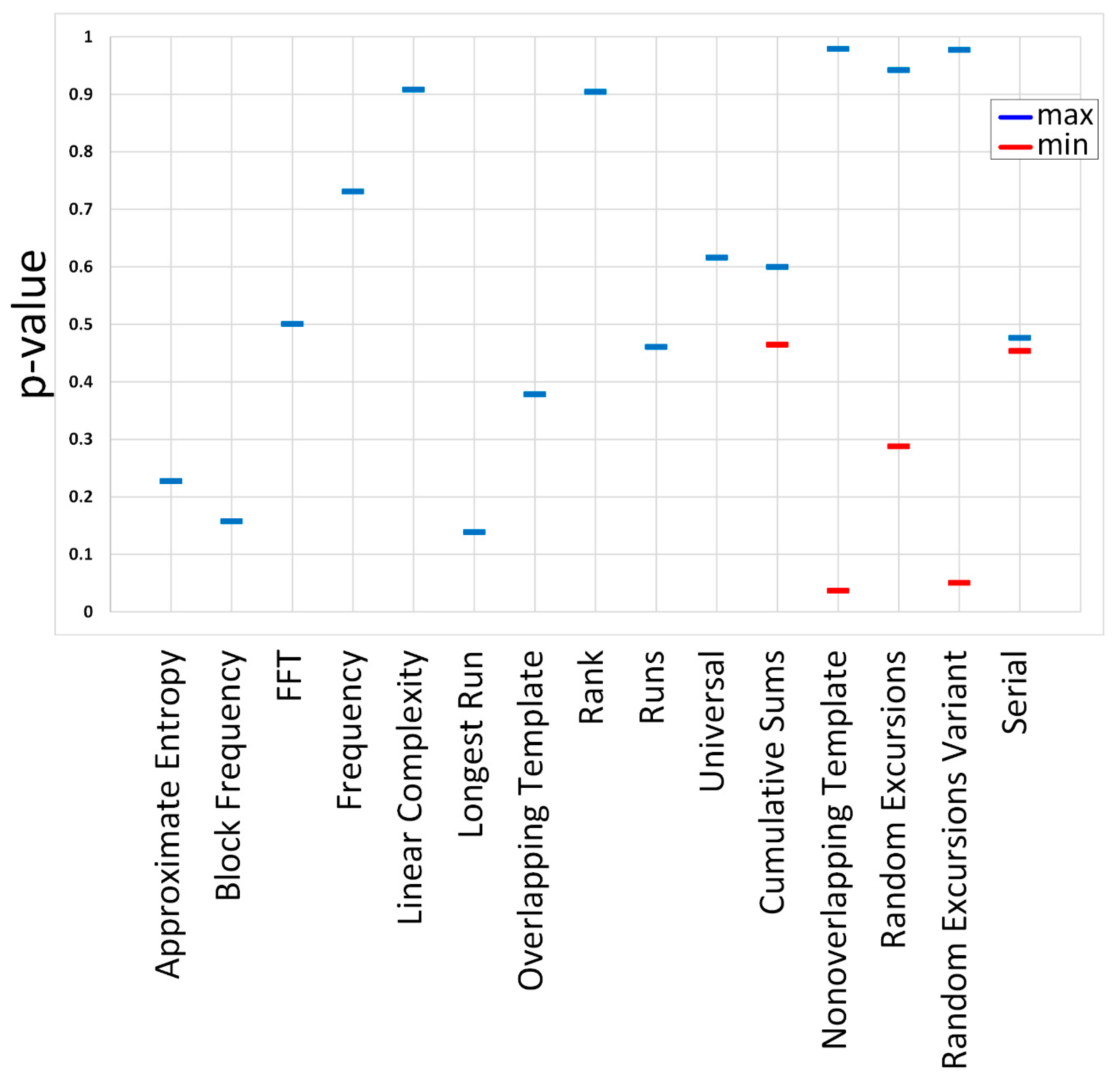
Figure 4(d)), because this is mid-range between the laser threshold current (~11 mA) and maximum laser bias allowing for QRNG signal generation (33 mA). To remove quantization effects from the low voltage amplitude signal from the RTO, the RTO waveform is upsampled by a factor of two and interpolated now giving 16 samples per modulation period. We take the upsampled RTO trace and convert to random bits by applying a binary decision threshold at 0.0464 V and creating a copy of the QRNG bit stream, applying a circular shift of 100,000 samples to the copy and then applying an exclusive-OR operation with the original QRNG bit stream. The NIST STS tests are applied to the output bit stream. We found that the QRNG bit stream passed all of the tests with the p-values arising from each test shown in
Figure 5. The comprehensive results of the STS tests are given in the supplementary material, and we disclose the following for independent verification: complete results files of the NIST STS tests; the upsampled RTO trace; the bit stream generated after binary thresholding; and the delayed and XOR bit stream that is then used as input to the STS tests.
3.4. Simulation results of the QRNG signal
For completeness we present simulated PD voltage distributions arising from the laser gain-switching with delay interferometer. We take the complex-valued laser field model that we have used extensively to simulate laser gain-switched systems [
10,
13,
14]. The details are in the Appendix. The laser field equations are much preferred to use in this scenario rather than having separate rate equations for photon density and laser phase because of the difficulty in correctly adding random photons when the laser photon density goes to zero i.e. employing random numbers from a Gaussian distribution can drive the photon density negative yielding non-physical results. We acknowledge the lack of the small correlation between the random carrier density and laser photon density when considering the complex-field approach; the results we present show that the complex-valued field rate equation suffices to capture the main peculiarities of the gain-switched QRNG system.
The total system simulator comprises a laser simulator considering lumped rate equations that consider stochastic sources for the carrier density and spontaneous emission. A delay interferometer that shifts and adds a quadrature rotated (multiply the complex field by ‘
j’) laser field,
E, shifted by precisely one modulation period; the laser modulation frequency should be adjusted to produce an integer number of laser samples over one modulation period i.e. the numerical sampling frequency should be an integer multiple of the RF modulation signal. The PD voltage is proportional to |
E|
2 followed by a tenth order Butterworth lowpass filter with bandwidth twice that of the modulating signal. The optimum sampling instance is obtained by taking 100 arrays with each array having a duration of one full modulation period, the index at which the maximum voltage is found for each array, the most frequent index obtained from the 100 arrays becomes the offset at which the RNG sample is taken from each modulation period. We simulate over 100,000 modulation periods thus collecting 100,000 RNG samples from the simulator. Histograms of the simulated RNG voltages are obtained and plotted in
Figure 6.
The simulations were performed at various laser bias current levels as per the experiments; we find that the simulation yields similar voltage distributions as per the experiments including the peculiarities of (i) increased voltage distribution with respect to bias, (ii) peaks at each side of the distribution, (iii) sharp falloff in the voltage at the lowest and largest voltages, (iv) the swing to lower and higher edge of the distribution as the bias current is increased such that the laser is no longer being gain-switched. There is good qualitative agreement between the simulations and the experiments.
4. Discussion
We have shown conclusively that a PIC containing a gain-switched laser and delay interferometer with only electrical and RF bondwire connections can produce a QRNG signal. We verify that voltage distributions are as expected with similar QRNG systems with discrete lasers and delay interferometers. The results are confirmed by performing a numerical simulation of the entire laser and delay interferometer system.
One aspect of the experiment that we did not highlight is that the PIC itself was operated without any thermoelectric control, this in itself prompts an investigation into the long term stability of this system to produce a QRNG signal without expensive thermoelectric control this should be feasible because of the low RF drive power needed to create the laser pulsations, and hence be able to produce a robust QRNG system in a small form factor package.
5. Patents
Francisco J. Díaz Otero, David Álvarez Outerelo, “Generador cuántico de números aleatorios”, Spain, no. PCT/ES2021/070179, October 07, 2021.
Author Contributions
Conceptualization, L.B., D.O., F.O.; methodology, S.D., L.B., D.O., F.O.; software, S.D.; validation, S.D., L.R., D.O., F.O., L.B.; formal analysis, S.D, L.R.; investigation, S.D. , A.S. , L.B.; resources, L.B., D.O., F.O. , F.S; data curation, S.D.; writing—original draft preparation, S.D., L.B.; writing—review and editing, S.D., L.R., D.O, F.O., A.S., F.S., L.B.; visualization, S.D., A.S. D.O.; supervision, L.B., D.O., F.O.; project administration, L.B.; funding acquisition, L.B., D.O., F.O.
Funding
Funding for this work was provided for by Science Foundation Ireland through project 12/RC/2276_P., EU Horizon 2020 through the following projects: MSCA Agreement No. 847652, and MSCA H2020-ITN-2018-EDIFY (Contract number 813467).
Data Availability Statement
We make available the RTO waveform, NIST STS test results folder and QRNG bit sequences for independent verification.
Acknowledgments
The Galician Regional Government (consolidation of Research Units: AtlantTIC).
Conflicts of Interest
The authors declare no conflict of interest.
Appendix A
We provide details of the simulated QRNG system. The main model is that of the stochastic model for semiconductor lasers. We have used this model in many previous works to study optical frequency comb generation and for laser injection locking phenomena [
10,
13,
14]. The complex-valued envelope of the laser optical field is used to avoid numerical instability issues when the squared magnitude of the laser field (photon density) goes to zero under gain-switching such that the stochastic spontaneous emission terms do not erroneously make the photon density have a negative value.
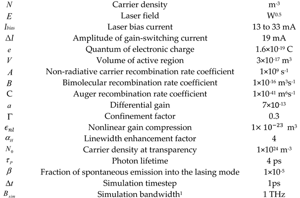
Where all of the symbols have their usual meaning and are
defined in
Table I. The carrier density is given by and is the envelope of
the laser optical field and related to the photon density in the laser. The
first term on the right hand side of (1) represents the laser bias and
sinusoidal modulating current. Carrier recombination is given by for nonradiative,
bimolecular and Auger recombination respectively; the third term represents
stimulated emission. is a complex-valued
quantity describing the envelope of the optical field and encompasses all
amplitude and phase modulation effects imposed by gain-switching; is normalized such
that represents the
photon density of the laser field.
denotes stochastic carrier recombination (which will be
defined later). The first term on the right-hand side of (1) describes the
complex gain of the laser field. The gain coefficient is given by , where a is
the differential gain and is
the carrier density at transparency. is
the cavity lifetime. The final term is the random addition of
spontaneous emission due to bimolecular recombination into the lasing field,
denoting spontaneous emission into the lasing field.
The stochastic terms are appropriately scaled for
numerical computation (1) and (2) with , where is the step time. We
solve the system of equations using Huen’s predictor-corrector method.
Each term
are independent identically distributed random samples taken from a Gaussian
random number generator with unity variance. The two
e terms for the
spontaneous emission correspond to the in-phase “I” and quadrature “Q”
components.
Table I.
Definition of laser parameters and their values used in the simulations.
Table I.
Definition of laser parameters and their values used in the simulations.
| Symbol |
Definition |
Value and/or unit |
 |
For convenience we take the PD current is taken to be , a digital tenth order Butterworth low pass filter with a 3 dB bandwidth of twice the gain switching modulation frequency is used to simulate bandwidth constraints in the entire system. To model the DI: we note that the numerical timestep is 1 ps; the delay of the interferometer is 800 ps which is importantly an integer number of samples of the complex numerical array. The 800ps DI is modeled by shifting the samples by 800 samples, multiplying by ‘j’ and adding the two arrays, . An optimum sampling instance is found and then a histogram of the distribution of the DI output voltage is made.
References
- Ma, X.; Yuan, X.; Cao, Z.; Qi, B. and Zhang, Z.,”Quantum random number generation. npj Quantum Inf 2, 2016, 16021.
- See for example: Quantum random number generation applications. Available online: https://www.idquantique.com/random-number-generation/applications/ (accessed on July 2023).
- Ito, H.; Yokoyama, H.; Murata, S. and Inaba H , "Picosecond optical pulse generation from an r.f. modulated AlGaAs d.h. diode laser", Electron. Lett., 1979, 15, 738–740. [Google Scholar] [CrossRef]
- Osinski, M. and Adams, M , "Picosecond pulse analysis of gain-switched 1.55 µm InGaAsP laser,". IEEE J. of Quantum Electron. 1985, 21, 1929–1936. [Google Scholar] [CrossRef]
- Gunning, P.; Lucek, J.K.; Moodie, D.G.; Smith, K.; Davey, R.P.; Chernikov, S.V.; Guy, M.J.; Taylor, J.R. and Siddiqui AS. “Gainswitched DFB laser diode pulse source using continuous wave light injection for jitter suppression and an electroabsorption modulator for pedestal suppression,”. Electron. Lett. 1996, 32, 1010–1011. [Google Scholar] [CrossRef]
- Anandarajah, P. M.; Maher, R.; Xu, Y. Q.; Latkowski, S.; O'Carroll, J.; Murdoch, S. G.; Phelan, R.; O'Gorman, J. and; Barry, L. P. “Generation of Coherent Multicarrier Signals by Gain Switching of Discrete Mode Lasers,” IEEE Photon. J. 2011, 3, 112–122. [Google Scholar]
- Lovic, V.; Marangon, D.G.; Lucamarini, M.; Yuan, Z. ; and Shields A.J, “Characterizing Phase Noise in a Gain-Switched Laser Diode for Quantum Random-Number Generation,”. Phys. Rev. Applied 2021, 16, 054012. [Google Scholar] [CrossRef]
- Quirce, A. and Valle, A “Random polarization switching in gain-switched VCSELs for quantum random number generation,”. Opt. Expr. 2022, 30, 10513–10527. [Google Scholar] [CrossRef] [PubMed]
- Shakhovoy, R.; Sharoglazova, V.; Udaltsov, A.; Duplinskiy, A.; Kurochkin, V. and Kurochkin, Y, ” Influence of chirp, jitter, and relaxation oscillations on probabilistic properties of laser pulse interference,”. IEEE Quantum Electron. 2021, 57, 2000307. [Google Scholar] [CrossRef]
- Ó Dúill, S.P.; Zhou, R.; Anandarajah, P.M.; Barry, L.P. “Analytical approach to assess the impact of pulse-to-pulse phase coherence of optical frequency combs,” IEEE J. Quantum Electron. 2015, 51, 1200208. [Google Scholar]
- Chrysostomidis, T.; Roumpos, I.; Alvarez Outerelo, D.; Troncoso-Costas, M. ; Moskalenko,V; Garcia-Escartin, J. C.; Diaz-Otero, F. J.; and Vyrsokinos, K., “Long term experimental verification of a single chip quantum random number generator fabricated on the InP platform,”. EPJ Quantum Technol. 2023, 10, 5. [Google Scholar] [CrossRef]
- Rukhin, A.; Soto, J.; Nechvatal, J.; Smid, M.; Barker, E.; Leigh, S.; Levenson, M.; Vangel, M.; Banks, D.; Heckert, A.; Dray, J. and Vo, S, “A Statistical Test Suite for Random and Pseudorandom Number Generators for Cryptographic Applications,”. NIST Special Publication 2010, 800, 22. [Google Scholar]
- Duill, S. P. ; and Barry, L. P., “High-resolution simulation of externally injected lasers revealing a large regime of noise-induced chaos,”. MDPI Photonics 2022, 9, 83. [Google Scholar]
- Ó Dúill, S.P.; Anandarajah, P.M.; Zhou, R.; Barry, L.P. “Numerical investigation into the injection-locking phenomena of gain switched lasers for optical frequency comb generation,” Appl. Phys. Lett. 2015, 106, 211105. [Google Scholar]
|
Disclaimer/Publisher’s Note: The statements, opinions and data contained in all publications are solely those of the individual author(s) and contributor(s) and not of MDPI and/or the editor(s). MDPI and/or the editor(s) disclaim responsibility for any injury to people or property resulting from any ideas, methods, instructions or products referred to in the content. |
© 2023 by the authors. Licensee MDPI, Basel, Switzerland. This article is an open access article distributed under the terms and conditions of the Creative Commons Attribution (CC BY) license (http://creativecommons.org/licenses/by/4.0/).
