1. Introduction
This paper reports on an investigation of a new material system with the potential for monolithic integration of lasers, power amplifiers, modulators, waveguides, detectors, together with microwave electronics on a signal chip, to achieve microwave photonic systems [
1]. Given that the silicon semiconductor has been the backbone of our economic and military strength, one might think that the best platform for this photonic system is to integrate the laser light source, active optical elements, and operating microwave electronics all on a silicon chip. However, while silicon has been more than great for electronics, it has been less so for photonics [
2]. For example, despite many efforts by the photonics community over a long period of time, a satisfactory silicon laser has not yet been developed. This is due to the fact that silicon is an indirect bandgap semiconductor [
3,
4]. As a result, excited electrons in silicon are good for producing current, but not so much for producing light. In fact, millions of excited electrons in silicon may produce only a few photons [
5]. However, a similar structure using a III-V or group IV semiconductors may only require a few excited electrons to produce one photon [
5,
6].
As a result, one approach currently taken is to use an indium phosphide (InP) semiconductor laser, epitaxially grown on a separate InP substrate and bonded directly onto a silicon substrate [
7]. While this approach has been very successful, the InP substrate is expensive [
8] and a bonded InP laser [
9] does come with the potential for coupling losses and reliability issues that can cause important consequences for optical power budgets, energy efficiency, and especially cost. Consequently, delivering an efficient laser technology, monolithically integrated with optical and electrical functionality at RF-THz frequencies onto a single chip, and at low cost, has been and remains both a significant challenge and an exciting opportunity.
Addressing this challenge to microwave photonics, we have pursued the fabrication of a monolithic integrated group IV GeSn semiconductor laser [
10,
11,
12], on a sapphire substrate. Sapphire is already used as an ideal substrate for microwave devices [
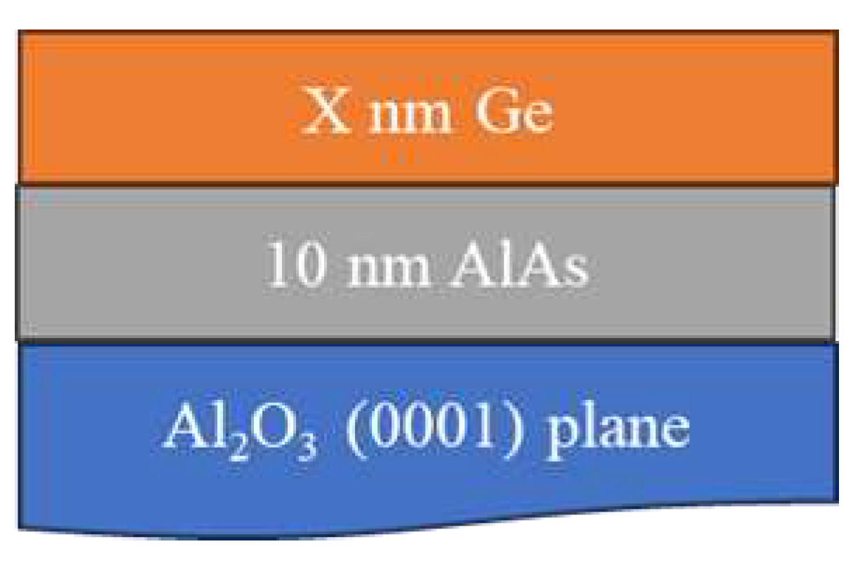
13] and adding optical elements to sapphire is an attractive possibility to realize microwave photonic chips. The potential outcome is monolithic integration of a GeSn laser and detector, together with microwave devices, all on a sapphire substrate. As a first step to investigate the potential for growth of GeSn on sapphire, we have reported on the growth of germanium on sapphire, with and without an AlAs buffer layer, as a function of growth temperature [
14]. This led to 400
oC as the best growth temperature for Ge on an AlAs/sapphire substrate. Here, we have taken our investigation one step further and probed the role of the thicknesses of the Ge thin film to obtain the needed high-quality Ge to support quality GeSn thin films. Indeed, we have found that the thickness does play a significant role on the topology and quality of the Ge film requiring about two microns of Ge.
3. Results and Discussion
X-ray diffraction (XRD) measurements were performed for the study of the crystal structure of the Ge layers after the growth. For all samples,
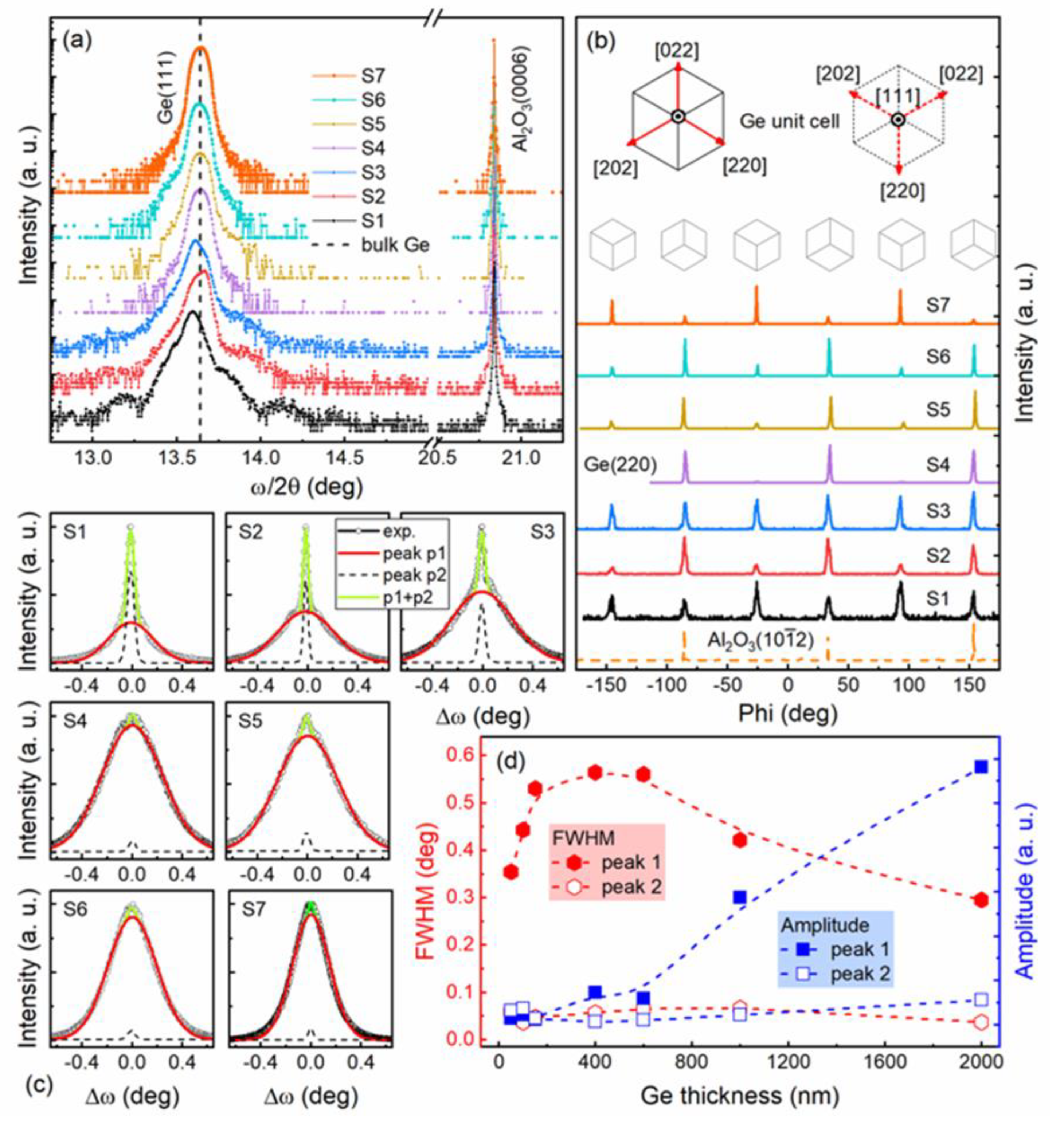
Figure 2a shows the symmetrical ω/2θ scans in which ω = θ. Hence, the direction of the scan of the diffraction vector is perpendicular to the sample surface and only the surface-symmetric planes are observed. As a result, the Ge (111) peak is seen along with the Al
2O
3(0006) peak, indicating that the out-of-plane orientation of Ge is (111). The Ge (111) peak is in proximity to the position of bulk Ge (vertical dashed line), indicating a low level of strain (~ 0.2 ± 0.1%) in the Ge structure of all samples. Common to the x-ray diffraction from all samples, the shoulder at the right side of the Ge (111) peak corresponds to the thin AlAs layer. This is confirmed by the growth of a reference sample without the AlAs 10 nm wetting layer, for which the shoulder peak was not observed on the XRD spectrum (not shown here).
The azimuthal orientation of Ge (111) and its epitaxial relationship with the Al
2O
3(0001) substrate were also studied using the XRD phi scan (φ-scan) measurements (
Figure 2b). By performing a φ-scan, an (
) plane is brought into the Bragg diffraction condition as the sample is rotated around the φ-axis (surface normal). For the {220} family of planes of Ge epitaxial films, only a set of three planes (220), (202), and (022), are expected to satisfy the Bragg diffraction condition when performing the φ-scan of 360° [
15]. Therefore, the emergence of the six Ge peaks in
Figure 1b is attributed to twin grains observed for samples S1 to S3 that are 60° rotated with respect to each other (inset in
Figure 2b) consistent with the RHEED observations during growth (not shown here). Additionally, the epitaxial relationship between the epilayer and substrate is established by the φ-scan data for the Al
2O
3(
) reflection. The alignment of the Ge(220) and Al
2O
3 peaks is consistent with two epitaxial relationships Ge(111)[110] parallel to Al
2O
3(0001)[
] and Ge(111)[110] parallel to Al
2O
3(0001)[
], both corresponding to a huge lattice mismatch of 42%. Further growths for S4 to S7 indicates a transition to favor a single twin.
The structural quality of the Ge epilayers was also investigated by comparing the linewidth of the XRD ω scan of the Ge (111) plane. The potential factors determining the linewidth are the lateral correlation length, density of dislocations, as well as tilt angles [
16,
17,
18,
19].
Figure 2c shows that the XRD peak of the 50 nm sample has the narrowest linewidth. The increase in Ge thickness is accompanied by the emergence of a complex diffraction pattern which is deconvolved into a narrow and broad peak (
Figure 2c). The full width at half maximum (FWHM) of the broader peak is shown to increase with the Ge layer thickness for S1 to S3 but decrease for S4 to S7 (
Figure 2d), while the narrow component remains the same. Consistent with representing two different effects, a plot of the amplitude of each component versus thickness shows an increase for the broad peak with increasing Ge thickness while the relative amplitude of the narrow peak remains nearly the same. As a hypothesis, we take the narrow peak to represent the early stage of growth for each sample, while the broader peak represents the growth above about 50 nm and depends on thickness.
To investigate further, characterization using Raman spectroscopy (RS) was performed to examine the strain in each sample. In contrast to the deep penetration of x-rays through the Ge samples, the penetration depth of the He-Ne laser beam used in the Raman study is only about 40 nm due to the high absorption coefficient of the Ge lattice [
14]. Therefore, the Raman results are representative of the topmost layers of the Ge samples, and in particular, the near-surface strain state of the Ge films allowing for the study of strain as a function of growth.
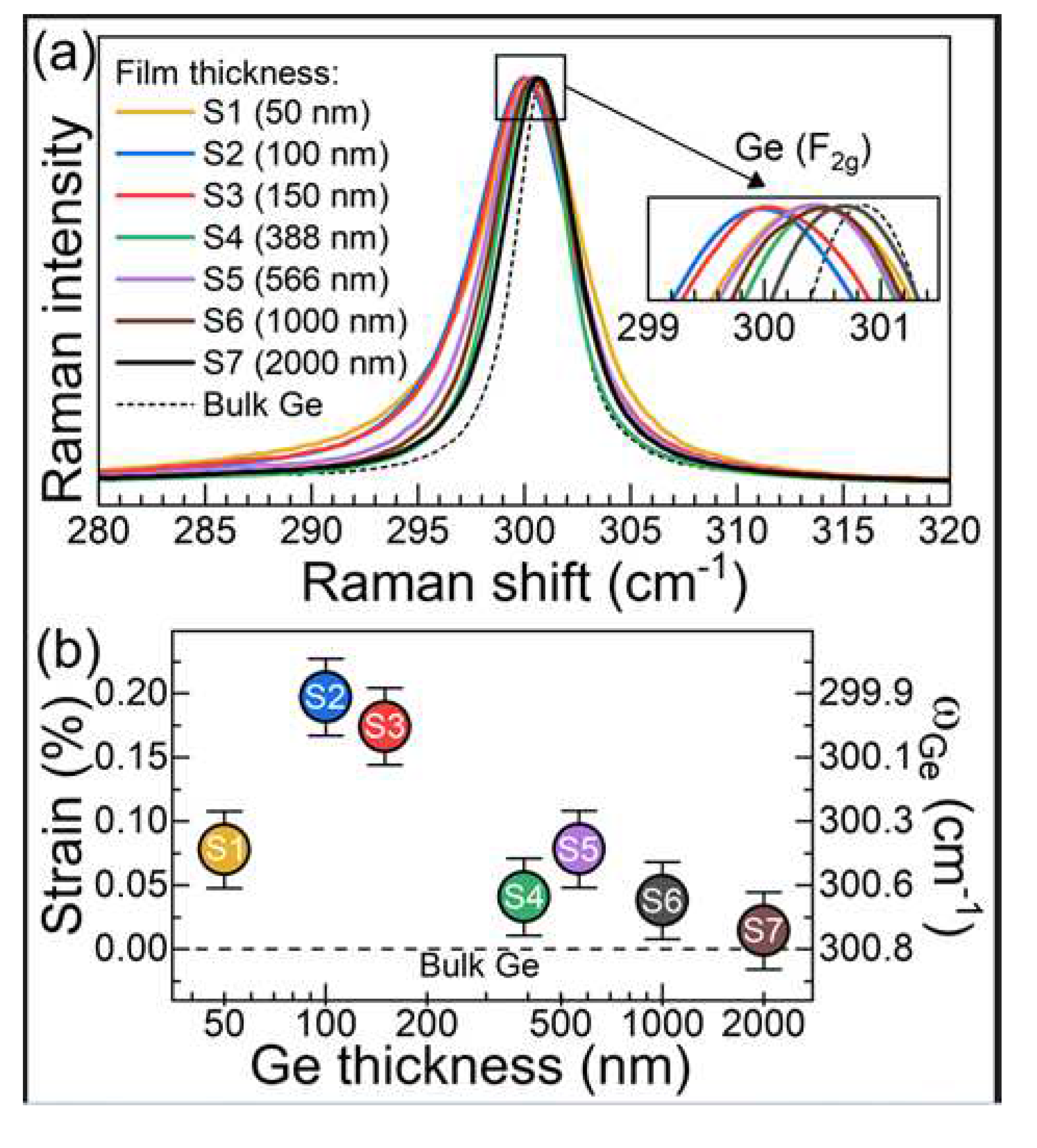
Figure 3a shows the Raman spectra of each film compared with bulk Ge. A single peak is seen at around 300 cm
-1 [
14], which corresponds to the triply degenerated mode of symmetry F
2g of the Ge cubic structure. This is the most intense first-order mode of the Ge lattice, and the lack of a commonly reported low-frequency adjacent band attributed to a disorder-activated origin confirms the absence of an amorphous Ge phase [
20] within the analyzed crystal volume. The frequency of the Ge (F
2g) mode was used to estimate the in-plane strain (
) in each sample using the deformation potential of the F
2g symmetry for the Ge lattice (
=
= 415 cm
-1) [
21]. The strain behavior as a function of film thickness (
Figure 3b) indicates relatively unstrained Ge islands for sample S1 followed up by strain build up for the Ge layer of samples S2 and S3, and strain relief starting with S4. Our data on twinning, omega linewidth, AFM, and Raman, as a function of thickness (
Figure 3a) suggest that strain builds for samples S1 to S3 at the boundaries between twinned grains. Note that the Ge grains of sample S1 are relatively freestanding. This is followed by a decrease in strain from S4 to S7 which is correlated to the transition to a single twin structure that then continues as a function of thickness resulting in improvement in material quality as evidenced by the observed behavior (
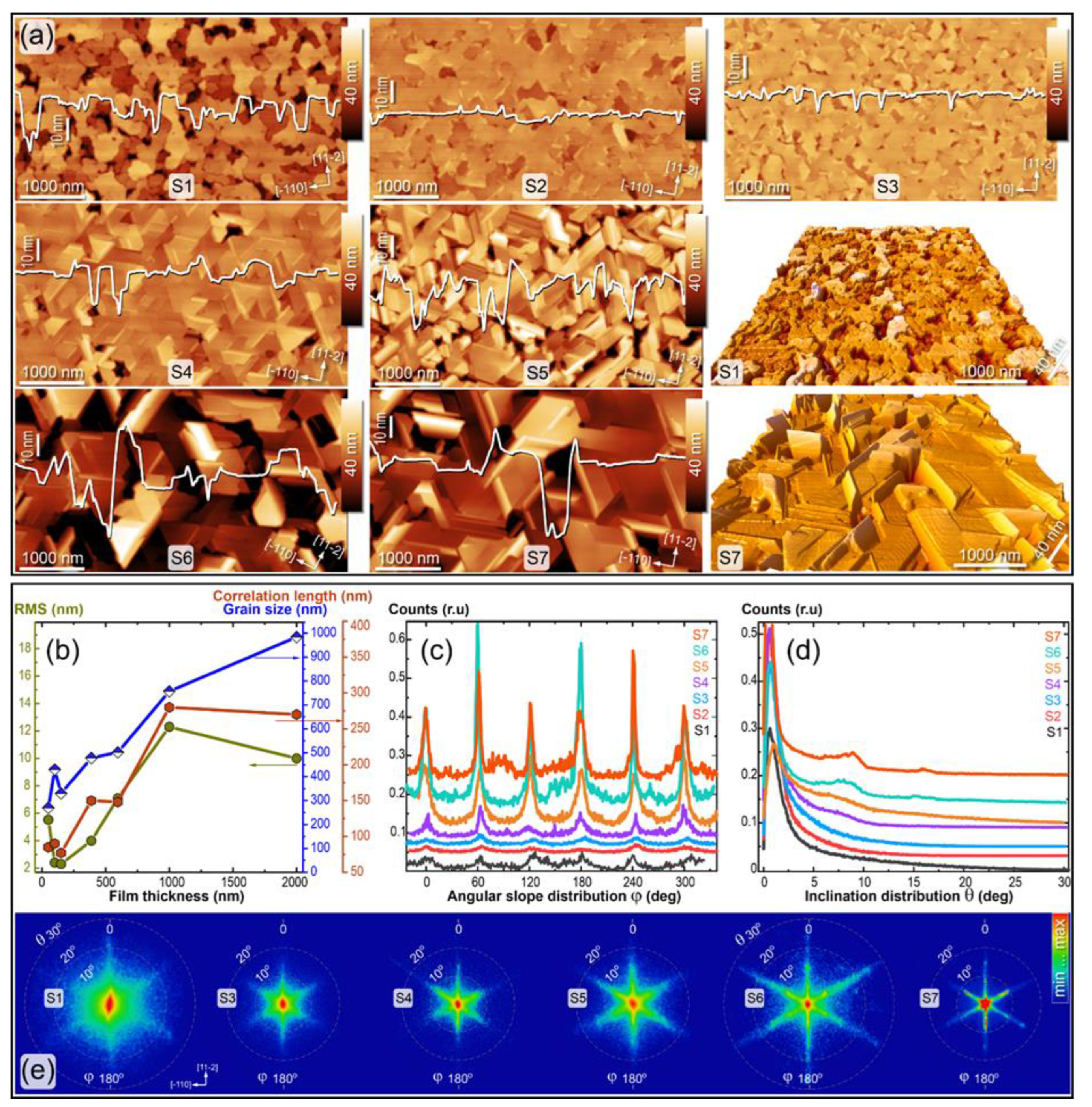
Figure 2c, d) of the linewidth of the broad component of the deconvolved peaks of the omega scan. At the same time the three-dimensional structures or grains observed using atomic force microscopy (AFM) of each surface (
Figure 4a), become more well defined in shape and direction as a function of Ge deposition and ripening.
To investigate further, the nature of the orientational anisotropy and definition of the grain boundaries are illustrated by plotting the bivariate polar histograms of the local surface slope and direction obtained using AFM.
Figure 4e indicates that a more well-defined geometry is developing with increasing Ge film thickness. The increasing space between twin domains, correlation length, domain size, surface smoothness, and decreasing strain omega linewidth, and transition to single twin, (
Figure 4), together indicate an improving quality of the Ge film with increasing film thickness. When the thickness of the germanium film reaches 400 nm (S4), pronounced faceting is observed along with a transition to only one of the twins. The roughness and grain size consistently increase from samples S4 to S6. However, for S7, there's a noticeable reduction in roughness and observation of photoluminescence (PL). The correlation length, depicted in
Figure 4b, provides information on the correlated lateral spacing of surface features. As expected, this length increases with the maturation of the three-dimensional structures [
22]. It also shows a reduction in the lateral spacing of surface features for sample S7.
A more statistical characterization of surface facets can be achieved through the analysis of angular slope and local inclination distributions, as shown in
Figure 4c, d. Measurements capturing the local in-plane slope orientation (
φ) and vertical inclination (or tilt,
θ) from the AFM image are consolidated into bivariate histograms, which depict facet in-plane orientations and inclinations (see
Figure 4e). As evident from
Figure 4c,e, even the thinnest Ge layer displays a subtle sixfold preferential in-plane orientation of grain boundaries. As the film thickness increases, the maxima of the angular slope distribution and the rays in the bivariate histograms become more defined. By the time the film reaches a thickness of 2000 nm (S7), the crystallographic orientations of the surface grain edges become distinctly delineated.
Additionally, the bivariate histograms for samples S6 and S7 reveal nodes in the rays, which indicate a favoured tilt of the facets. This is further highlighted by the broad maxima in
Figure 4d for samples S6 and S7. These histograms can be juxtaposed with the stereographic projection of Ge(111) presented in
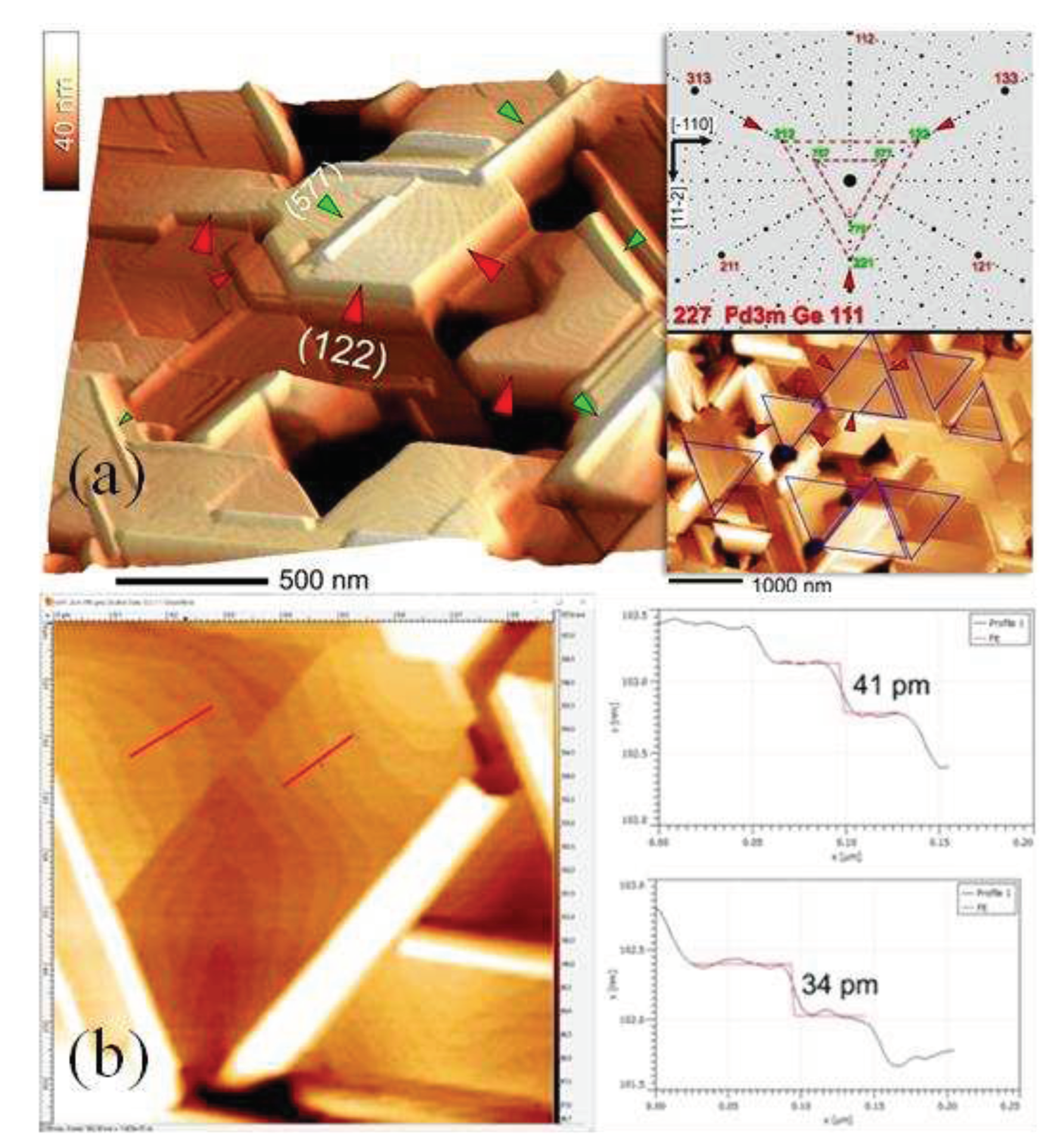
Figure 5. A facet tilt of 15.8 degrees aligns with the surface orientation (122), while a tilt of 8.5 degrees corresponds to the orientation (577). Given the symmetry of a regular triangle, added symmetry in the histograms emerges due to the simultaneous presence of step-up and step-down features in the same direction. This mirrors the existence of two opposing orientations of regular triangles, as depicted in
Figure 5a (bottom right). It's worth noting that the facets characterized by orientation (577) correlate with road-like surface relief patterns, which might be linked to certain stacking faults [
23].
The RS measurements indicated a relaxation of residual strains in samples S4 through S7. This strain relaxation manifests in the surface relief, signifying a shift from the 3D Volmer-Weber growth mechanism to a hybrid growth mode combining both 3D and two-dimensional step-flow growth. Distinct growth terraces are observable on the faceted grains, as depicted in
Figure 5b. These monatomic terraces have heights ranging from 30 to 40 pm, aligning with the interplanar spacing of 32.7 pm in germanium along the <111> direction.
As a result, we observe a correlation between strain, quality, twinning, and the interface between domains that suggest the interface between twin domains result in strain, broad omega linewidth, and the absence of PL. With further growth, stain relaxation occurs as the grains become well-defined and separated, the omega linewidth decreases, and we observe PL. For example, the 50 nm thick Ge film (S1), exhibits an RMS roughness of 5.5 nm.
Table 1 summarizes the pattern for the seven different Ge film thicknesses.
Author Contributions
Conceptualization, E.W., S.-Q.Y. and G.S; methodology, E.W., H.S. and F.M.O.; software, E.W. and H.S.; validation, E.W., H.S., O.O. and G.S.; formal analysis, E.W., P.M.L., F.M.O., H.S, Y. I.M.; investigation, E.W., C.G., M.Z.A., S.D., N.E., C.L. and S.S.; resources, E.W., M.Z.A., C.G., and S.S; data curation, E.W., P.M.L., H.S., F.M.O., and C.G.; writing—original draft preparation, E.W., H.S., F.M.O. and C.G.; writing—review and editing, E.W., H.S., F.M.O., P.M.L., C.G., S.S., S.D., N.E., C.L., M.Z.A., Y.I.M., S.-Q.Y. and G.S.; visualization, E.W. and H.S.; supervision, S.-Q.Y. and G.S; project administration, S.-Q.Y. and G.S; funding acquisition, S.-Q.Y. and G.S.; All authors have read and agreed to the published version of the manuscript.
