Preprint
Article

Wet-deposited TADF based OLED Active Layers: New Approaches Towards Further Optimization

Altmetrics

Downloads

99

Views

58

Comments

0

A peer-reviewed article of this preprint also exists.

Submitted:

28 September 2023

Posted:

30 September 2023

You are already at the latest version

Alerts
Abstract
The effects of the solvent used for the active layer materials of an OLED based on TADF emitters plays a fundamental role in solution-deposited devices. This work focuses the effects on the performance of different solvents employed to fabricate a very simple two organic layer OLED based on a green TADF emitter, under the concept of host:guest matrix. From the different results of the main figures of merit, it was possible to conclude that the OLED that used toluene as solvent for the active layer reached a maximum EQE of 14%, almost the maximum already obtained for this emitter in more complex device structures. With the analysis of the charge transport processes, it was possible to establish an explanatory model for the obtained results. Through impedance spectroscopy, additional characterization about the nature of charge transport processes was carried out. With these results, it was possible to corelate the relaxation times, with the electrical properties of the active layer, and infer about the interaction between the electrical charges and the defect levels opening new possibilities to further development in the printed OLEDs.
Keywords: 
Subject: Chemistry and Materials Science  -   Nanotechnology

1. Introduction

Organic light-emitting diodes (OLEDs) play an important role in display technology nowadays. Since Tang and VanSlyke pioneer work [1] in a thermal evaporated double organic layer device, composed by tris(8-hydroxyquinolinate)aluminum(III) (electron transport and emissive layer – ETL and EML, respectively) and an aromatic diamine (hole transport layer – HTL), a fast growth on the academical and industrial research has been remarked due to the possibility of obtaining a high efficiency OLED. [2] OLED research can be divided into five main technologies: 1st – fluorescent emitters [3]; 2nd – phosphorescent emitters [4]; 3rd – thermally activated delayed fluorescent (TADF) emitters [5,6,7]; 4th – hyperfluorescent emitters [8]; and most recently 5th – usage of non-resonant energy transfer process to pump-up OLEDs efficiency [9, 10]. Also, solution-processable protocols (i.e. spin-coating [11], blade coating [12], inkjet [13], screen printing [12], and slot-die coating [14]) have been adopted in order to achieve easy up-scaling devices, coupled with cost, energy, and material saving urgent demands. [15]
In particular, TADF dyes have been played an important role in high-efficient OLEDs’ emissive layers (EMLs) due to their capability to easy optoelectronic features tunability via simple chemical structure modifications [16, 17], which enables achievement of external quantum efficiencies (EQEs) up to the theoretical limit for a simple architecture device, coupled with wide gamma of emitting colors at entire visible electromagnetic spectrum. [18,19,20,21,22] As usual, TADF molecules are composed by an electron donor (D) and acceptor (A) moieties chemically bonded, which is capable to create a charge-transfer (CT) state, and with an orthogonal orientation between D and A parts can create a small energy barrier between first excited singlet and triplet states (ΔEST ≈ 0) [23]. When these organic dyes have those characteristics, they can undergo to a thermally activated a reverse inter system crossing (rISC), enabling TADF OLEDs to theoretically achieve internal quantum efficiencies (IQE) of 100 %, according to the singlet/triplet spin statistics [23, 24]. However, TADF molecules present strong triplet-triplet annihilation (TTA) pathways and sensitivity to the local chemical environment (solvatochromism) due to its active triplet states involved into the delayed fluorescence electronic structure reorganization. [25,26,27,28,29] Those characteristics make that the use of TADF molecules for OLED’s EML needs to apply it in a host:guest system at small concentrations, diminishing emitting loses via non-radiative recombination process. In global, a compromise between an efficient TADF process and the final device color must be considered for their emitting diodes [30, 31].
In recent years, Pereira and his co-workers [32,33,34,35] have done comprehensive studies about how to optimize electrical and morphological properties of solution-processable mixed-host layers for efficient TADF OLEDs based-on simple architectures. These mixed-host layers are composed of the poly(9-vinylcabazole) (PVK) (a well-known transparent p-type polymer) and an ambipolar, p-type or n-type semiconductive small-molecule for obtaining a balance of charge-carrier and density of injected electrons and holes into the EML. The electrical and morphological optimization of such kind of layers enables to achieve high-efficient solution-processable TADF OLEDs (EQEs beyond 15 %) [33, 34]. In special, PVK:OXD-7 (1,3-bis[2-(4-tert-butylphenyl)-1,3,4-oxadiazo-5-yl]benzene) mixed-host with 2PXZ-OXD (2,5-bis(4-(10H-phenoxazin-10-yl)phenyl)-1,3,4-oxadiazole) green-emitter TADF guest enabled Pereira’s group to achieve EQE up to 10 % in a unique organic layer OLED, best result for this material in such type of simple architecture. [32] Nonetheless, a comprehensive study about how different solvents with specifical physical-chemical properties and interactions must be done to better understanding of the local chemical environment on the OLED’s morphological, electrical, and optical features.
In this sense, herein we exploit a detailed study about how four different solvents for processing OLED’s EML, composed by PVK, 1,3-Bis(N-carbazolyl)benzene (mCP) (ambipolar semiconducting small molecule) and 2PXZ-OXD, changes their optoelectronic properties in solution-processed OLEDs by spin-coating technique. Toluene (Tol), chlorobenzene (CB), chloroform (CHCl3) and tetrahydrofuran (THF) were selected considering differences of their physical-chemical properties (vapor pressure, boiling point, viscosity, density, dielectric constant, among others) and specific chemical interactions with the EML solutes to understand its impact on the electrical and optical properties of OLEDs. Electroluminescent devices were assembled following the straightforward architecture: ITO|PEDOT:PSS|EML|TPBi|LiF|Al. Electroluminescence (EL) spectra reveal a considerable red-shit in the emission bands, according to the solvent polarity, vapor pressure and boiling point, as well as specific molecular interactions: high polarity, vapor pressure and boiling solvents (i.e., THF and CHCl3) present EL maxima band close to 525 nm, while CB and Tol solvents have EL close to 495 nm; effect probably linked to the fast evaporation of THF and CHCl3 solvents in contrast to the another ones during the thermal annealing of the active layer; also, THF solvent could have strong chemical interactions with the EML molecules, which combined with its high vapor pressure, can create more crystalline domains, accountable to form molecular aggregates that own low-energetic emissive states. Those different solvents also impact directly on the OLED’s figures of merit (FOM, particularly, Luminance L, external quantum efficiency EQE, power efficiency ηp and current efficiency ηc), achieving best results for Tol: Von = 4.0 V @ Lmax = 3270 cd m-2 @ EQEmax = 14 % ηc = 24.3 cd A-1 @ ηp = 16.9 lm W-1; small efficiency losses (roll-off) until 1000 cd m-2 for all solvents (32 %, 6 %, 1 % and 25 % for Tol, CB, CHCl3 and THF, respectively). In order to better understand those features, DC and AC electrical measurements in ambipolar, as well as only-hole and -electron devices were employed considering space-charge limited current models (SCLC) and impedance spectroscopy, respectively. Finally, this present manuscript reveals that different chosen solvent has a strong impact on the 2PXZ-OXD TADF solution-processed OLEDs, even after thermal treatment of the active-layer, regarding efficiency losses and EL emission energies, opening doors for a wide range of fundamental chemical interactions (i.e., Raman, NMR, FTIR, photophysical, and time-resolved spectroscopies), structural (small-angle and grazing incidence X-ray scattering – SAXS and GIWAXS, respectively) and morphological studies on mixed-host for high-efficient solution-processable TADF OLED.

2. Materials and Methods

2.1. Materials

Poly(ethylenedioxythiophene):poly(4-styrenesulfonate) (PEDOT:PSS) and patterned ITO-glass substrates were purchased from Ossila company. 2,2',2"-(1,3,5-Benzinetriyl)-tris(1-phenyl-1-H-benzimidazole) (TPBi) and 2,5-bis(4-(10H-phenoxazin-10-yl)phenyl)-1,3,4-oxadiazole (2PXZ-OXD) were purchased from Lumtech Ltd. Poly(9-vinylcarbazole) (PVK; MW = 1,100,000 g mol-1), 1,3-Bis(N-carbazolyl)benzene (mCP), lithium fluoride (LiF; 99.999%), Hellmanex®, toluene, chlorobenzene, chloroform and tetrahydrofuran (anhydrous and inhibitor-free grade solvents) were purchased from Sigma-Aldrich, Portugal. All chemicals were used without further purification. Figure 1 shows the simple molecular scheme of the materials employed in this work.

2.2. Photophysical Measurements

Electronic absorption spectroscopy were acquired in a Shimadzu UV-Vis UV-2100. Photoluminesce (PL) and PL excitation (PLE) spectroscopies measurements were obtained from a in a Fluorolog-3 Horiba Scientific set-up fluorimeter, using excitation and emission wavelenghts at 290 nm and 500 nm, respectively.

2.3. OLEDs fabrication and single carrier devices

ITO-glass substrates were cleaned under sonication and heat, using 2 % Hellmanex® solution for 30 minutes. Substrates were washed subsequently with hot water, acetone, and IPA for 15 minutes for each step in a heated ultrasonic bath. Then, substrates were treated with NaOH 10 %vol under sonication for 5 minutes, rigorously washed with deionized hot water, and dried with N2(g) jet. PEDOT:PSS (30 nm) were dynamically deposited by spin-coating technique (5000 rpm; 30 s), and films were annealed in a controlled oven at 120 ℃ for 10 minutes. Then, PEDOT:PSS deposited films were transferred to a N2(g) controlled atmosphere MBraun Glovebox ([O2] < 10 ppm; [H2O] < 0.1 ppm), where the solutions of 2PXZ-OXD (10 %wt) into PVK:mCP (3:2; 10 mg mL-1; ~ 50 nm) of each solvent were spin-casted as EML. Finally, TPBi (40 nm; ETL), LiF (0.5 nm; EIL) and Al (80 nm) electrical contact were thermally evaporated under ultra-vacuum conditions (p < 5x10⁻⁶ mbar), obtaining OLEDs with the following configuration: ITO|PEDOT:PSS|PVK:mCP:2PXZ-OXD|TPBi|LiF|Al. It should be noted that the ITO|PEDOT:PSS “layer” is considered an optimized anode (work function near 5.2 eV as widely reported in literature [35] – and due to the “metal-like” behavior of PEDOT:PSS we will not take it into account for the total “pure” organic layers) and, in opposite, the LiF|Al “layer” is an optimized cathode (accepted work function near 3 eV [35]), mainly due to the well-known quantum tunnelling effect thought dielectric LiF material. In such framework, we will consider (as usual) that our devices are made with only two “pure” organic layers (in electrical point of view). The final active area of each OLED was 4.5 mm2.
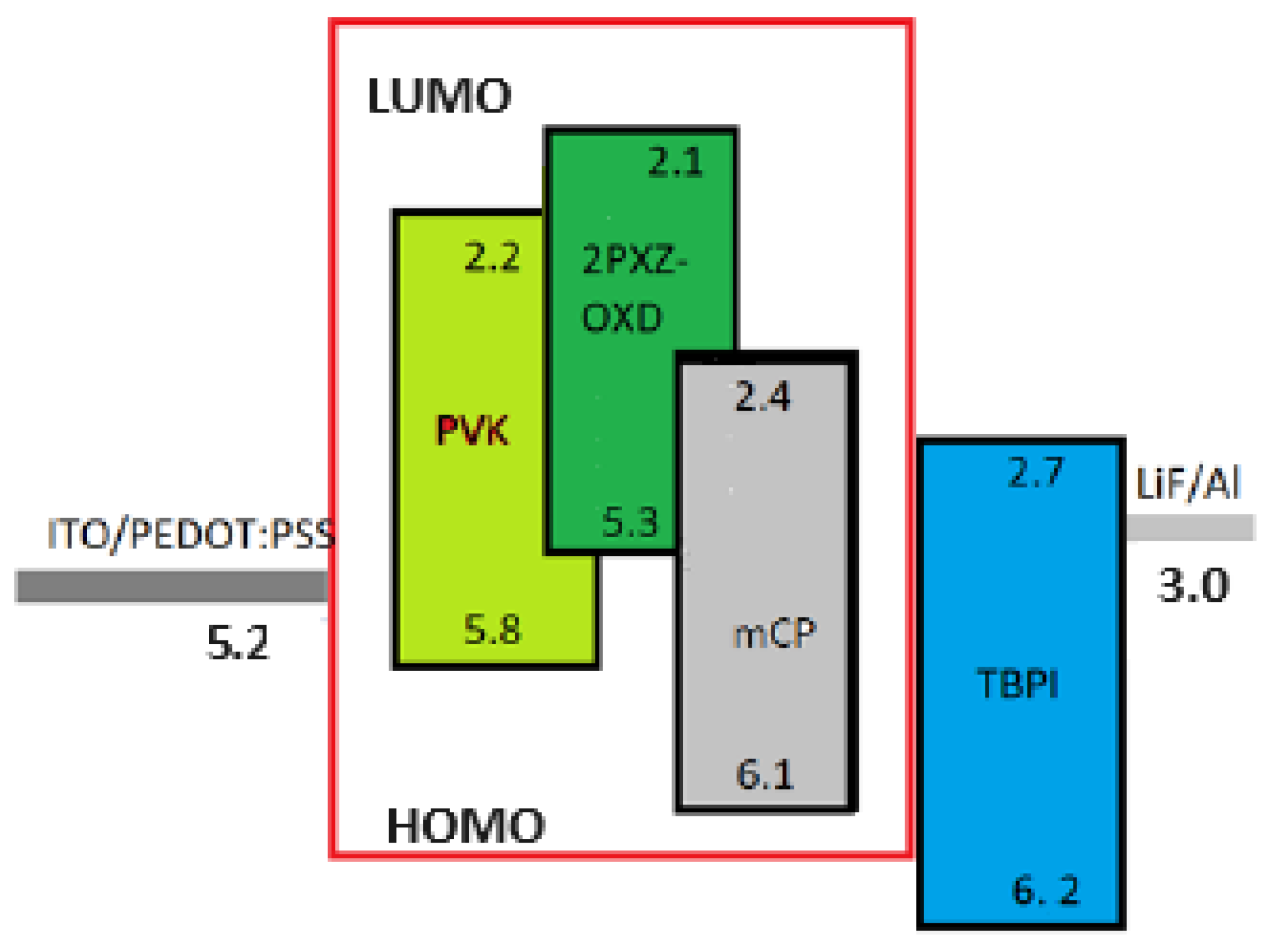
Single-carrier diodes were assembled with the following architecture: ITO|PEDOT:PSS|PVK:mCP:2PXZ-OXD|PEDOT:PSS|Al and ITO|LiF|PVK:mCP:2PXZ-OXD|LiF|Al for the only hole and electron transport, respectively. Conditions of the film deposition, thermal evaporation of LiF and Al, and the J-V measurements were the same as electroluminescent diodes. The simple energy band diagram (with optimized anode / cathode work functions and pure organic HOMO / LUMO levels) is shown in Figure 2.

2.4. Devices opto-electrical characterization

The electroluminescent OLEDs current and luminance versus voltage curves (J,L-V) were measured using a Keithley 2425 source meter unit and a Konica Minolta CS110 Luminance Meter coupled to a close-up lens No. 110, ø=40.5 mm, 20-30 cm, in an proper OLEDs sample holder. EL spectra were acquired using a USB4000 Ocean Optics CCD spectrometer. Luminance and EL measurements were obtained from the normal angle concerning the samples. All OLEDs figures of merit (current efficiency – ηC, power efficiency – ηP, and external quantum efficiency – EQE) were calculated considering Lambertian emission from devices. Impedance spectroscopy measurements were employed in a Fluke PM6306 programmable RCL-meter with an AC level of 0.1 V, an internal BIAS of 0 V and frequencies from 100 Hz to 1 MHz. All measurements were made at room temperature.

3. Results and discussion

3.1. Basic photophysycal characterization

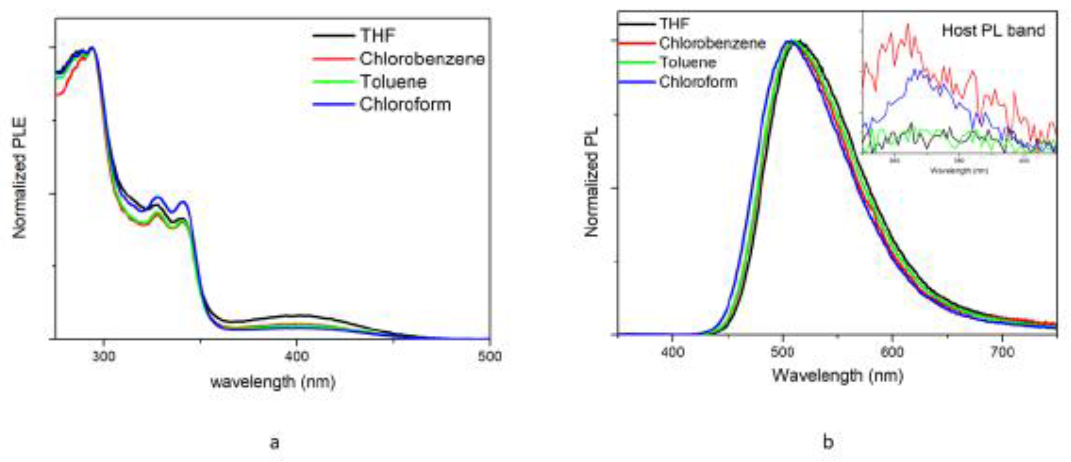
A steady-state photophysical study was carried out in order to help to understand the active layer material solvent effect in the device. The measurements of the TADF used in this work, 2PXZ-OXD, in a matrix of PVK:mCP was evaluated. To obtain the PLE (photoluminescence excited – Figure 3a) spectrum the film is excited with the energy correspondent to the photoluminescent (PL) main peak. After the absorption of this energy the electrons goes to one excited state, and they will relax to an intermediary lower energy state, with a non-radiative transition. After that occurs an emission of a photon with lower energy than the absorbed one. This happen because corresponds to the relaxation from the intermediate state with lower energy to the ground state. The PL spectra of each sample were obtained by using an excitation wavelength of λexc= 290 nm of excitation and its correspondent filter (WG295) to eliminate Rayleigh scattering from the source. This specific λexc can electronically excite the host matrix (PVK:mCP) in contrast to the TADF molecule [37]. Such a strategy is important to evaluate the possible presence of radiative and non-radiative energy transfer processes (trivial and resonant mechanisms, respectively) from the host to the guest molecules. This important feature might impact the EML efficiency in the OLEDs. The non-radiative processes are mainly governate by Forster and Dexter mechanisms, depending only on the excited-state dipole orientation, the spectral overlap of emission and absorption spectra, and the distance between the donor (host) and acceptor (guest) molecules [38]. In addition to the predominance of CT PL band of TADF in the PL spectra of solution-processed EML varying solvent (Figure 3 b), only a small contribution of the host emission (inset Figure 3 b), even electronically exciting the host matrix. Clear evidence of the predominant non-radiative (resonant) energy transfer (RET) process from the PVK:mCP to the 2PXZ-OXD. Looking for the PLE spectra (Figure 3a) monitoring the TADF emission band (500 nm), we can prove the presence of such RET process among host-guest systems in the EML. We observe the characteristic CT excitation band of 2PXZ-OXD molecules around 400 nm, with a minimal intensity when compared to the excitation bands of the PVK polymer: λexc = 341 nm, 328 nm, and 294 nm, which is assigned to the S0 → S1, S0 → S2 and S0 → S3 PVK singlet electronic transitions [39]. These observations do not prove, but it is excellent evidence that our active layers are well organized morphologically at the molecular level. Despite the existence of a little redshift in the PL spectrum, this is not very significant because the difference between them is only around 8nm, so it is considered that the use of different solvents will not have an impact in the energy transfer process.

3.3. Electrical behavior: Current density – Applied voltage – Bright and eficiencies

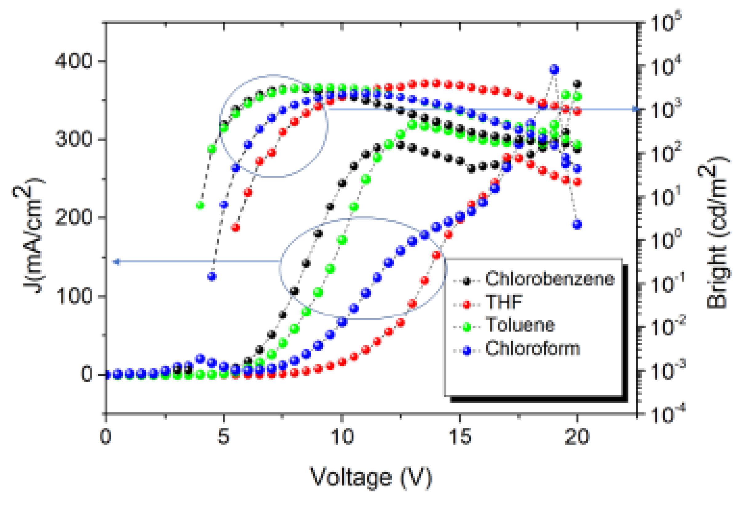
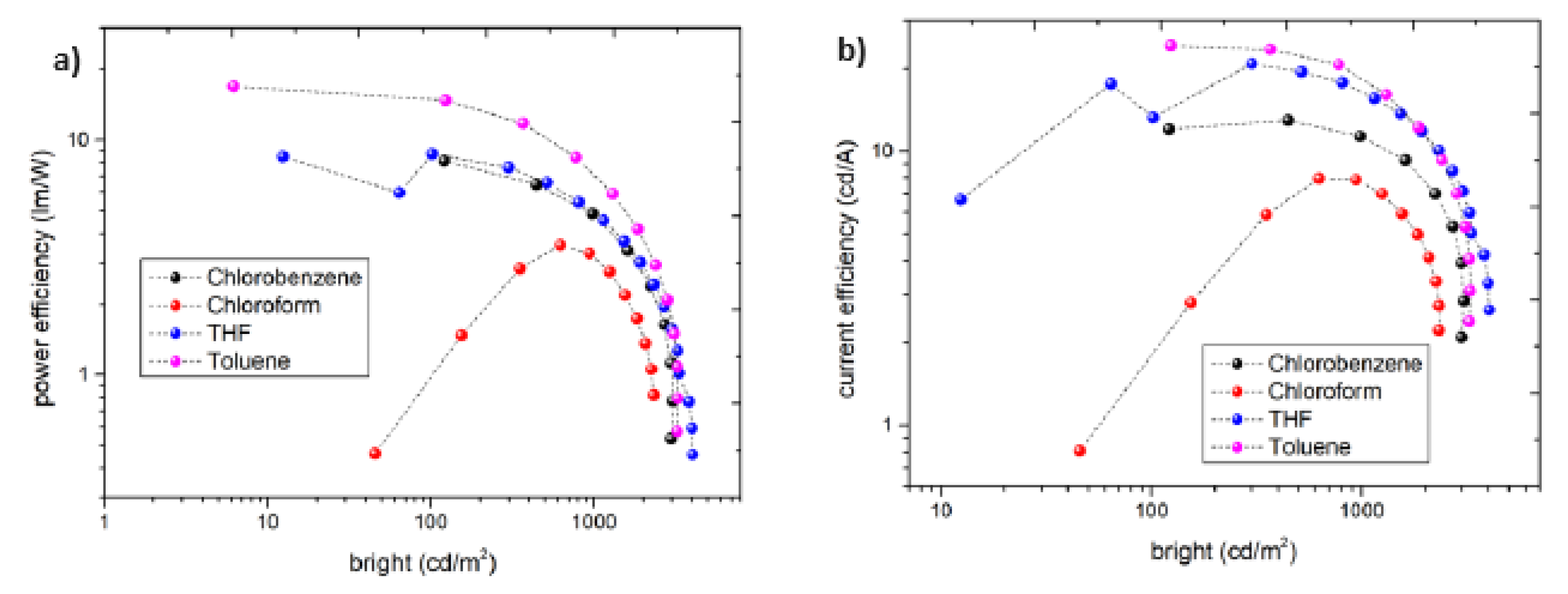
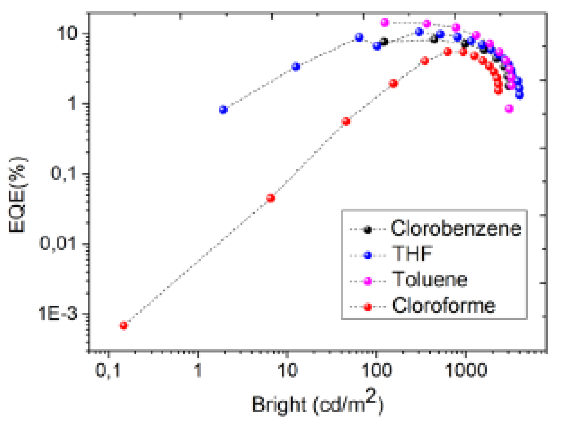
The J-V-L data fir all kind of samples are shown in Figure 4. From the J-V-L data it is possible to see that all devices shown a very low turn on voltage (Von), between 4 and 5 V, a remarkable performance for a simple two organic layer structure. The devices where were used THF as solvent for the active layer materials shown one of the best results (in average). The maximum bright was about 4030 cd m−2, the maximum EQE was 10.5 %, the ηcmax was 20.0 cd A−1, very close to the best device, and the ηpmax was 8.7 lm W−1. The devices (again in average) with the best results were the one where was used toluene as solvent for the active layer materials. This shows a maximum bright of 3240 cd m−2, a ηcmax of 24.3 cd A−1, ηpmax of 16.9 lm W−1 and maximum of EQE of 14 %, this efficiency is very good and is very close to the best in the literature [40]. This one corresponds to a fully evaporated device with a structure that is more complex, with blocking layers. Looking, to these results it is possible to see that the device where was used toluene as solvent for the active layer shows the lowest Von and the best equilibrium between the current efficiency and the power efficiency. These equilibrium results in a EQE of 14%, value very good enough for this type of device structure.
In opposition, the device where was used chloroform as solvent for the active layer shows a current efficiency of only 3.7 cd A−1, a power efficiency of 7.9 lm W−1, a maximum bright of 2330 cd m−2 and a Von of 5 V. This device shows the lowest maximum EQE about 5.5 %. The overall efficiency data are shown in Figure 5.
Finally, in Figure 6, the EQE is shown (also as a dependence on bright). Is should be noted that, instead the usual behavior of the simple OLED device structure, made by solution deposited shown, we achieved a particular interesting low roll-off) when we analyze the EQE, at maximum bright and at 1000 cd cm-1. The lower roll-off appear in the device where was used chloroform as solvent for the active layer, about 1%. And the device where was used toluene as solvent for the active layer materials was the one who show the worst roll-off, about 32 %. In the bright region analyzed, the OLED where was used THF as solvent for the active layer materials showed a roll-off of 25 % and the device where was used chlorobenzene as solvent for the active layer materials showed a roll-off of 6 %. With these results we can observe that until the 1000 cd m−2 these devices are very stable, and we are no employing and blocking layers. These values also show that the device can support the increase in the applied voltage reaching high bright values with stability. Moreover, compared with some performance reported in the literature, based on such TADF emitter but with much complex structure (and with organic layers thermally evaporated, decreasing clearly the structural defects formed), we are running at the edge as much as possible. A deeper discussion will be made further ahead.

3.3. Electroluminescence and color coordinates

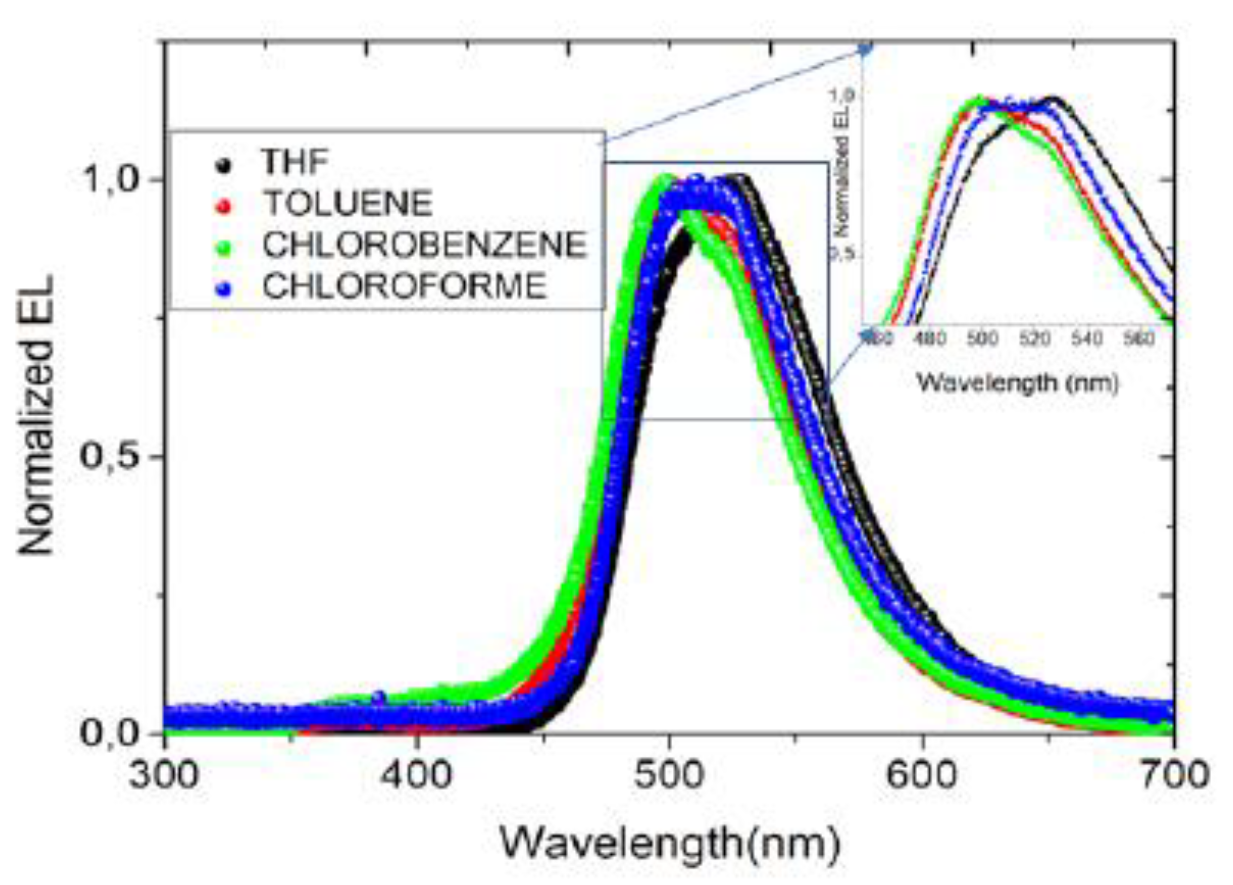
The electroluminescence (EL) spectrum for the OLEDs made with different solvents for the active layer are shown Figure 7. In the EL is possible to see that exists two peaks for the devices made using as solvent the THF and chloroform and three peaks for chlorobenzene and toluene. The first peak that appears in the spectrum for the chlorobenzene and toluene about 380 nm, corresponds to the well-known PVK emission [41, 42], that causes a blue shift in the device emission with these solvents. The origin of this peaks is related to the absolutely incomplete charge transferred from PVK to 2PXZ-OXD. Since this spectrum was taken at 10 V, the electrical charge density is particularly high in the active layer and PVK starts to emit.
The spectrum for THF shows a central peak at 525 nm and a secondary peak at 492 nm. For the chlorobenzene spectrum the principal peak appears at 499 nm and the secondary peak appears at 532 nm, this indicates that exists a blueshift for this solvent that is provoked by the PVK emission. The spectrum obtained for toluene shows a central peak at 498 nm and a secondary peak at 520 nm. For last, the spectrum obtained for chloroform have two peaks that are very close that seems there is only one, the first and principal peak appears at 507 nm and the secondary peak appears at 526 nm. The principal peak in these spectra correspond to the TADF emission. The secondary peak is associated with a non-planar vibration that happens in the oxazole group [43]. This molecular vibration can be symmetric or anti-symmetric, and this will be the key for the difference in the intensity of this molecular vibration, so if the vibration is anti-symmetric the intensity will be lower than the symmetric vibration. Looking to the data obtained in this spectrums is possible to see that the use of different solvents changes the EL emission. This shift also indicates that the solvent will act in the recombination and charge transport mechanisms.
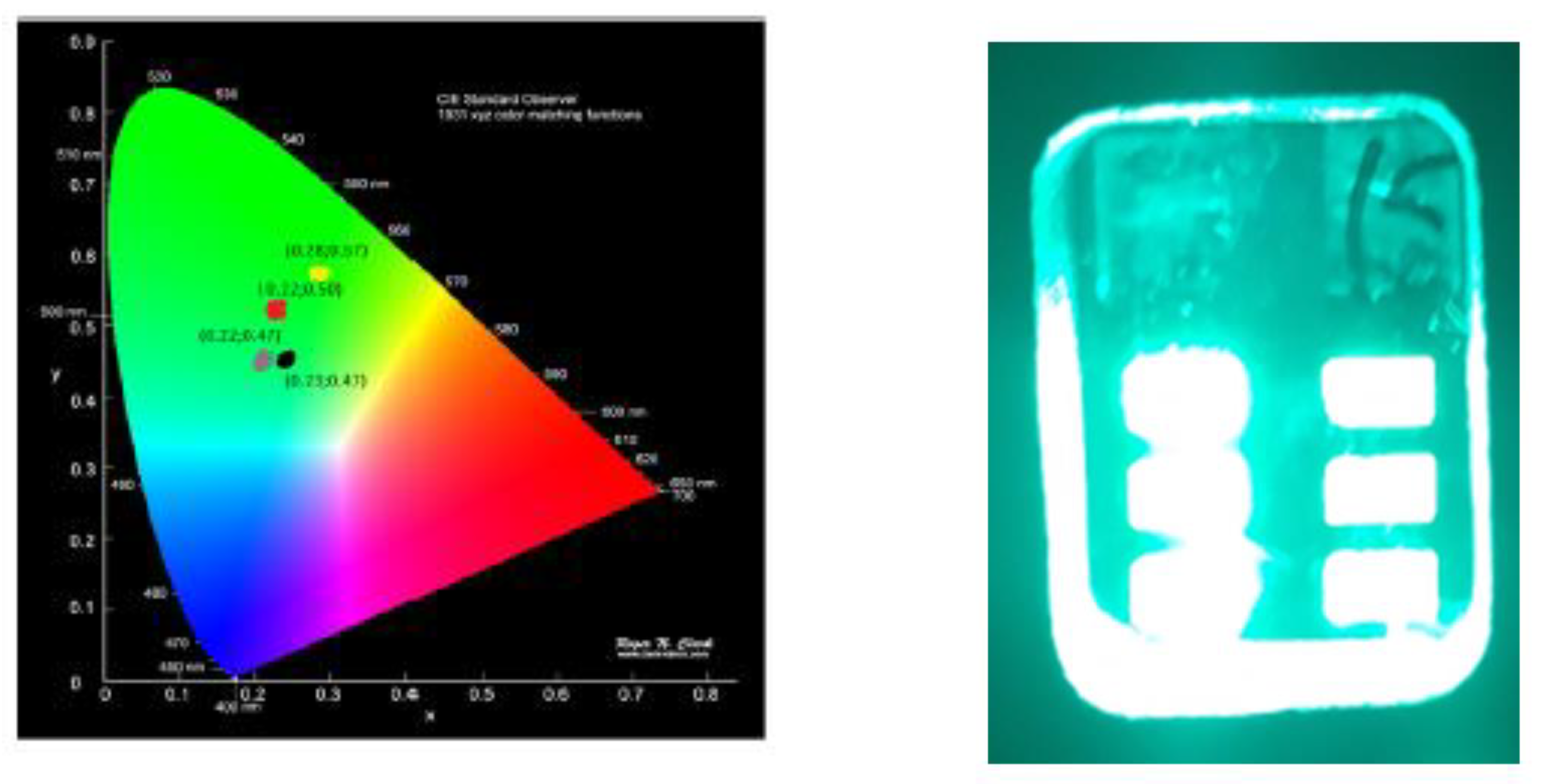
In Figure 8 is possible to see the color coordinates for every OLED with different solvents that was used in the active layer.
Joining the CIE color coordinates information with the EQE behavior (with bright), is naturally observed that the different solvents provoke changes in the color coordinates. If we go from THF to chlorobenzene and chloroform it is possible to see that exists a blueshift in the color coordinates. This can be an indication that the different solvents will make different changes in the molecular conformation. These modifications can be an indication that the use of different environments, in our case solvents, can result in a modification in the molecular conformation, and these changes can be provoked by the different polarity in the environment. A first summary of these data is shown in Table 1.
A detailed study about the charge transport mechanisms on these devices was performed. For this purpose, p- and n- type only devices were made. The p-type device had the follow structure: ITO/PEDOT:PSS/EML/PEDOT:PSS/AL and the n-type device had a similar structure but with LiF replacing the PEDOT:PSS layers.
Considering the usual SCLC model previous described elsewhere [35, 44], we can extract valuable information regarding the electrical parameters involved in the electrical carriers’ transport, namely, the Nt correspond to the density of traps, Et to the energy of traps, μh to the hole mobility and μe to the electron mobility. Table 2 summarizes these data.
Looking to the Table 2 is possible to see that the OLED where was used THF as solvent for the active layer materials shows the best equilibrium between the mobility of electrons and holes, being this situation the most close to the ideal one. Ideally both mobilities should be in same order of magnitude. In this case, we can consider that the recombination will happen in the middle of the active layer (and taking into account the p- and n- type organic stack layer thickness). However if this not happens and there is a big difference between the mobilities the recombination can takes place outside of the active layer, with further loss of efficiency. This device also have a very good equilibrium for the energy of the traps for both charge carriers. However, the best efficiency was obtained for the OLED with the active layer deposited from a solution with toluene. Clearly, the best electrical carrier balance will depend also on different factors, particularly the defect densities and their energy levels. Additionally, the charge transport results also confirm that the OLED where was used chloroform as solvent for the active layer is the worst device. This device, shows the best mobility for holes, but there is a difference of three orders of magnitude between the mobility of electrons and holes. Finally for the OLED where was used chlorobenzene for the active layer the results are in general like the ones for toluene. But in this case exists high trap densities. The energy of the traps for holes is about four times bigger than the energy of the traps for electrons.
In a first summary, the data presented in this section shows that the solvent used in the active layer will make modifications on the charge transport mechanisms. This results can be used to explain some differences between the efficiencies for the OLEDs with different solvents, but they also open some questions about this differences that cannot be answer only with these data. This results also shows that the environment polarization can be changed by the molecular conformity. This one may be changed by the different type of solvent. Finally, this modification may originate the Triple Triplet annihilation (TTA).

3.4. Impedance spectroscopy characterization

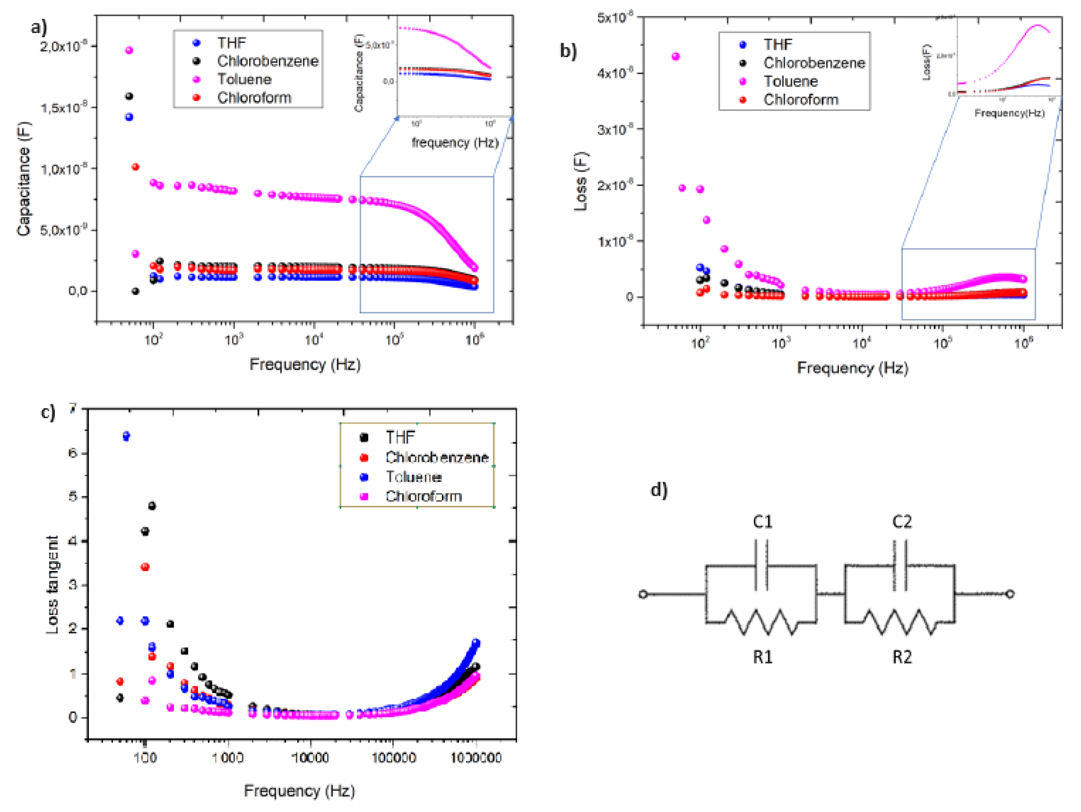
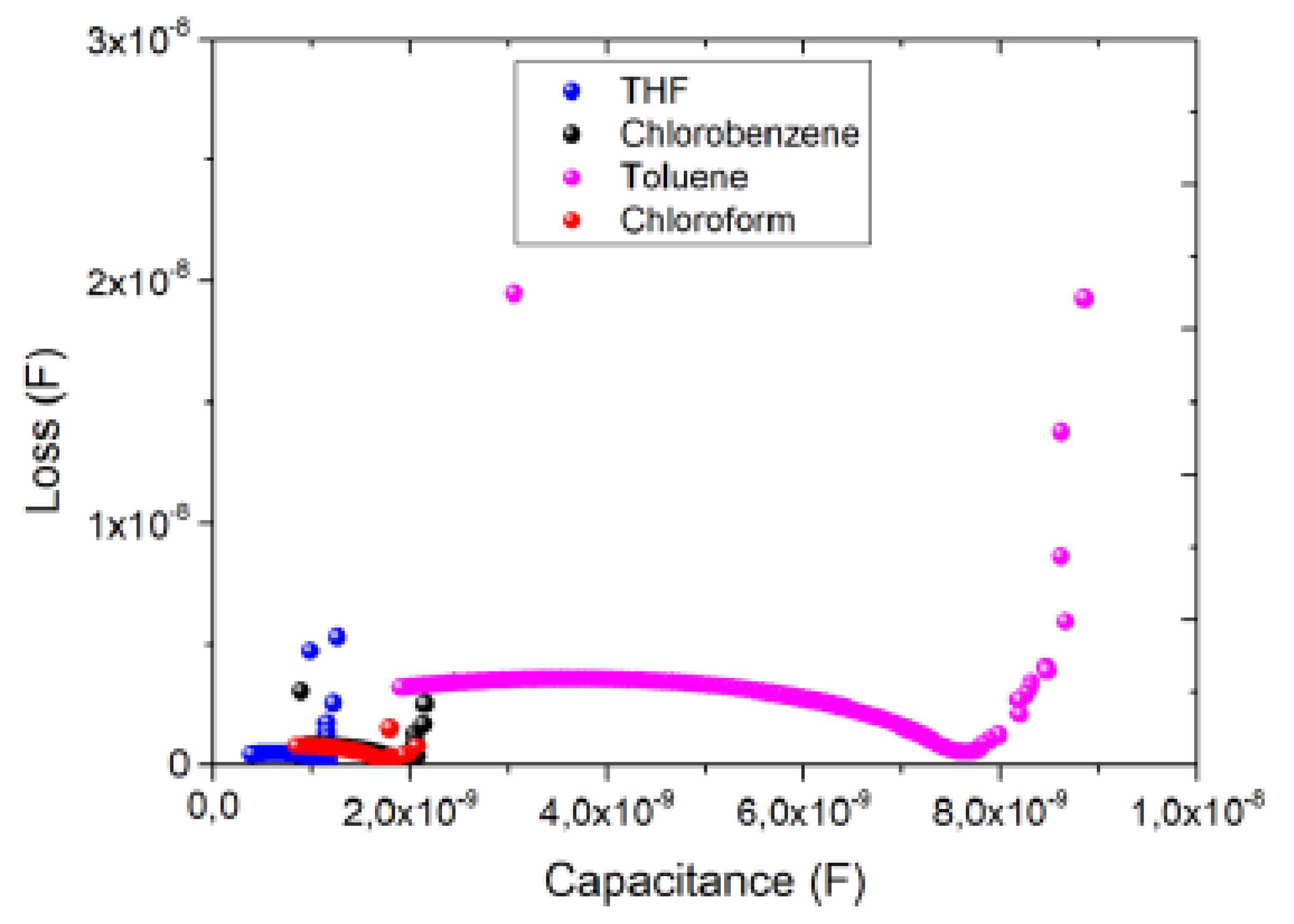
In order to get more insight about differences in the electrical properties observed in the different solution-deposited OLEDs active layers, the measurements in AC domain permits to make a more complete device characterization giving more details about the different electrical transport (and eventually injection at any interface) properties in the OLED. In this part is carried out a study of the capacitance, loss and loss tangent evolution with frequency and the loss evolution with capacitance. Figure 9 shows the plot for capacitance, loss and loss tangent vs frequency for all different king of devices.
As previous referred, all the measurements were made at ambient temperature, with an AC level of 0.1 V, an internal bias of 0 V and a range of frequencies from 100 Hz to 1 MHz. From the data, is possible to obtain the Cole-Cole plot that is composed by the loss in function of the capacitance. Figure 10 is composed by one decreasing part for lower frequency and a semicircle for medium to high frequency. This figure is typical for a potential barrier with an interface and bulk zone. Associating, this with the double relaxation process, that is the typical behavior of a double parallel RC. One should be associated with any potential barrier and the other is associated with the semiconductor bulk (due to the differences observed and compared with the OLEDs figures of merit, should be in the active layer). However, we can´t exclude different physicals process that can imply more complex equivalent circuits. So, considering the degree of freedom that circuit modulation gives, it is necessary to guarantee that the chosen models represent in the right way the physical processes that happens in the device. In this way it was decided to utilize the most simple solution, the double RC parallel circuit, as seen in Figure 9d. For this circuit the parallel capacity is given by:
C p = C g + C 0 C g 1 + ω Γ 2 ,
where
C g = C 1 C 2 C 1 + C 2 ,   C 0 = C 1 R 1 2 + C 2 R 2 2 R 2 + R 1 2 ,   Γ = R 2 R 1 R 1 + R 2 C 2 + C 1
The above equations can be easily obtained from the equivalent electrical circuit resolution shown in Figure 9d. It should be noted that the usual series resistance RS, is not represented here and, for all the OLEDs studied, the values are around 1kΩ, more specifically changing in a suitable and assertive way with the OLEDs figures of merit.
Analyzing all the AC data, it is observed that for the frequency where the capacity starts to drop the loss curve and the loss tangent curve starts to increase. This drop on the capacity reflects a drop in the charges that can follow the AC signal and the system starts to lose the capability to polarize. When the loss curve arrives to the maximum point the loss tangent curve continuous to increase and the capacitance curve decrease. This dropping region, can have a correspondence in the Cole-Cole plot. The corresponding region is the region where happens the second relaxation. This goes along with the theoretical model that was presented for the double RC circuit that was chosen to be the equivalent circuit that better describes the data obtained.
Looking to the obtained results for the capacity and loss is possible to see that the system will have a relaxation for low frequency and another relaxation for high frequency. For the capacitance plot is seen that there is a gradual decrease with frequency increase, until near 105 Hz. This happen because the frequency is starting to get high, and the charges start to show some resistance to follow the AC signal. For this frequency there is a relaxation peak for every device, but for the OLED where was used toluene as solvent for the active layer this decrease is higher than in the other solvents. In the OLED where was used toluene as solvent for the active layer showed the biggest drop in the capacity value. These drops can be (even indirectly) correlated with the charges’ lower mobility, because the charge will have more difficult to follow the AC signal. In opposition, the devices where were used THF and chloroform as solvent for the active layer had a low drop in the capacity value. Which can correspond to a lower charge difficult to follow the AC signal. The OLED where was used chlorobenzene as solvent for the active layer also has a very low drop. The loss plot also shows a decrease with the frequency increase. But between the 104 Hz and 105 Hz there is an increase in the loss plot until reaching the relaxation peak. In the inset plot of Figure 9a/b, is possible to see that this peak appears in different frequencies. For toluene the peak appears near 5.9×10⁵ Hz, for chlorobenzene near 6×10⁵ Hz, for chloroform near 9.9×10⁵ Hz and for THF at frequencies higher than the ones measured. From the loss tangent plot, the behavior for every solvent is very similar, and goes along with the theoretical models presented before. The peak, for high frequencies, corresponds to the point where the capacity stars to decrease. However, there isn´t any visible peak of relaxation. In the Cole-Cole plot is possible to see again the double relaxation process. There are remarkable differences among the devices, however the devices where were used chlorobenzene and chloroform for the active layer show the same behavior.
After making all these assumptions about the physical phenomena that happens inside the device is also important to make the correlation between the data obtained and the physical models considered for the equivalent circuit. So, examining the model considered for the data analyze, is possible to see that for low frequencies the equation will go to a constant value that is given by C0. That value will have a dependence on the capacitances and resistances. For high frequencies the equation will go for another constant value, Cg, that only depends on both capacitances. Both of this constants don´t have a frequency dependence. With the association of the experimental data with this model is possible obtain the values for the resistances and capacitances, that can provide more information about the way that charge will flow and will accumulate in the layer.
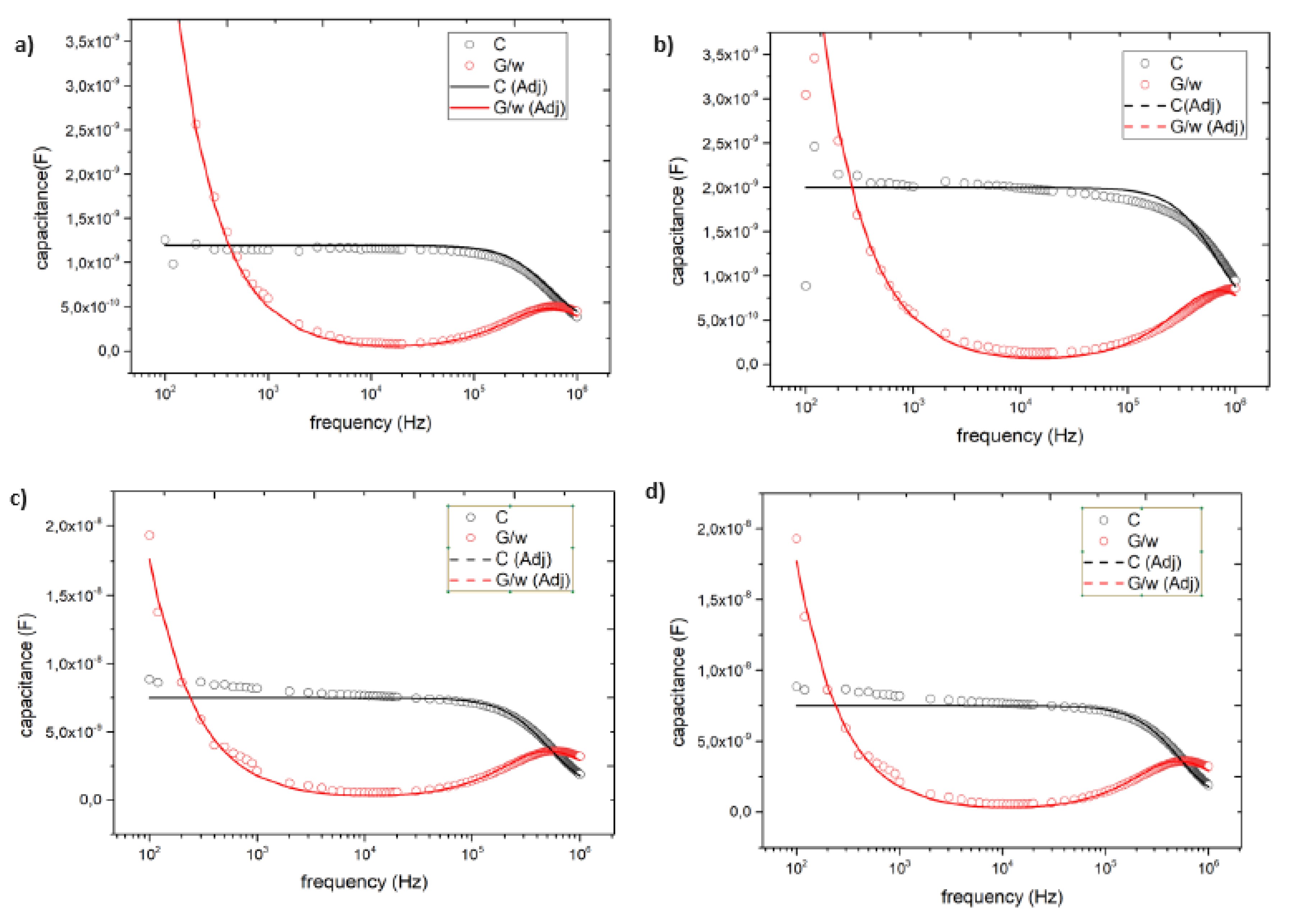
A fully simulation of the equivalent electrical circuit can be done (numerical convergence methods), in order to extract the physical data of the circuit. The next figure (Figure 11) shows such numerical fits.
Looking for these curves is possible to see that in every OLED for high frequencies the model is well adjusted to the experimental data. For The OLED where was used chlorobenzene as solvent for the active layer at medium frequencies there is a little discrepancy between the simulated curve and the experimental data. This discrepancy can be related with some physical phenomena that can happen in the device for these frequencies. Also, exists a discrepancy between the simulated curve and the experimental data at low frequencies. This can be correlated with the equipment limitations at low frequency.
However, we cannot eliminate the existence of other physical phenomena that can happen in the devices. In Table 3 are presented the values obtained for the capacitances, resistance and relaxation times for the equivalent circuit considered for the data analyze and simulations.
With this equivalent circuit is possible to consider that, in our case, the first circuit (R1 and C1) can be related with any interface (although other effects are not out of consideration) and the second circuit (R2 and C2) can be related with the bulk. In this table is possible to see that the OLED where was used toluene as solvent for the active layer is the one with highest C1 value. Since the capacity is a measure of the charge accumulation, this may indicate that, in this OLED, the interface can accumulate more charge than in the other devices. Additionally, this device also shows the highest relaxation time. The OLED where was used THF for the active layer was the one who showed the lower value for C1. So, if this device has lower capacity this can give an indication about the lower charge accumulate in the interface. The lowest relaxation time for the interface appeared in the OLED where was used chlorobenzene for the active layer. This one also showed the second lower capacitance. Taking into account now the other RC circuit is possible to see that the capacitance values, C2, are much lower than the ones for the interface region. Normally, the recombination phenomena happen in this region. With this is expected to have a lower charge accumulation, since the majority of the charges are recombining. So, if we have high values for the capacity this can indicate that there is more charge accumulation. And if we have more charge accumulation, the charges that are recombining will be lower. The values for C2 are very close but there is a little shift for the OLED where was used chloroform and chlorobenzene as solvents for the active layer. The OLED where was used chlorobenzene for the active layer is the one with lower C2 values. Since this value gives an indication about the charges that are accumulated in this region. The lower value can be a indication about the lower charge accumulation and consequently more charges for the recombination process. The OLED where was used toluene as solvent for the active layer also have lower C2 values, this goes along with the results for the EQE presented in the previous sections, because in this device there is lower charge accumulation and there are more charges for the recombination process. For the other side the OLED where was used chloroform as solvent for the active layer is the one with higher C2 values. The fact that this value is a little higher than the ones for the other devices can give an information about the fact that the charge accumulation is higher and per consequence the charges for the recombination process will be lower. The second relaxation time presented in this table corresponds to the relaxation that appear for higher frequencies in the capacitance and loss plots. This relaxation phenomena can be related with the physical properties of the active layer.
The existence of traps in the devices implies that exists a finite time for the charge interaction with electrically active levels (some certainly arising from defects). So, the device with lower relaxation time is the one that used toluene for the active layer and the device with higher relaxation time, for the high frequency relaxation, is the one that used THF as solvent for the active layer. Considering these results is possible to make the assumption that in the OLED where was used toluene for the active layer the charge interaction with the traps possibly is lower than in the other devices.
In summary, with every consideration made, it is possible to conclude that the solvent will induce changes in the molecular conformation. If we look to the guest:host energy transfer process the photophysical measures gives an indication that the solvent will not induce changes, and, therefore, the electrical charge transport and accumulatio, needs to be the fundamental explanation for the differences obtained. Finally, from the impedance spectroscopy is possible to conclude that exists differences in the charge accumulation and in the interaction time between the charges and the trap levels, thar are consequence of the different molecular conformation at active layer as a result of different solution properties employed in the deposition, Therefore, a correct choice of the solvent appears to be one way to Furter exploration.

5. Conclusions

This work, aimed to develop and characterize OLEDs based on a 2PXZ-OXD green TADF, in simplified structures (two organic layers), and their optimization in terms of efficiency in a trade-off between both objectives. The work involved the wet manufacturing of OLEDs (spin-coating) and the electro-optical characterization giving the figures of merit based on the applicable physical models for the injection / transport and recombination of electrical charge. At the same time, it was intended that the emitter layer maintain the best possible molecular conformation.
From the analysis of the figures of merit it was possible to see that the best device was the one that used toluene as solvent for the active layer with figures of merit near of the best reported in the literature but with a more complex device structure. This maximum bright was 3240 cd.m−2, ηc,max of 24.3 cd.A−1, ηp,max of 16.9 lm.W−1 and a maximum EQE of 14%. For the other side the worst device was used chloroform as solvent. By DC electrical characterization, was possible to correlate the data with intrinsic defects formation and electrical balance of the carriers inside active layer.
By impedance spectroscopy we conclude that that the system can be modulated by two RC parallel circuit in series. The capacitance vs frequency plot shown differences for the four types of OLEDs, one factor that can explain these differences is the charge mobility in the device. With the fitting curves was possible to obtain the parameters to describe the equivalent circuit that was considered for the data analysis. A relationship between relaxation times and pure figures of merit, cab be obtained, helping on a better understand of the molecular conformation differences in the OLED active layer, opening new opportunities for further developments.

Author Contributions

“Conceptualization, L.P; methodology, F.T, J.G and L.P.; software, NA, validation, , F.T, J.G and L.P.; formal analysis, .T, J.G and L.P., investigation, F.T, J.G and L.P.; resources, L.P.; data curation, ------, writing—original draft preparation, F.T, J.G and L.P..; writing—review and editing, J.G and L.P.; visualization, , F.T, J.G and L.P., supervision, J.G and L.P.; project administration, L.P., funding acquisition, L.P. All authors have read and agreed to the published version of the manuscript.”.

Funding

F.M.T.: J.C.G. and L.P. acknowledge Institute for Nanostructures, Nanomodelling and Nanofabrication (i3N), Portuguese Foundation for Science and Technology (FCT) (UIDB/50025/2020 & UIDP/50025/2020). J.C.G. also thanks FCT/i3N/UA for the individual CEEC grant (2021.02056.CEECIND).

Data Availability Statement

We encourage all authors of articles published in MDPI journals to share their research data. In this section, please provide details regarding where data supporting reported results can be found, including links to publicly archived datasets analyzed or generated during the study. Where no new data were created, or where data is unavailable due to privacy or ethical restrictions, a statement is still required. Suggested Data Availability Statements are available in section “MDPI Research Data Policies” at https://www.mdpi.com/ethics.

Conflicts of Interest

The authors declare no conflict of interest.

References

  1. Tang, C. W.; Vanslyke, S. A. Organic Electroluminescent Diodes. Appl. Phys. Lett. 1987, 51(12), 913–915. [Google Scholar] [CrossRef]
  2. Hong, G.; Gan, X.; Leonhardt, C.; Zhang, Z.; Seibert, J.; Busch, J. M.; Bräse, S. A Brief History of OLEDs—Emitter Development and Industry Milestones. Adv. Mater. 2021, 33 (9). [CrossRef]
  3. Minotto, A.; Bulut, I.; Rapidis, A. G.; Carnicella, G.; Patrini, M.; Lunedei, E.; Anderson, H. L.; Cacialli, F. Towards Efficient Near-Infrared Fluorescent Organic Light-Emitting Diodes. Light Sci. Appl. 2021, 10(1), 18. [Google Scholar] [CrossRef] [PubMed]
  4. Shin, H.; Lee, J.-H.; Moon, C.-K.; Huh, J.-S.; Sim, B.; Kim, J.-J. Sky-Blue Phosphorescent OLEDs with 34.1% External Quantum Efficiency Using a Low Refractive Index Electron Transporting Layer. Adv. Mater. 2016, 28 (24), 4920–4925. [CrossRef]
  5. Wong, M. Y.; Zysman-Colman, E. Purely Organic Thermally Activated Delayed Fluorescence Materials for Organic Light-Emitting Diodes. Adv. Mater. 2017, 29(22), 1605444. [Google Scholar] [CrossRef]
  6. Liu, D.; Tian, W.; Feng, Y.; Zhang, X.; Ban, X.; Jiang, W.; Sun, Y. Achieving 20% External Quantum Efficiency for Fully Solution-Processed Organic Light-Emitting Diodes Based on Thermally Activated Delayed Fluorescence Dendrimers with Flexible Chains. ACS Appl. Mater. Interfaces 2019, 11(18), 16737–16748. [Google Scholar] [CrossRef]
  7. Li, C.; Xu, Y.; Liu, Y.; Ren, Z.; Ma, Y.; Yan, S. Highly Efficient White-Emitting Thermally Activated Delayed Fluorescence Polymers: Synthesis, Non-Doped White OLEDs and Electroluminescent Mechanism. Nano Energy 2019, 65 (June). [CrossRef]
  8. Liu, H.; Fu, Y.; Chen, J.; Tang, B. Z.; Zhao, Z. Energy-Efficient Stable Hyperfluorescence Organic Light-Emitting Diodes with Improved Color Purities and Ultrahigh Power Efficiencies Based on Low-Polar Sensitizing Systems. Adv. Mater. 2023, 35 (22). [CrossRef]
  9. Bian, M.; Zhang, D.; Wang, Y.; Chung, Y.-H.; Liu, Y.; Ting, H.; Duan, L.; Chen, Z.; Bian, Z.; Liu, Z.; Xiao, L. Long-Lived and Highly Efficient TADF-PhOLED with “(A) n –D–(A) n ” Structured Terpyridine Electron-Transporting Material. Adv. Funct. Mater. 2018, 28(28), 1800429. [Google Scholar] [CrossRef]
  10. Sun, J. W.; Lee, J.-H.; Moon, C.-K.; Kim, K.-H.; Shin, H.; Kim, J.-J. A Fluorescent Organic Light-Emitting Diode with 30% External Quantum Efficiency. Adv. Mater. 2014, 26(32), 5684–5688. [Google Scholar] [CrossRef]
  11. Ban, X.; Chen, F.; Pan, J.; Liu, Y.; Zhu, A.; Jiang, W.; Sun, Y. Exciplex Formation and Electromer Blocking for Highly Efficient Blue Thermally Activated Delayed Fluorescence OLEDs with All-Solution-Processed Organic Layers. Chem. - A Eur. J. 2020, 26 (14), 3090–3102. [CrossRef]
  12. Tian, Q. S.; Shen, W. S.; Yu, Y. J.; Wang, X. Q.; Cai, J. H.; Hu, Y.; Jiang, Z. Q.; Huang, J. S.; Liao, L. S. Systematic Strategy for High-Performance Small Molecular Hybrid White OLED via Blade Coating at Ambient Condition. Org. Electron. 2022, 100 (September 2021), 106366. [Google Scholar] [CrossRef]
  13. Kant, C.; Mahmood, S.; Katiyar, M. Large-Area Inkjet-Printed OLEDs Patterns and Tiles Using Small Molecule Phosphorescent Dopant. Adv. Mater. Technol. 2023, 8 (5). [CrossRef]
  14. C, A.; Dubey, D. K.; Pahlevani, M.; Welch, G. C. Slot-Die Coating of All Organic/Polymer Layers for Large-Area Flexible OLEDs: Improved Device Performance with Interlayer Modification. Adv. Mater. Technol. 2021, 6 (9). [CrossRef]
  15. Guo, K.; Tang, Z.; Chou, X.; Pan, S.; Wan, C.; Xue, T.; Ding, L.; Wang, X.; Huang, J.; Zhang, F.; Wei, B. Printable Organic Light-Emitting Diodes for next-Generation Visible Light Communications: A Review. Adv. Photonics Nexus 2023, 2(04), 1–14. [Google Scholar] [CrossRef]
  16. Kim, H. J.; Godumala, M.; Kim, S. K.; Yoon, J.; Kim, C. Y.; Park, H.; Kwon, J. H.; Cho, M. J.; Choi, D. H. Color-Tunable Boron-Based Emitters Exhibiting Aggregation-Induced Emission and Thermally Activated Delayed Fluorescence for Efficient Solution-Processable Nondoped Deep-Blue to Sky-Blue OLEDs. Adv. Opt. Mater. 2020, 8(14), 1–9. [Google Scholar] [CrossRef]
  17. Cariati, E.; Lucenti, E.; Botta, C.; Giovanella, U.; Marinotto, D.; Righetto, S. Cu(I) Hybrid Inorganic–Organic Materials with Intriguing Stimuli Responsive and Optoelectronic Properties. Coord. Chem. Rev. 2015, 306, 566–614. [Google Scholar] [CrossRef]
  18. Liang, X.; Tu, Z. L.; Zheng, Y. X. Thermally Activated Delayed Fluorescence Materials: Towards Realization of High Efficiency through Strategic Small Molecular Design. Chem. - A Eur. J. 2019, 25 (22), 5623–5642. [CrossRef]
  19. Naveen, K. R.; Yang, H. I.; Kwon, J. H. Double Boron-Embedded Multiresonant Thermally Activated Delayed Fluorescent Materials for Organic Light-Emitting Diodes. Commun. Chem. 2022, 5(1), 1–14. [Google Scholar] [CrossRef] [PubMed]
  20. Yuan, W.; Hu, D.; Zhu, M.; Shi, W.; Shi, C.; Sun, N.; Tao, Y. Simple Peripheral Modification for Color Tuning of Thermally Activated Delayed Fluorescence Emitters in OLEDs. Dye. Pigment. 2021, 191 (April), 109395. [Google Scholar] [CrossRef]
  21. Naveen, K. R.; Palanisamy, P.; Chae, M. Y.; Kwon, J. H. Multiresonant TADF Materials: Triggering the Reverse Intersystem Crossing to Alleviate the Efficiency Roll-off in OLEDs. Chem. Commun. 2023, 59(25), 3685–3702. [Google Scholar] [CrossRef]
  22. Fan, X.; Hao, X.; Huang, F.; Yu, J.; Wang, K.; Zhang, X. RGB Thermally Activated Delayed Fluorescence Emitters for Organic Light-Emitting Diodes toward Realizing the BT. 2020 Standard. Adv. Sci. 2023, 2303504, 1–24. [Google Scholar] [CrossRef]
  23. Wang, D.; Zhang, Q. Fundamental Theories of TADF. In Thermally Activated Delayed Fluorescence Organic Light-Emitting Diodes (TADF-OLEDs); Elsevier, 2022; pp 71–89. [CrossRef]
  24. Kumar., Manish, Ribeiro, Miguel and Pereira, Luiz, “New generation of high efficient OLED using Thermally Activated Delayed Fluorescent materials”, in Light-emitting diode: An outlook on the empirical features and its recent technological advancements", InTech Open, 2018, ISBN 978-953-51-5972-8.
  25. Northey, T.; Stacey, J.; Penfold, T. J. The Role of Solid State Solvation on the Charge Transfer State of a Thermally Activated Delayed Fluorescence Emitter. J. Mater. Chem. C 2017, 5(42), 11001–11009. [Google Scholar] [CrossRef]
  26. Phan Huu, D. K. A.; Saseendran, S.; Dhali, R.; Franca, L. G.; Stavrou, K.; Monkman, A.; Painelli, A. Thermally Activated Delayed Fluorescence: Polarity, Rigidity, and Disorder in Condensed Phases. J. Am. Chem. Soc. 2022, 144(33), 15211–15222. [Google Scholar] [CrossRef] [PubMed]
  27. Li, F.; Li, M.; Fan, J.; Song, Y.; Wang, C. K.; Lin, L. Theoretical Study on Thermally Activated Delayed Fluorescence Emitters in White Organic Light-Emitting Diodes: Emission Mechanism and Molecular Design. J. Phys. Chem. A 2020, 124(37), 7526–7537. [Google Scholar] [CrossRef]
  28. Schleper, A. L.; Goushi, K.; Bannwarth, C.; Haehnle, B.; Welscher, P. J.; Adachi, C.; Kuehne, A. J. C. Hot Exciplexes in U-Shaped TADF Molecules with Emission from Locally Excited States. Nat. Commun. 2021, 12(1), 1–9. [Google Scholar] [CrossRef]
  29. Monkman, A. Photophysics of Thermally Activated Delayed Fluorescence. Highly Effic. OLEDs Mater. Based Therm. Act. Delayed Fluoresc. 2018, 425–463. [Google Scholar] [CrossRef]
  30. Eng, J.; Penfold, T. J. Open Questions on the Photophysics of Thermally Activated Delayed Fluorescence. Commun. Chem. 2021, 4(1), 21–24. [Google Scholar] [CrossRef]
  31. Eng, J.; Penfold, T. J. Understanding and Designing Thermally Activated Delayed Fluorescence Emitters: Beyond the Energy Gap Approximation. Chem. Rec. 2020, 20(8), 831–856. [Google Scholar] [CrossRef]
  32. Kumar, M.; Chapran, M.; Wiosna-Sałyga, G.; Sleczkowski, P.; Luszczynska, B.; Pereira, L. An Insight on Charge Transport in High Efficient Green Solution-Processed TADF OLEDs with a Single Emitting Layer. J. Phys. Chem. C 2020. [CrossRef]
  33. Kumar, M.; Pereira, L. Mixed-Host Systems with a Simple Device Structure for Efficient Solution-Processed Organic Light-Emitting Diodes of a Red-Orange TADF Emitter. ACS Omega 2020, 5(5), 2196–2204. [Google Scholar] [CrossRef]
  34. Kumar, M.; Pereira, L. “Towards Highly Efficient TADF Yellow-Red OLEDs Fabricated by Solution Deposition Methods: Critical Influence of the Active Layer”, Nanomaterials 2020, 10, 101. [CrossRef]
  35. Pereira, L. Organic light emitting diodes: The use of rare earth and transition metals; CRC Press: Singapore, 2012. [Google Scholar]
  36. Kumar, Manish and Pereira, Luiz, “Development of Efficient OLEDs from Solution Deposition”, J. Vis. Exp. (189), e61071, 2022. [CrossRef]
  37. Bonon, B. M. A. and Atvars, T. D. Z. “Energy transfer from poly(vinyl carbazole) to a fluorenevinylene copolymer in solution and in the solid state†,” Photochemistry and Photobiology, vol. 88, no. 4, pp. 801–809, 2012. [CrossRef]
  38. Germino, J. C. and Duarte, L. G. T. A. Semiconducting polymers: Synthesis and Photophysical Properties; vol. 1, ch. Photophysics basic concepts, pp. 39–72. Apple Academic Press, 1 ed., 2021.
  39. Germino, J. C. , de Freitas, J. N., Domingues, R. A., Quites, F. J., Faleiros, M. M., and Atvars, T. D. Z. Organic light-emitting diodes based on PVK and Zn(II) salicylidene composites. Synthetical Metals, vol. 241, pp. 7–16, 2018.
  40. Lee, J.; Shizu, K.; Tanaka, H.; Nomura, H.; Yasuda, T.; Adachi, C. Oxadiazole- and Triazole-Based Highly-Efficient Thermally Activated Delayed Fluorescence Emitters for Organic Light-Emitting Diodes. J. Mater. Chem. C 2013, 1(30), 4599. [Google Scholar] [CrossRef]
  41. Knyazev, A. A.; Krupin, A. S.; Romanova, K. A.; Galyametdinov, Y. G. Luminescence and Energy Transfer in Poly(N-Vinylcarbazole) Blends Doped by a Highly Anisometric Eu(III) Complex. J. Coord. Chem. 2016, 69(9), 1473–1483. [Google Scholar] [CrossRef]
  42. Rodríguez-Mas, F.; Ferrer, J. C.; Alonso, J. L.; Fernández de Ávila, S.; Valiente, D. Reduced Graphene Oxide Inserted into PEDOT:PSS Layer to Enhance the Electrical Behaviour of Light-Emitting Diodes. Nanomaterials 2021, 11(3), 645. [Google Scholar] [CrossRef]
  43. NIST, “Oxazole.” https://webbook.nist.gov/cgi/cbook.cgi?ID=C288426&Mask=80, 9. Accessed on 22nd September, 2022.
  44. Lampert, M. A.; Mark, P. Current Injection in Solids; Academic Press: New York, USA, 1970. [Google Scholar]
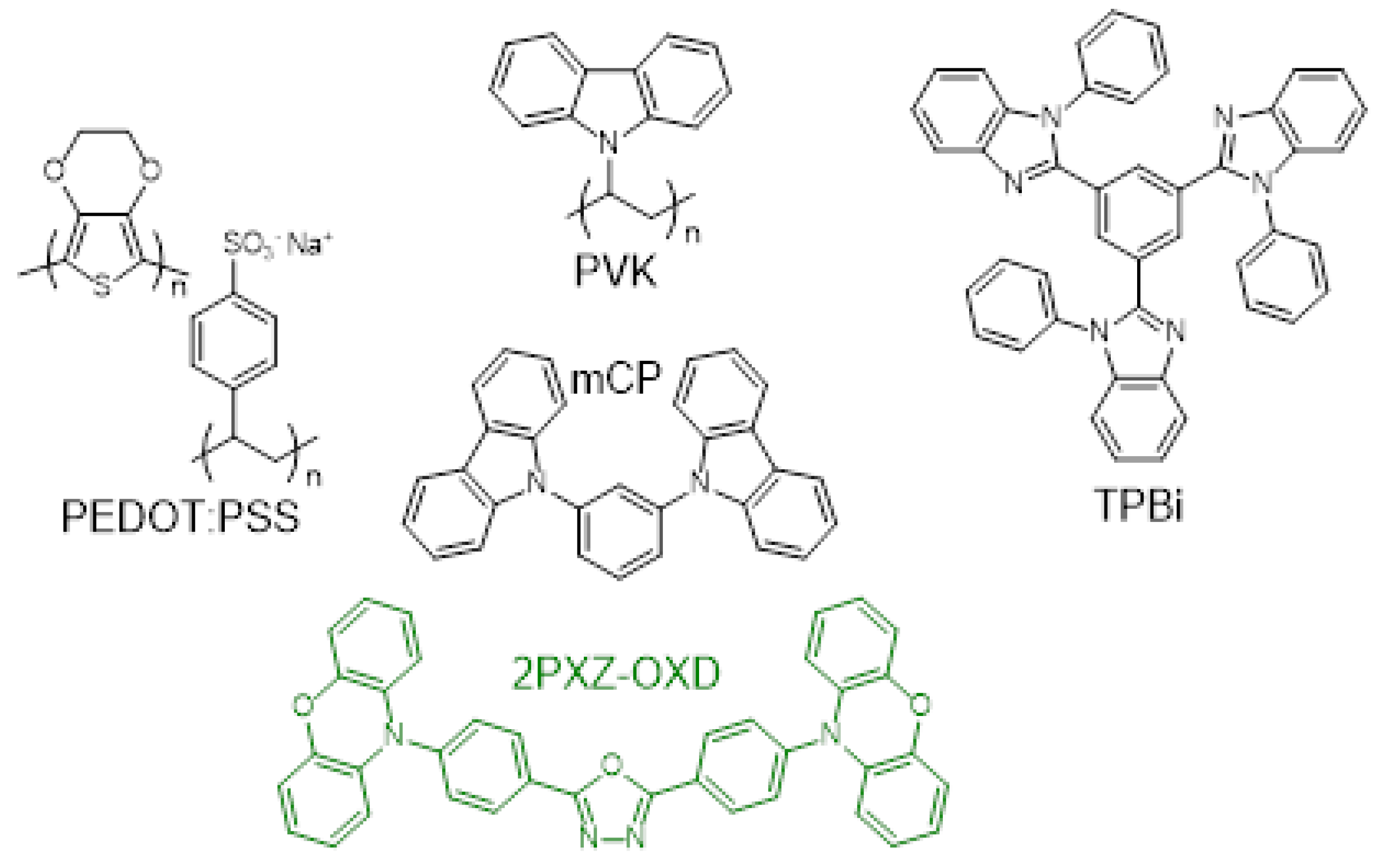
Figure 1. This is a figure. Schemes follow the same formatting.
Preprints 86442 g001
Figure 2. Device energy levels. The organic layers inside the red line, are the constituents of the host (PVK and mCP) and guest (2PXZ-OXD) materials in the matrix. All values are in eV.
Preprints 86442 g002
Figure 3. (a) PLE spectrum for every device obtained with the excitation wavelength corresponding to the central maximum of photoluminescence spectrum (b) Photoluminescence spectrum obtained for every active layer density and bright in function of the applied potential for every OLED made with the different solvents for the active layer.
Preprints 86442 g003
Figure 4. Current density and bright in function of the applied potential for every OLED made with the different solvents for the active layer.
Preprints 86442 g004
Figure 5. (a)Plot of power efficiency and (b) plot of current efficiency in function of the bright for every OLED made with the different solvents for the active layer. The fast decrease observed for bights higher than ≈ 2000 cd m-2, are due to the device irreversible degradation.
Preprints 86442 g005
Figure 6. EQE in function of the bright for the devices.
Preprints 86442 g006
Figure 7. Electroluminescence spectrum obtained for an applied voltage of 10V for every OLED made with the different solvents for the active layer.
Preprints 86442 g007
Figure 8. CIE chromaticity diagram with the color coordinates for every OLED made with the different solvents for the active layer. The correspondent color coordinates are: (0.23;0.47) for Chloroform (black point), (0.28;0.57) for THF (yellow point), (0.22;0.50) for Toluene (red point) and (0.22;0.47) for Chlorobenzene (grey point). spectrum obtained for an applied voltage of 10V for every OLED made with the different solvents for the active layer. Photo of an OLED working at 10V.
Preprints 86442 g008
Figure 9. data made with the different solvents for the active layer for each kind of OLE: (a) Capacitance vs frequency (b) Loss vs frequency, (c) Loss tangents vs frequency and (d) Equivalent circuit considered for the obtained data analysis.
Preprints 86442 g009
Figure 10. Cole-Cole plot for every OLED made with the different solvents for the active layer.
Preprints 86442 g010
Figure 11. Capacitance(C) and loss(G/ω) data for the different kind of OLEDs fabricated. Open circles: experimental data; lines: fitting using the double RC circuit. (a) THF as solvent, (b) chlorobenzene as solvent, (c) toluene as solvent and (e) chloroform as solvent.
Preprints 86442 g011
Table 1. OLEDs main figures of merit properties.
solvent Von
(V)
Lmax cd.m−2 ηc cd.A−1 ηp lm.W −1 EQEmax
%
EQE (@1000 cd m−2)
%
λcentral
nm
color
coordinate
(x,y)
Toluene 4.0 3270 24.3 16.9 14 9.5 499 0.22, 0.50
THF 5.5 4030 20.0 8.7 10.5 7.9 527 0.28, 0.57
Chlorobenzene 4.5 3060 12.9 8.4 8.2 7.7 498 0.22, 0.47
Chloroform 5.0 2330 3.7 7.9 5.5 4.9 507 0.23, 0.47
Table 2. OLEDs charge transport properties obtained with the SCLC model and the correspondent EQE for comparison purposes.
Solvente Nt (e)
×1017cm−3
Nt
(h+)
×1017cm−3
Et (e)
mEv
Et (h+)
mEv
µe
×10−12
cm2/v.s
µh
×10−9
cm2/v.s
EQE
%
Toluene 5.5 2.5 88.1 46.5 1.0 3.9 14.0
THF 4.6 4.9 61.2 65.8 478.0 5.8 10.5
Chlorobenzene 9.0 8.6 20.0 80.7 9.3 1.9 8.2
Chloroform 6.5 14.8 63.6 82.2 902.0 126 5.5
Table 3. Values obtained with the fittings for the equivalent circuit resistances and capacitances, and the respective times of relaxation.
solvent R1
(KΩ)
C1
(nF)
τ1
(ms)
R2
(Ω)
C2
(nF)
τ2
(ns)
Toluene 90 7.5 0.675 40 0.3 12
THF 320 1.2 0.384 200 0.3 60
Chlorobenzene 750 1.7 0.128 100 0.2 20
Chloroform 300 2.0 0.600 95 0.4 30
Disclaimer/Publisher’s Note: The statements, opinions and data contained in all publications are solely those of the individual author(s) and contributor(s) and not of MDPI and/or the editor(s). MDPI and/or the editor(s) disclaim responsibility for any injury to people or property resulting from any ideas, methods, instructions or products referred to in the content.
Copyright: This open access article is published under a Creative Commons CC BY 4.0 license, which permit the free download, distribution, and reuse, provided that the author and preprint are cited in any reuse.
Prerpints.org logo

Preprints.org is a free preprint server supported by MDPI in Basel, Switzerland.

Subscribe

© 2024 MDPI (Basel, Switzerland) unless otherwise stated