1. Introduction
At the present time, in connection with the further miniaturization of microchips elements, refractory metals and their alloys are used, which are functionally better than traditionally used copper and aluminum. However, the common disadvantage of materials is their lower conductivity and poor adhesion to the semiconductor surface [
1,
2,
3,
4,
5,
6]. Partly, these problems are figure out by applying thin films of Au, Pd and Ag on the surface of refractory metals, or by selecting composite layers from various metals. For these purposes, the method of magnetron sputtering or ion-beam doping is usually used [
7,
8,
9,
10,
11,
12]. However, these metals are expensive and therefore, in the production of microchips, they seek to replace these metals with cheaper ones - Al, Cu. While quite often, poor adhesion of Cu and Al with surface of a refractory metal is observed [
13,
14]. To improve the quality of films, it is necessary to apply additional processing methods: chemical etching and high-temperature processing, which leads to a decrease in the quality of microchips and a decrease in the yield of suitable products. In this work, we consider the possibility of applying Cu films on the surface of a number of refractory metals using a Plasma Focus (PF) setup according to a previously proposed technique [
15]. A feature of PF installations is the generation of high-temperature plasma flows containing ions and particles Сu, which come during ablation from a copper anode. Under high plasma flow rates of ~10
7 sm/s, Cu particles and ions can penetrate under the metal surface to a depth of about tens of nanometers or more, which should ensure good adhesion of Cu films. The aim of the work was to obtain thin Cu films on the surface of metals: Fe, V and Ti at the PF facility and the study of the distribution profile of chemical elements in these metals.
2. Materials and Methods
Deposition of Cu films on metals: Fe, V, Ti on a PF-4 installation (LPI) of the Mather type, which is one of the modifications of the Z-pinch devices [
16]. The capacitor battery of the installation had a capacity of 48 mkF and, at a voltage of ~12 kV, provided an energy contribution to the discharge of ~3.6 kJ. Ablation of the anode Cu under the influence of a high-intensity electron beam forms a cumulative plasma jet containing Cu ions and particles ranging in size from tens to hundreds of nanometers. The plasma flow speed varies from ~10
7 to 10
8 cm/s and depends on the energy contribution to the discharge. Metal samples: Fe, V, and Ti were irradiated with 10 plasma pulses at 300 K with an interval between pulses of ~3 min. The energy density of the plasma flow was controlled by the amplitude of the feature on the oscillogram of the derivative of the discharge current [
16].
Method of deposition of copper films: The deposition of Cu films on the surface of metal samples: Fe, V, and Ti was performed on a plasma-chemical reactor according to the procedure [
15]. When depositing metal films, a tube made of stainless steel of the H18N10T type, 70 mm long, was used. The inner diameter of the tube was 12 mm. For research homogeneous Cu films of size ~1 cm
2.
Sample preparation and elemental composition measurement: Samples of Fe, V and Ti had sizes of ~2x20x20 mm. Samples of metals grinding and polishing to a mirror finish with GOI paste. The samples were washed with distilled water and degreased with ethanol. The elemental composition on the surface of the samples was monitored using an EVO-40 scanning electron microscope with an attachment for X-ray microanalysis. The distribution of chemical elements and the depth of their occurrence in the initial samples of Fe, V, and Ti were controlled by quantitative layer-by-layer analysis on a GDS 850A glow-discharge atomic emission spectrometer (LECO). The distribution profiles of chemical elements and the depth of Cu in the samples: Fe, V and Ti were determined by the Rutherford backscattering of helium ions with an energy of 2.451 MeV (JINR, Dubna) [
17,
18]. The Cu film thickness was determined using an XP-200 digital profilometer manufactured by AMBIOS (USA).
The distribution profiles of elements in Cu films were studied using a Rutherford backscattering (RBS) facility (Dubna, JINR) [
9,
10,
13]. Helium ions with an energy of 2.451 MeV were used. The detector resolution was 25 keV. The results were processed according to the standard method on a computer using the SIMNRA 7.02 program [
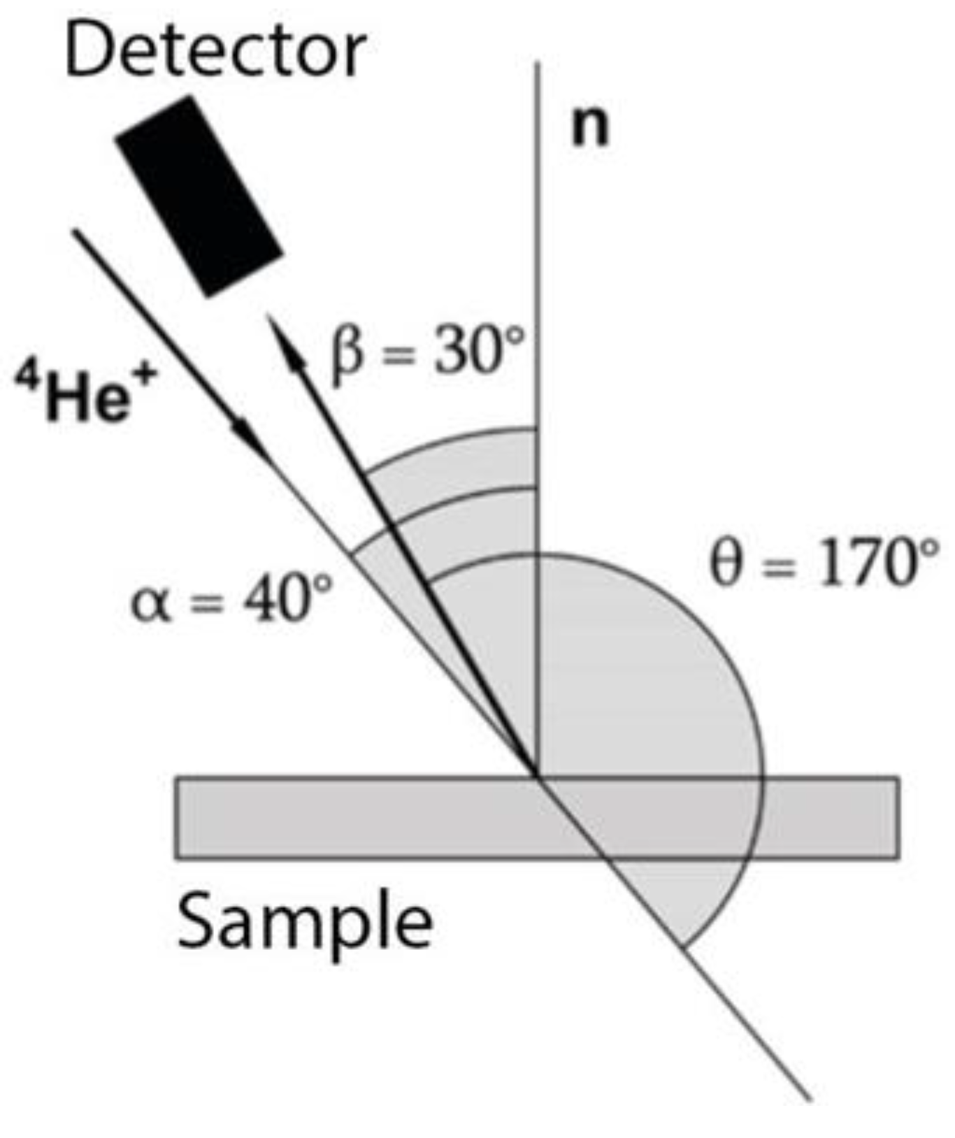
14]. The registration scheme for backscattered helium nuclei
4He
+ is shown in
Figure 1.
The figure shows the geometry of the detector location relative to the analyzing beam of helium ions and the studied Fe sample, the angles were equal to α = 40°, β = 30°, θ = 170°. For V and Ti samples, the angles were equal, respectively: for V, α = 10°, β = 0°, θ = 170°; for Ti, α = 0°, β = 10°, θ = 170°.
Angle α is the angle between the normal n to the sample and the direction of the incident beam; β is the angle between the normal n and the scattering direction at which the spectrum is taken; θ is the angle between the direction of the beam passing through the sample and the scattering direction (backscattering angle).
The H
2 distribution profile was measured using the Elastic Recoil Detection Analysis (ERDA). In this case, an Al foil was placed in front of the detector, the thickness of which was chosen so that the helium ions scattered by the nuclei of all elements at an angle of 30° were absorbed in it almost completely, and the recoil protons lost the minimum energy. Model calculations were used to determine the atomic concentration and the depth of occurrence of elements in samples of Fe, V, and Ti. To determine the depth of occurrence of elements, the values of the atomic densities of the chemical compounds Fe, V and Ti were used [
8]. The depth of occurrence of elements was calculated based on the average density of the layer using formula (1):
is the average density of the layer [at./cm
3], Ci is the atomic concentration of the element i in the layer (a fraction of 100%),
Pi is the atomic density of the element i [at./cm
3].
For hydrogen and oxygen, tabular Pi values were taken for gases in the molecular state.
3. Results
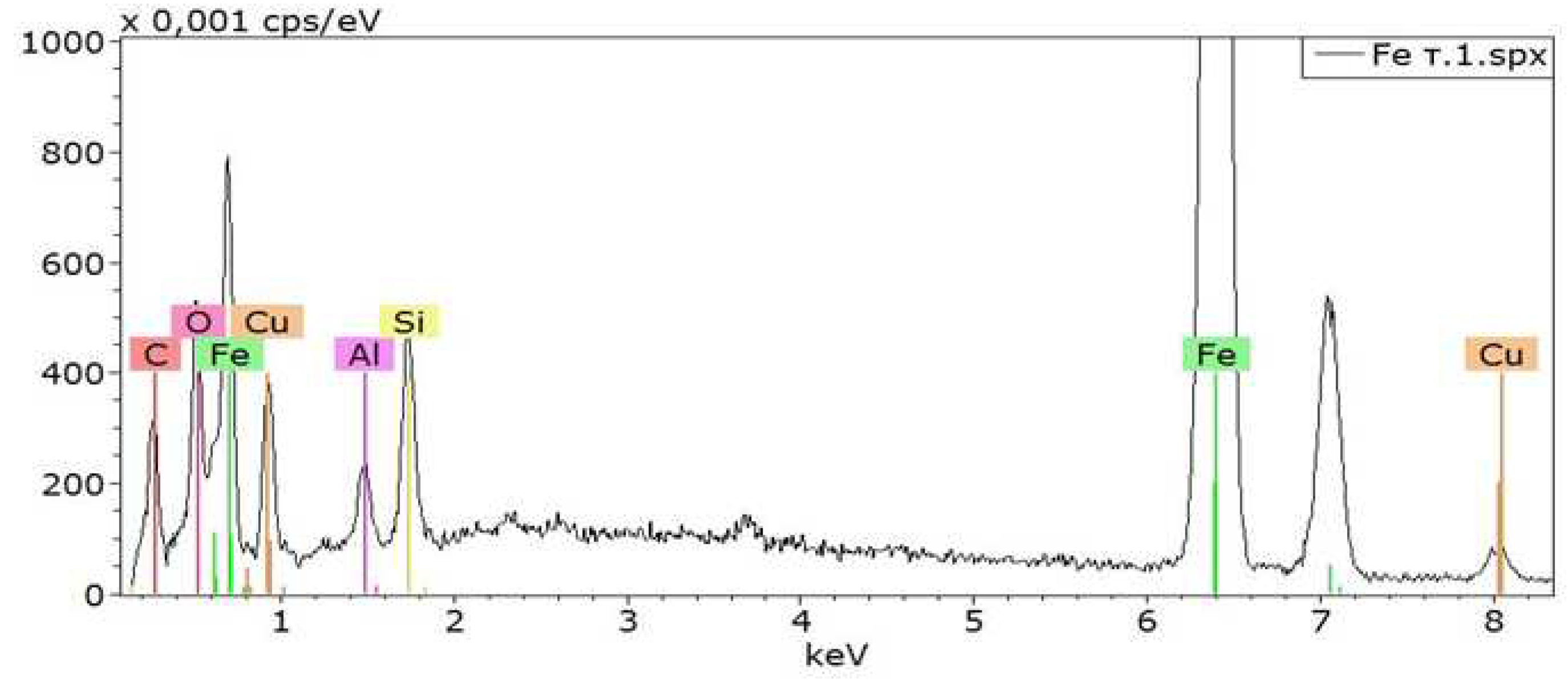
Figure 2 shows the spectrum of elements on the surface of the Fe sample when Cu is sprayed through a stainless steel tube. It can be seen that elements are observed on the Fe surface: copper (Cu), silicon (Si), aluminum (Al), carbon (C) and oxygen (O). Chemical elements – C, Si and Al come from the anode unit of the installation [
19].
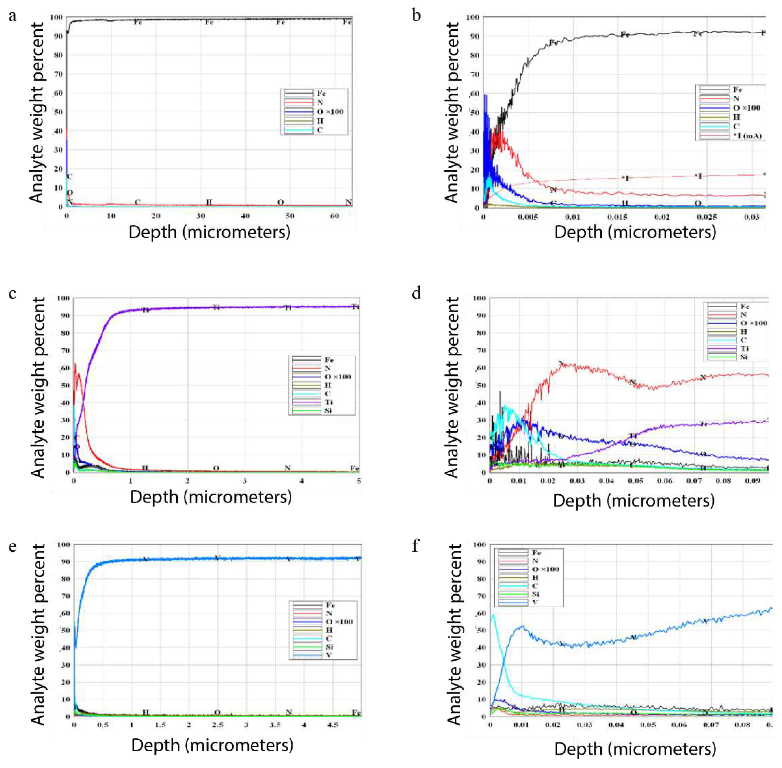
Figure 3 (a - f) shows the distribution profiles of elements in the initial samples – Fe, V and Ti, obtained by quantitative layer-by-layer analysis. Impurities are visible on the surface of the samples: C, O
2, H
2 and N
2, the main components of air and water. At depths of more than 5 nm, pure Fe, V and Ti are observed, as well as an insignificant concentration of Si. A transition layer is visible on all samples, the thickness of which depends on the density of the metal – 0.01 microns (Fe); 0.5 microns (V); 1.0 microns (Ti).
It can be seen that the surface of the initial metal samples contains large amounts of N
2 and C, while O
2 and H
2 are observed in lower concentrations. The presence of these elements is associated with the absorption of gases by the films: CO
2, N
2, and H
2O vapors from the atmosphere. Fe and Si particles get into the V and Ti samples during grinding on a glass plate and from a fixture made of steel. The penetration depth of impurities in Fe reaches ~60 µm (
Figure 3a); in V and Ti is ~5 µm (
Figure 3c, e). Parameter I* (
Figure 5b) is the plasma current in the glow discharge atomic emission spectrometer GDS 850A. Up to 0.005 microns, the current is stabilized and all indicators should not be taken into account.
On
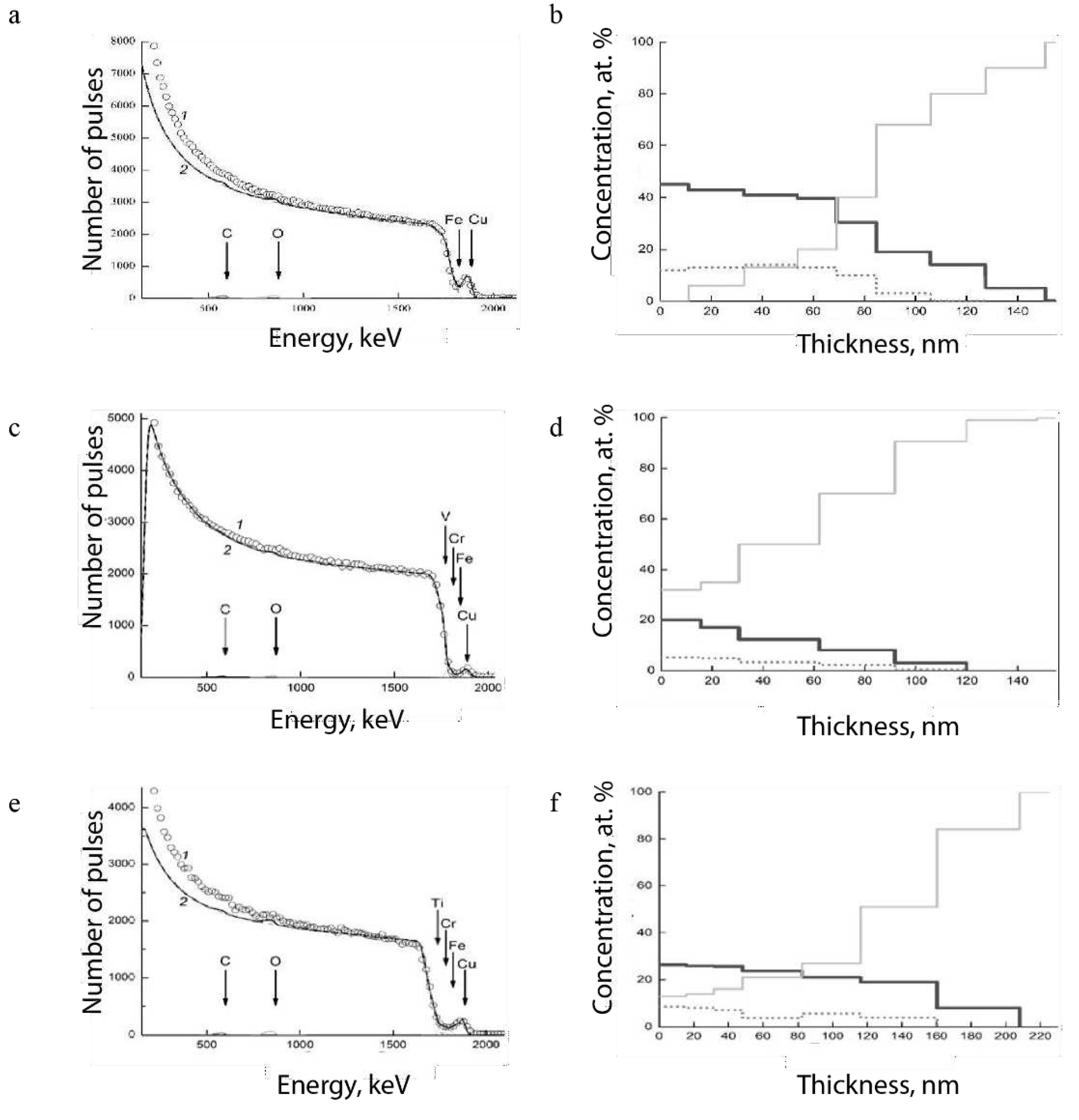
Figure 4 (a - c) shown the RBS spectra of the samples Fe, V, and Ti (experimental curve 1). The calculated spectra (curve 2), which are the sum of all partial spectra associated with the scattering of helium ions
4He
+ by the nuclei of the elements that make up the Cu films on the surface of the samples: Fe, V and Ti – C, O, Cr, and Fe [
20].
Figure 4.
Experimental (1) and calculated using the SIMNRA program (2) backscattering spectrum of 4He+ ions in Fe (a, b), V (c, d) and Ti (e, f) samples: carbon (C) – solid black line; copper (Cu) – dotted line; substrate material – Fe, V, and Ti – dash-dotted line.
Figure 4.
Experimental (1) and calculated using the SIMNRA program (2) backscattering spectrum of 4He+ ions in Fe (a, b), V (c, d) and Ti (e, f) samples: carbon (C) – solid black line; copper (Cu) – dotted line; substrate material – Fe, V, and Ti – dash-dotted line.
It should be noted that other chemical elements also affect the RBS spectrum (
Figure 2 and
Figure 3), but their influence is insignificant due to the low concentration. Note that Cu films were not studied in the work by layer-by-layer analysis on a GDS 850A atomic emission spectrometer, which was due to the need to have fairly uniform films ~20x20 mm
2 in size. It was not possible to obtain Cu films of such sizes using the Plasma Focus PF-4 setup. On
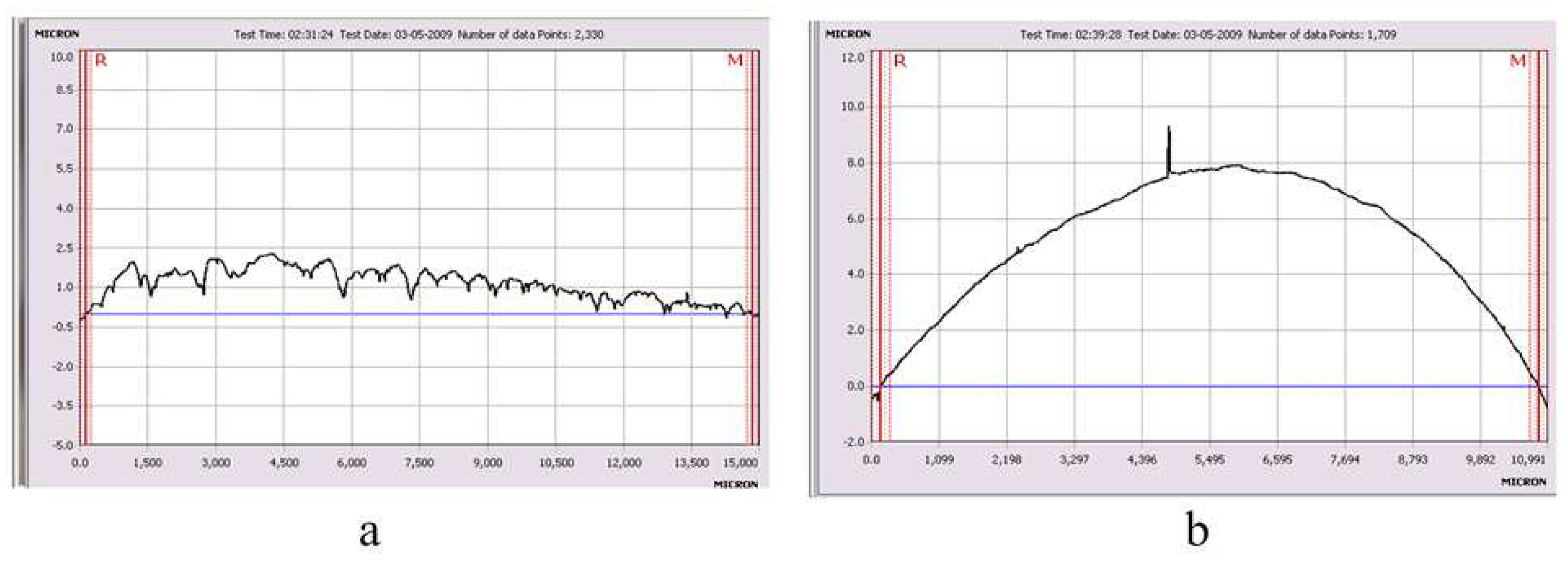
Figure 5 (a, b) shows the distribution profiles of Cu on the surface of metals: V and Fe.
Figure 5.
Copper film profile on (a) V sample and (b) Fe sample.
Figure 5.
Copper film profile on (a) V sample and (b) Fe sample.
Copper films on sample V have a thickness in the range of 0.5-2.5 µm. In the case of Fe and Ti samples, it was not possible to determine the film thickness due to the insufficient planarity of the samples. In this case, the profilometer scans the profile of the sample surface, against which it is almost impossible to determine the thickness of the copper film (
Figure 5b).
4. Discussion
From the results (Figure 4) it follows that the penetration depth of C atoms in Fe is ~150, V ~120 and Ti ~210 nm. The depth of occurrence of Cu atoms depends on the density of the metal: Fe (7.86 g/cm
3) ~105, V (6.11 g/cm
3) ~120 and Ti (4.51 g/cm
3) ~160 nm. The large depth of occurrence of Cu in Ti is associated with a lower density of the metal and its oxides in comparison with Fe and V. These considerations are confirmed by data on the density of the main metal oxides: Fe
2O
3 – 5.24 g/cm
3, V
2O
3 – 4.87 g/cm
3 and TiO
2 – 4.25 g/cm
3 [
21]. The initial samples of Fe, V and Ti metals in thin surface layers of ~5-10 nm contain about several weight percent of various impurities: C, O
2, H
2, N
2 and others. The depth of occurrence of these impurities in Fe can reach 60 µm (
Figure 3a). In vanadium and titanium, the depth of occurrence is about 5 µm (
Figure 3c, e).
Thus, Cu particles, penetrating to a depth of about 100-150 nm, are in a metal layer with a sufficiently high level of doping with various impurities. This metal layer will have a significant effect on the electrical and mechanical properties of Cu films. In addition, Cu films have an inhomogeneous structure, as indicated by the scanning profile (
Figure 5a). Given that microelectronics uses conductive tracks with a thickness of the order of several hundred nanometers or less, one can expect Cu to penetrate the entire thickness of the material, which should ensure good adhesion with conductors made of refractory materials and their sufficiently high electrical conductivity.
5. Conclusions
The profiles and concentrations of the elements: C, O2, N2, and H2 on the surface of the initial metal samples: Fe, V, and Ti were determined by layer-by-layer quantitative analysis on a GDS 850A glow-discharge atomic emission spectrometer. It is shown that a "loose" transition layer with a thickness of ~1 μm exists on the surface of metals in the initial state. Rutherford backscattering of 4He+ ions with an energy of 2.451 MeV was used to determine the depth and distribution profile of Cu and C atoms under the surface of Fe, V, and Ti metals. The penetration depth of Cu particles in Fe is ~100 nm; V ~120 nm; Ti ~160 nm. It is assumed that the physical properties of the transition layer ~1 μm thick in metals: Fe, V, and Ti will determine the properties of Cu films (adhesion, electrical resistance, etc.). Using an AMBIOS XP-200 type profilometer, the thickness of the Cu film on the metal surface was determined to be ~0.5–2.5 µm.
Funding
The study was performed in the scope of the Russian Federation state order No. 075- 00715-22-00 and 0023-2022-0004, H2020/MSCA/RISE/SSHARE number 871284 project, RO-JINR project No. 366/2021 item 84, Serbia—JINR cooperation Projects No. 178 2021 items 7 and 8, Vietnam—the International Center of Physics at the Institute of Physics Grant ICP.2022.04.
Acknowledgments
The authors are grateful to Ph.D. I.V. Borovitskaya for help in preparing metal samples and Ph.D. A.I. Gaidar for measuring the spectra of elements.
References
- Chen, T.; Liu, Y. Semiconductor nanocrystals and metal nanoparticles: Physical Properties and Device Applications. In Advances in Materials Science and Engineering; CRC Press: Boca Raton, 2017. [Google Scholar] [CrossRef]
- Kalita, V.I.; Komlev, D.I. Plasma coatings with nanocrystalline and amorphous structures, Lider M, Moscow, 2008.
- Shmakov, M.; Parshin, V. Hybrid-film integrated circuits: The choice of materials and what to consider when designing. Technologies in the Electronic Industry 2007, 2, 64–70. [Google Scholar]
- Einspruck, N.; Brown, D. Plasma technology in the production of VLSI, MIR, Moscow, 1987.
- Lyubchyk, A.; Filonovich, S.A.; Mateus, T.; Mendes, M.J.; Vicente, A.; Leitão, J.P.; Falcão, B.P.; Fortunato, E.; Águas, H.; Martins, R. Nanocrystalline thin film silicon solar cells: A deeper look into p/i interface formation. Thin Solid Films 2015, 591, 25–31. [Google Scholar] [CrossRef]
- Makarova, T.L.; Zakharchuk, I.; Geydt, P.; Lahderanta, E.; Komlev, A.A.; Zyrianova, A.A.; Lyubchyk, A.; Kanygin, M.A.; Sedelnikova, O.V.; Kurenya, A.G.; Bulusheva, L.G.; Okotrub, A.V. Assessing carbon nanotube arrangement in polystyrene matrix by magnetic susceptibility measurements. Carbon N Y. 2016, 96, 1077–1083. [Google Scholar] [CrossRef]
- Saltykov, S.N.; Hoviv, A.M. , Interpenetration of iron and copper in thin films and their phase composition during sequential deposition. Condensed Media and Interphase Boundaries 2010, 12, 61–65. [Google Scholar]
- Sedneva, T.A; Lokshin, E.P.; Belikov, M.L.; Belyaevsky, A.T. Synthesis and properties of composites based on oxides of titanium (IV), copper (II) and sodium (I). Inorganic Materials 2014, 50, 1195–1204. [Google Scholar] [CrossRef]
- Tikhonov, A.A.; Filippov, D.A.; Manicheva, I.N. Method for manufacturing magnetoelectric structures, № RU 2682504, 2019.
- Meyer, J. Ion implantation in semiconductors: silicon and germanium; Academic Press: New York, 2012. [Google Scholar]
- Petrov, E.G.; Shevchenko, Y.V.; Gorbach, V.V.; Lyubchik, S.B.; Lyubchik, A.I. Features of gate-tunable and photon-field-controlled optoelectronic processes in a molecular junction: Application to a ZnPc-based transistor. AIP Adv. 2022, 12, 105020. [Google Scholar] [CrossRef]
- Petrov, E.G.; Gorbach, V.V.; Ragulya, A.V.; Lyubchik, A.; Lyubchik, S. Gate-tunable electroluminescence in Aviram–Ratner-type molecules: Kinetic description. J Chem Phys. 2020, 153, 084105. [Google Scholar] [CrossRef] [PubMed]
- Borynyak, L.; Nepochatov, Yu. Investigation of increasing adhesion of multilayer metallization coatings to dielectric substrates of hybrid integrated circuits. Technologies in the Electronic Industry 2007, 5, 67–71. [Google Scholar]
- Klimachev, I.I. Fundamentals of technology and design of GIS microwave range, Technosfera, Moscow, 2006.
- Kolokoltsev, V.N.; Kulikauskas, V.S.; Bondarenko, G.G.; Eriskin, A.A.; Nikulin, V.Ya.; Silin, P.V. Determination of the element distribution in films deposited using the plasma focus facility by Rutherford backscattering. Surface X-Ray Synchrotron and Neutron Studies 2017, 11, 63–68. [Google Scholar] [CrossRef]
- Eliseev, S.P.; Nikulin, V.Ya.; Oginov, A.V.; Tikhomirov, A.A. ; Plasma diagnostics in the optical and X-ray regions on the plasma focus device PF-4 (installation Tyulpan). Problems of Atomic Science and Technology. Series: Plasma Physics 2006, 12, 147–149. [Google Scholar]
- Kobzev, A.P. Elemental Analysis of Nanostructures on Charged Particle Beams. In Nuclear Physics and Nanotechnologies. Nuclear-Physical Aspects of the Formation, Study and Application of Nanostructures; Sisakyan, A.N., Ed.; JINR: Dubna, 2008; JINR: Dubna, 2008; pp. 142–154. [Google Scholar]
- Feldman, L.; Mayer, J. Fundamentals of surface and thin films analysis; North-Holland: Monograph, New York, 1986. [Google Scholar]
- Kolokoltsev, V.N.; Borovitskaya, I.V.; Nikulin, V.Ya.; Eriskin, A.A.; Silin, P.V.; Kalita, V.I.; Komlev, D.I. On the content of impurities in films deposited on Plasma focus devices. In Proceedings of the VI International Conference with Elements of a Scientific School for Youth “Functional Nanomaterials and High-Purity Substances”, Suzdal, Moscow; 2016; pp. 247–248. [Google Scholar]
- Mayer, M. «SIMNRAUsersGuide», (n.d.). Available online: http://portal.if.usp.br/lamfi/sites/portal.if.usp.br.ifusp/files/simnra.pdf (accessed on 7 March 2023).
- Kazenas, E.K.; Tsvetkov, Yu.V. Evaporation of oxides, Nauka, Moscow, 1997.
|
Disclaimer/Publisher’s Note: The statements, opinions and data contained in all publications are solely those of the individual author(s) and contributor(s) and not of MDPI and/or the editor(s). MDPI and/or the editor(s) disclaim responsibility for any injury to people or property resulting from any ideas, methods, instructions or products referred to in the content. |
© 2023 by the authors. Licensee MDPI, Basel, Switzerland. This article is an open access article distributed under the terms and conditions of the Creative Commons Attribution (CC BY) license (http://creativecommons.org/licenses/by/4.0/).
