1. Introduction
In the present era, achieving low power consumption has become a paramount requirement in design of integrated circuits (ICs) and complex system-on-chip (SoC) configurations. Contemporary advancements and research in the realm of portable electronic devices predominantly concentrate on design principles towards energy savings, operation under reduced voltage conditions, and integration of different mixed-signal circuits and/or systems into a singe monolithic chip. Generally, analog circuits tend to be the most power-hungry subsystems within SoCs. As a result, in the majority of instances, having knowledge regarding the specific load or current consumption can provide an efficient method for lowering the power dissipation of the entire system. Furthermore, advances in IC manufacturing are welcome but leads to sophisticated technologies with notable deviations in process characteristics. As a consequence, ensuring the IC performance with resilience to process-voltage-temperature (PVT) variations becomes one of the most demanding endeavors for both IC designers and researchers. This concern becomes particularly critical when addressing circuits requiring a high degree of precision.
The established measure of electric current coursing through a specific circuit could be highly advantageous in controlling other components within a system. An example of a system, where electric current can be used as a control signal is controller in DC-DC converters. A flyback DC-DC converter is categorized as a straightforward configuration of an isolated converter, extensively employed as the power supply circuit in cellphones, laptops, PCs, LCD TVs, and various other portable gadgets [
1].
Within on-chip current sensing techniques, the typical approach involves a direct method of current measurement utilizing a sensing element. This often includes components like a shunt resistor, a MOS transistor configured as a resistor, or a sensing transistor connected in parallel with the power MOS device [
2,
3,
4,
5,
6,
7]. The main properties and features of such techniques are described in more detail in [
4]. However, the main disadvantages of direct measurement approaches include low accuracy and rather high power losses across the sensing element. Conversely, indirect methodologies provide the opportunity to detect current without requiring an extra sensing element connected in series. In this way, they present lossless options for on-chip measurement of electric current. These techniques leverage alternative electrical parameters that are directly correlated with the sensed current. Thus, indirect methods do not influence performance of a measured circuit through additional measurement hardware.
In this paper, we present the slope detector circuit designed in 65nm CMOS technology, which can be used for indirect on-chip current measurement and then, controlling the flyback DC-DC converter.
Section 2 elaborates on the fundamental concept underpinning the devised slope detector. The simulation-derived outcomes are displayed in
Section 3, while the actual measured results are exhibited in
Section 4. The utilization of the indirect measurement approach is outlined in
Section 5, and the paper culminates with the drawn conclusions in
Section 6.
2. Background and Motivation
As mentioned above, many portable electronic devices use Flyback DC-DC coverter as a power source due to its electrical isolation and simple topology. Under light-load conditions or standby mode, Flyback converter usually works in so-called “burst” mode [
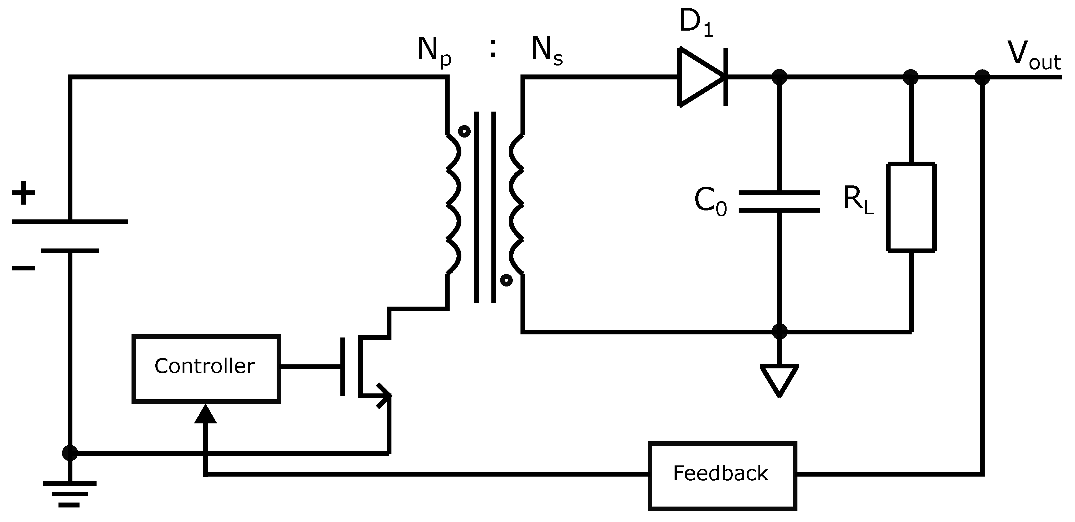
8]. In order to regulate the converter output voltage and control the voltage ripple, the output current and voltage of converter need to be estimated. For this purpose, direct sensing approaches using auxiliary winding of the transformer are usually employed. However, the typical Flyback converter topology includes an output bypass capacitor to reduce voltage ripple at the converter output. The output current can therefore, be estimated indirectly just by sensing a voltage drop across the capacitor. This is the main idea behind such an indirect method of measuring the output current of Flyback DC-DC converter working in the burst mode. The basic topology of Flyback converter and typical waveform of the signals are shown in
Figure 1 and
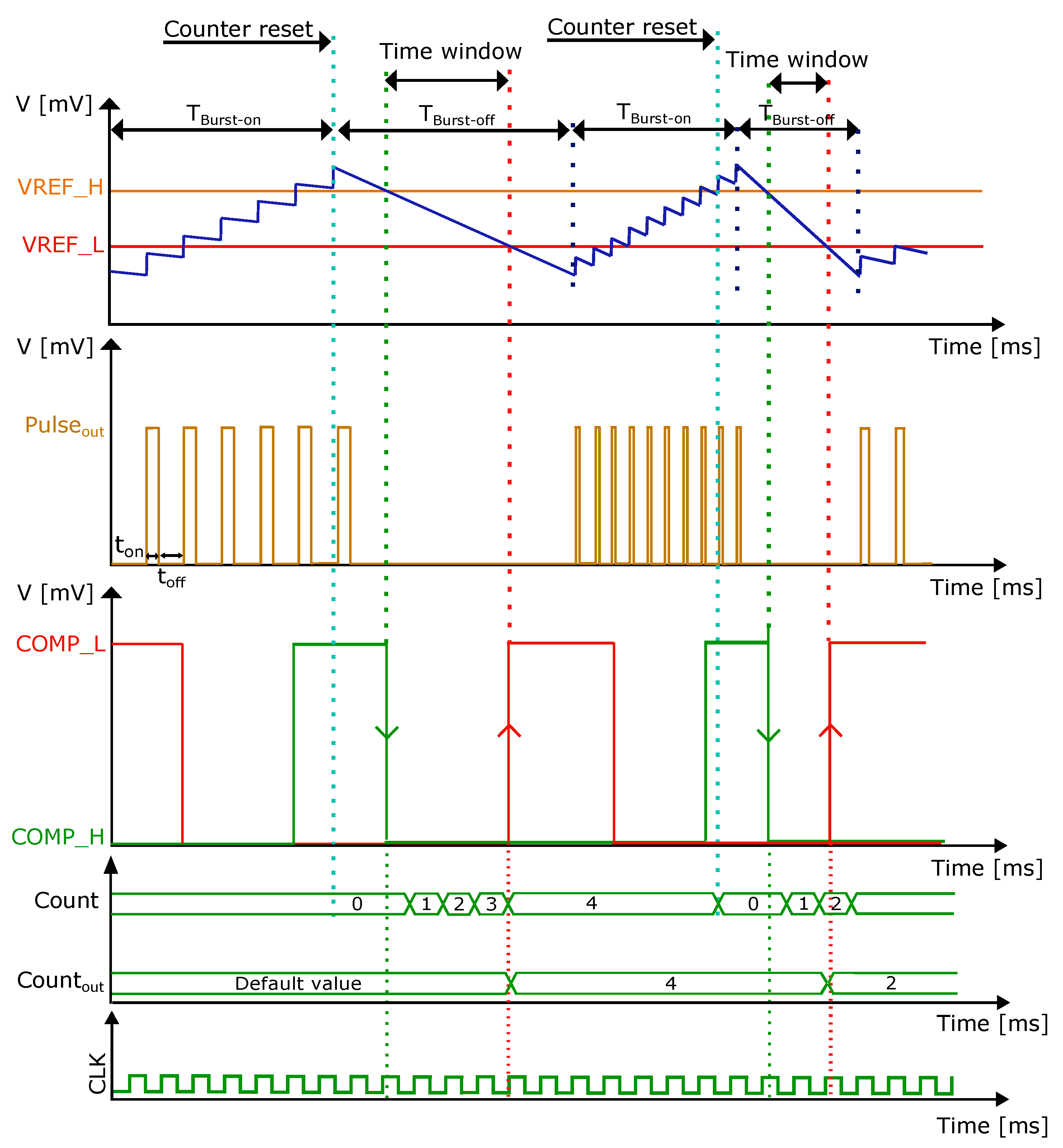
Figure 2, respectively. It can be observed that the burst mode contains two phases: burst-on and burst-off periods. During the burst-on time, the output voltage is boosted to the requested value. On the other hand, during the burst-off time, the converter output voltage decreases due to current flow from the output capacitor to the load. Hence, the output current of converter can be sensed during this phase indirectly by sensing the output voltage. The proposed sensing approach presented in this paper is based on the idea described above.
This operational concept outlines the fundamental operation of the BUCK-BOOST converter. When the power transistor switch is turned on, it collects energy from the power source and stores it within the primary winding of the transformer. Subsequently, while the transistor is turned off, the stored energy is transferred to the secondary winding of the transformer and eventually delivered as the output voltage by the converter [
9,
10]. Enhancing the energy conversion efficiency of the converter can be achieved by sensing the load current and strategic control of the power MOS switch, which is performed by the controller (see
Figure 1). Thus, it is rather evident that the output current sensing needs to be performed within the integrated circuit of DC-DC converter [
11,
12,
13].
The waveforms depicted in
Figure 2 illustrate the signal sequence in context of the implemented current measurement approach. The diagram displays the following signals (waveforms from top to bottom): DC-DC flyback converter output voltage (blue curve), the input references such as VREF_H and VREF_L (orange and red curves), the outcome from the pulse generator responsible for driving the power transistor switch, outputs from comparators COMP_L and COMP_H, the actual state of the counter denoted as
(an internal signal), the output stemming from the measurement method referred to as
, and finally, the CLK signal. Following the global reset activation,
value returns to its default value, which in turn configures the default waveform of
. As the converter output becomes charged, it ascends until it reaches the predefined upper voltage limit (VREF_H). Amid the discharge phase, the measurement process is initiated. With each rising edge of the clock signal, the value of
is incremented. Once the designated measurement time window has elapsed, the value of
is written to the output register
. This value is then utilized to select the appropriate waveform for the
signal from a Look-Up Table. Upon the VREF_H threshold being achieved by the output signal, a counter reset is triggered, returning the internal counter value to zero.
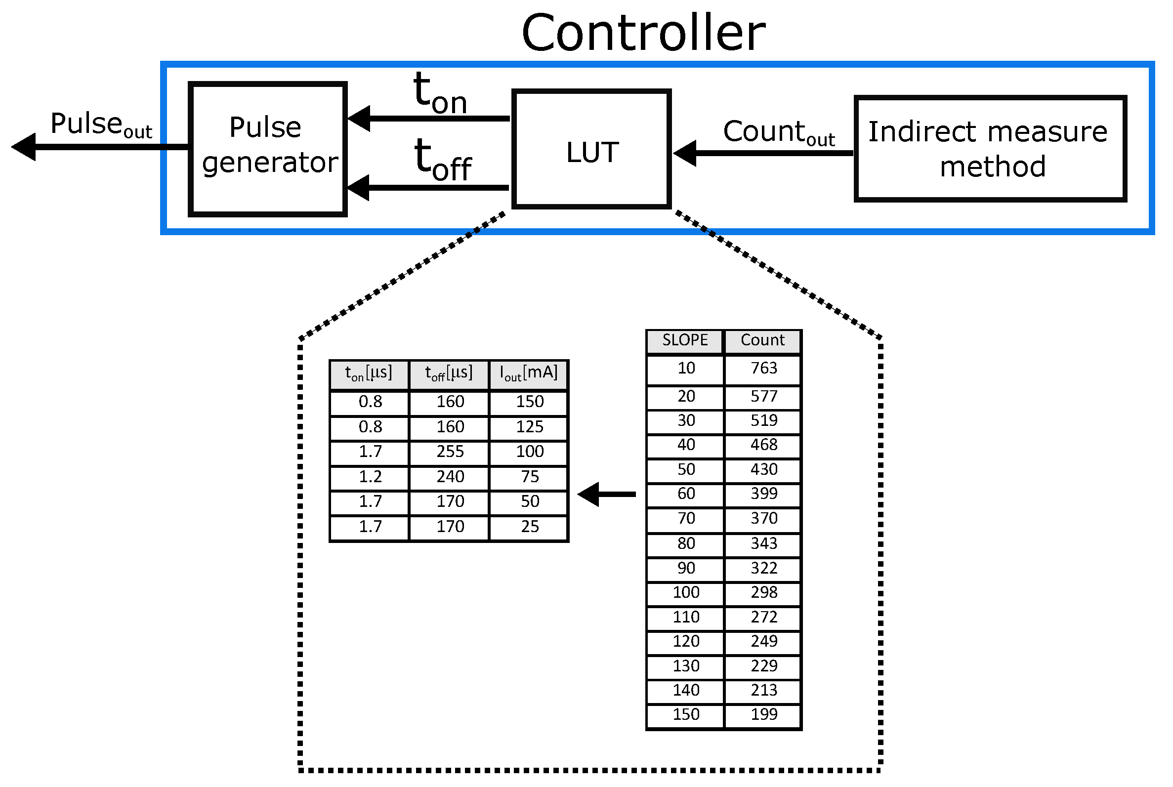
As introduced earlier, the proposed load current measurement technique relies on an indirect approach involving voltage drop sensed across the external capacitor on the DC-DC flyback converter output. The designed measurement system was implemented though a controller circuit to ensure the controlled switching of the power NMOS transistor on the primary side of transformer. The comprehensive block diagram of the developed controller is illustrated in
Figure 3. The controller consists of three main components: the proposed indirect measurement method of the output current, a lookup table (LUT), and a pulse generator. The pulse generator is a sequential circuit that was described at the RTL (Register Transfer Level) using Verilog language. It generates the control signal named
, which drives the power NMOS switch. The control signal is determined by the input parameters
and
. The input signals for the pulse generator are fed from the LUT block that can be programmed externally using a digital logic. An instance of LUT configurations is shown in
Figure 3, where the left-side table (within the LUT) illustrates configuration of the parameters
and
based on the measured current value. These values were obtained by simulation, and with these parameters, the converter achieved optimum efficiency. The right-side table presents the conversion table that correlates the finite counter values with the corresponding currents. The input applied to the LUT, which is a 10-bit value, is obtained by the designed current measurement method.
3. Proposed Slope Detector Circuit
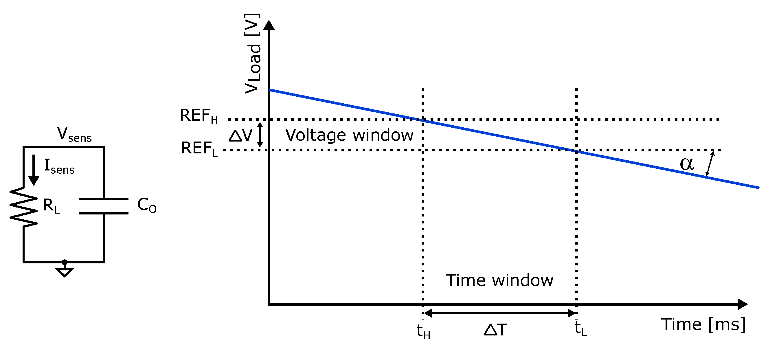
Basic principle of the proposed slope detector (SD) circuit is depicted in
Figure 4. Since the designed SD is intended to be used in the presented controller for DC-DC converter, the output voltage representing the output load current can be sensed through the external capacitor (converting the output load current to voltage value). This approach is based on an assumption of using a large bypass capacitor that is an existing component of the converter. In such a case, during the discharging phase of capacitor
, the output voltage will vary linearly in time. The sensed load current
can be expressed as follows:
where
is the output voltage,
is the load resistor and
is the output capacitor (see
Figure 1). The output voltage will vary linearly in time if we considered that
. This condition is ensured only if either the current sensing is carried out in a short time interval or the capacitor discharging time constant
will be large. Thus, if one of these two conditions is fulfilled, the electric current can be conveniently sensed in the indirect manner by measuring the slope of voltage across the capacitor
within its discharging phase.
The measured time window is given by two voltage reference
and
(denoted as the voltage window
in
Figure 4). In such a case, the respective electric current will be given as:
It is important to note that accuracy of the proposed current measurement approach can be influenced by process, temperature and supply voltage variations. Such fluctuations are not considered in Equation (5) but these will be further investigated in the following part of the paper.
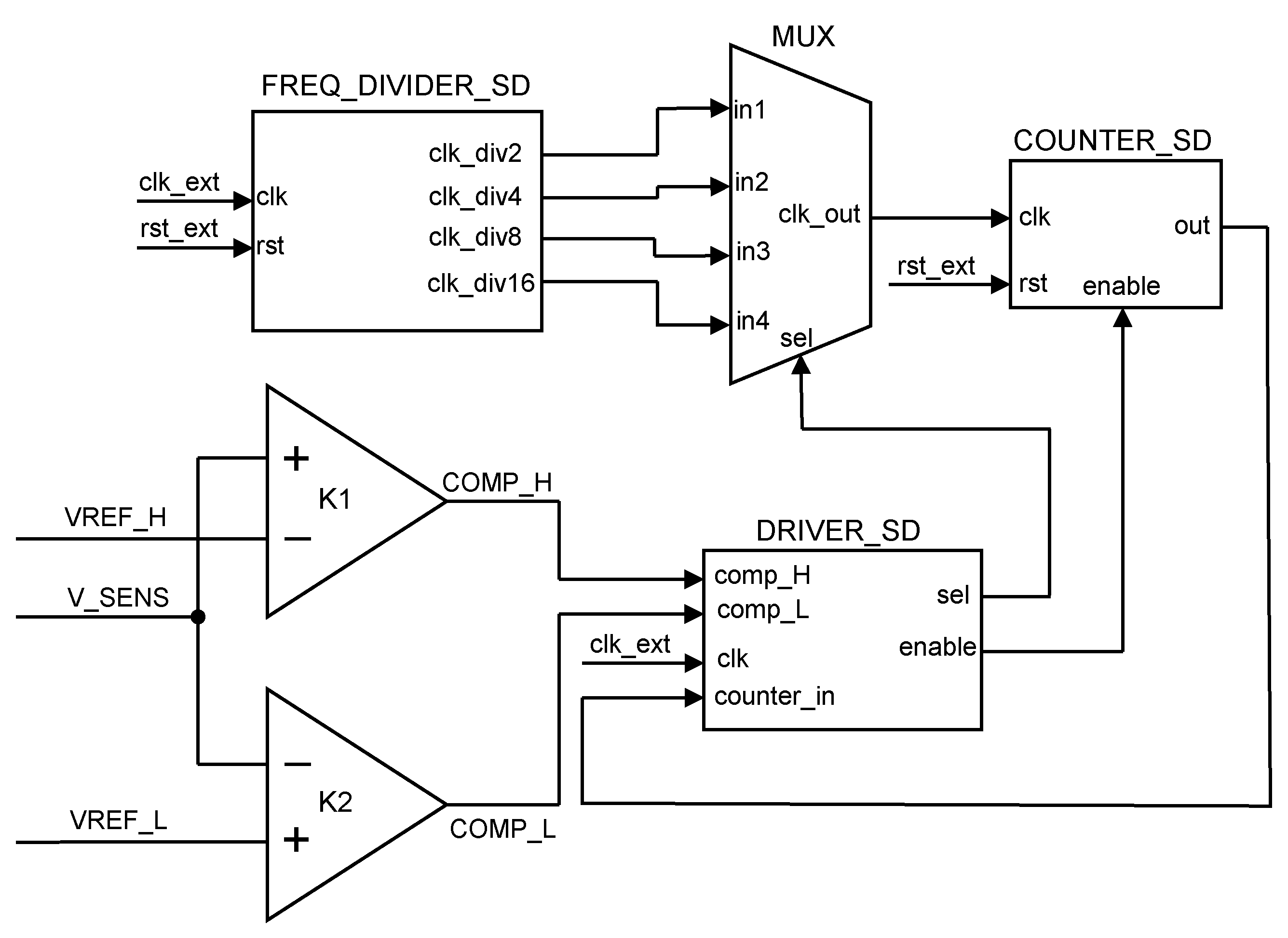
The circuit block diagram of the designed slope detector is depicted in
Figure 5. The output voltage denoted as
across the capacitor
is sensed by a window comparator (forming by comparators K1 and K2). Both comparators are based on a common topology with hysteresis introduced to protect the circuit from unwanted glitches at the comparator output. Digital outputs of comparators K1 and K2 control the start/stop switching of the counter, which is driven by
signal with frequency of 500 kHz (considering the external input frequency of 1 MHz and multiplexer output being transferred from input
). In order to extend the range of possible slope that can be detected, the input frequency is decreased and multiplexed to the input of counter. This simple feature brings possibility of sensing a wider range of currents but on the other hand decreasing switching frequency of counter reduce accuracy of measurement system. After the counter stops counting, its value can be easily compared to the reference value stored in a Look-Up-Table (LUT), and the measured current is evaluated.
The slope value of the output sensed voltage ranges from 10 to 150, and the counter switching frequencies are set to 500 KHz, 250 KHz, 125 KHz, and 62.5 KHz. The achieved calculated results represent the ideal finite counter value without any measurement errors considered. These calculation results, obtained using Equations (
3) and (
4), are shown in
Table 1. In calculations, we take into account the specified time window length
, the change in output voltage
(set to 60 mV), and the counter switching frequency
.
Due to the window comparator circuit being employed to sense the voltage at capacitor
, the detection can be sensitive to process variations, including the input offset voltage of comparators. As a result, the delay of both comparators might influence the overall accuracy of proposed measurement method. For this reason, Equation (5) needs to be extended as follows:
where
and
is difference of the input offset voltage and transition delay of comparators (K1 and K2), respectively. In the proposed SD circuit, differences in the parameters will be mainly influenced by mismatch of devices forming the comparators. This mismatch caused by variations in manufacturing process, can lead to discrepancies in the performance of individual components. As a result, the input offset voltage and delay of the comparators can vary, affecting the accuracy and reliability of the measurement method.
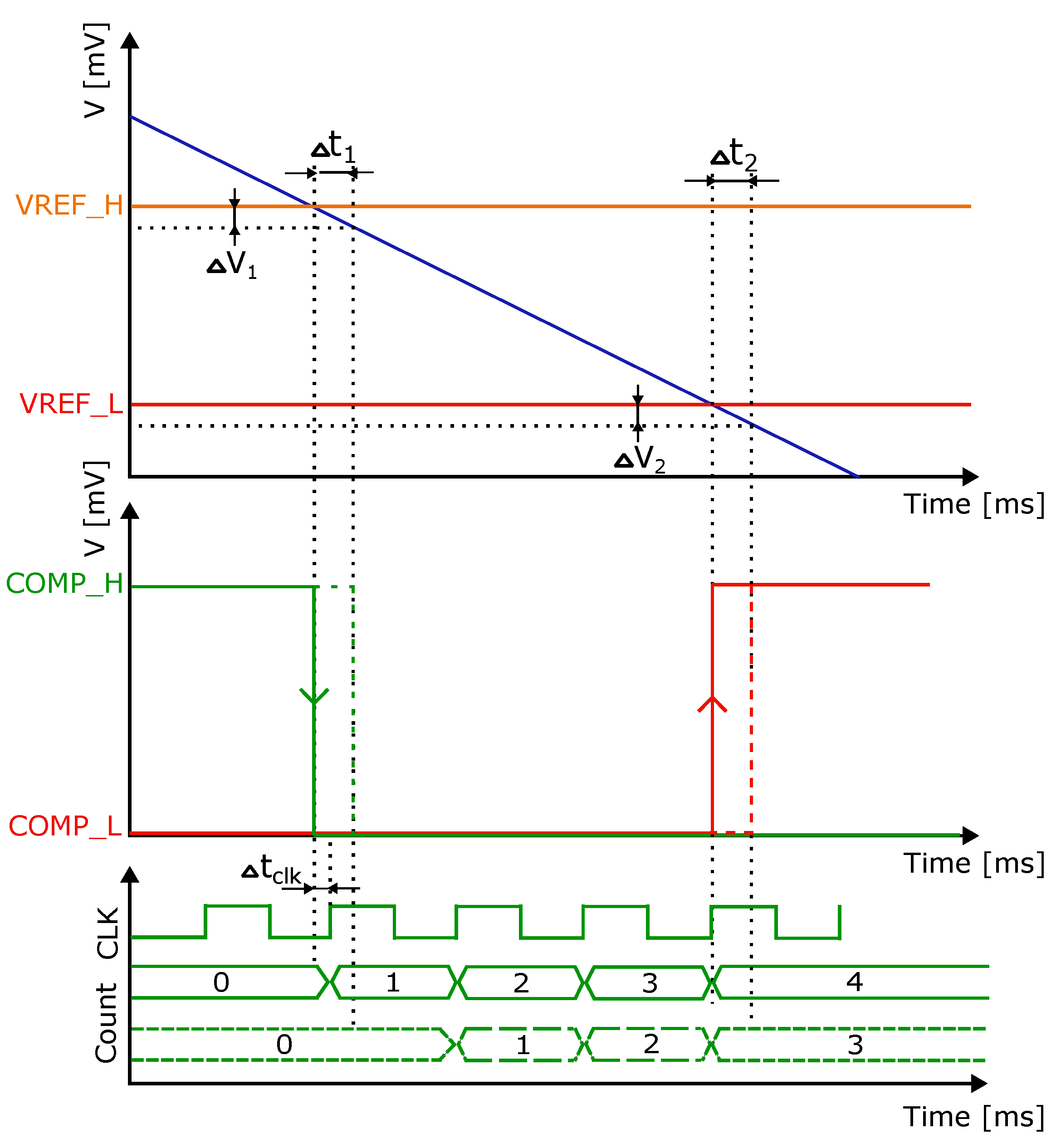
The waveforms shown in
Figure 6 illustrate the sequence of signals in measurement system (from top to bottom): comparator reference voltage inputs (VREF_H and VREF_L), outputs of the window comparator circuit (COMP_H and COMP_L), and finally, clock signal (CLK) and the counter output (Count). The counter output is set to zero by the external global reset and then, its value is incremented by each rising edge of the clock signal CLK. The middle graph displays the comparator outputs (K1 indicated by green color and K2 indicated by red) using continuous lines, without considering hysteresis and transition delays. Because the comparator circuits work asynchronously and their outputs are not synchronized with the clock signal, an error denoted as
might occur. In this scenario, the maximum delay error between the initial rising edge of the clock signal within the measurement window and the falling edge of comparator K1 output COMP_H may be less than one clock period. Likewise, a comparable measurement error can occur at the end of the measurement time window due to the lack of synchronization between the rising edge of comparator K2 output COMP_L and the rising edge of the clock signal. The hysteresis of comparators K1 and K2, denoted as
and
, respectively, and both comparators share the same hysteresis value. As a result of this hysteresis effect, delays named
and
will be present in the output signals of comparators K1 and K2, respectively. The comparator outputs and the counter values, with their delays, are depicted using dashed lines in middle and bottom graphs, respectively. The variances between
of comparator K1 and
of comparator K2 are consistently kept within a nanosecond range, even across different process corners. This slight difference is considered acceptable as it does not significantly affect the measurement time window.
4. Simulation Results
This section presents results obtained from simulation of the proposed slope detector circuit. The simulations took into account variations caused by fabrication process, and the designed circuit was analyzed using Corner and Monte Carlo (MC) analyses. The temperature range considered in all simulations was from C to C.
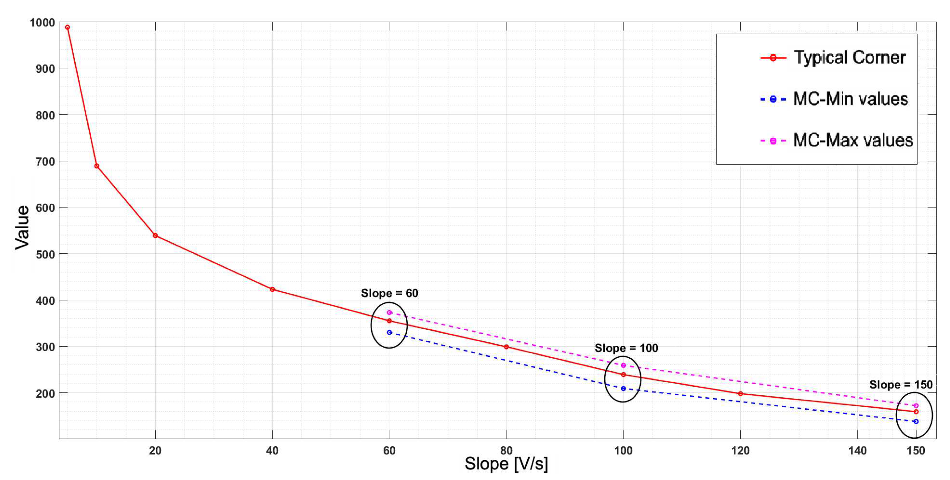
The relationship between the counter finite value and the sensed voltage slope is shown in
Figure 7. These results were obtained from both Corner Analysis and Monte Carlo. As the proposed slope detector operates by counting clock pulses within a specific time window, it exhibits robustness against variations caused by fabrication process fluctuation. The concept is primarily sensitive to any mismatch between the devices forming comparators K1 and K2.
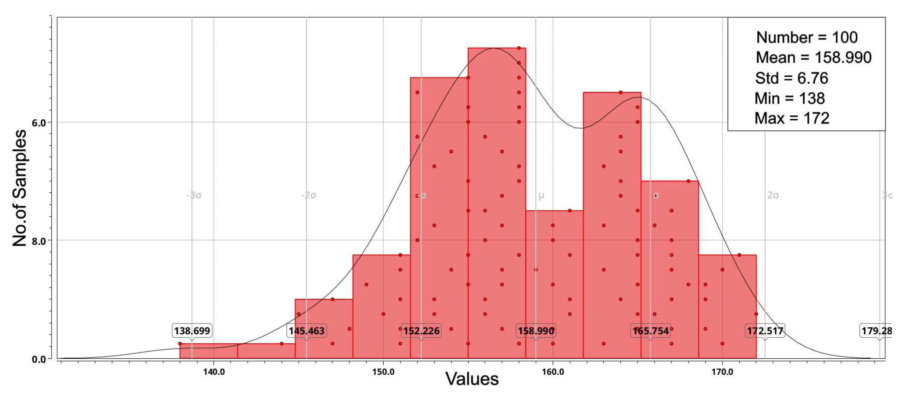
Results shown in
Figure 7 and
Figure 8 indicate that device mismatch introduces variations in the finite counter value, with a standard deviation of ±6 pulses counted by the counter. Counting for
variations, the accounted pulses can range from 138 to 172, with a mean value of 159. This parameter represents the overall error of the proposed approach, considering the mismatch of all devices used in the slope detector circuit.
The second part of the measurement error is caused by
(see
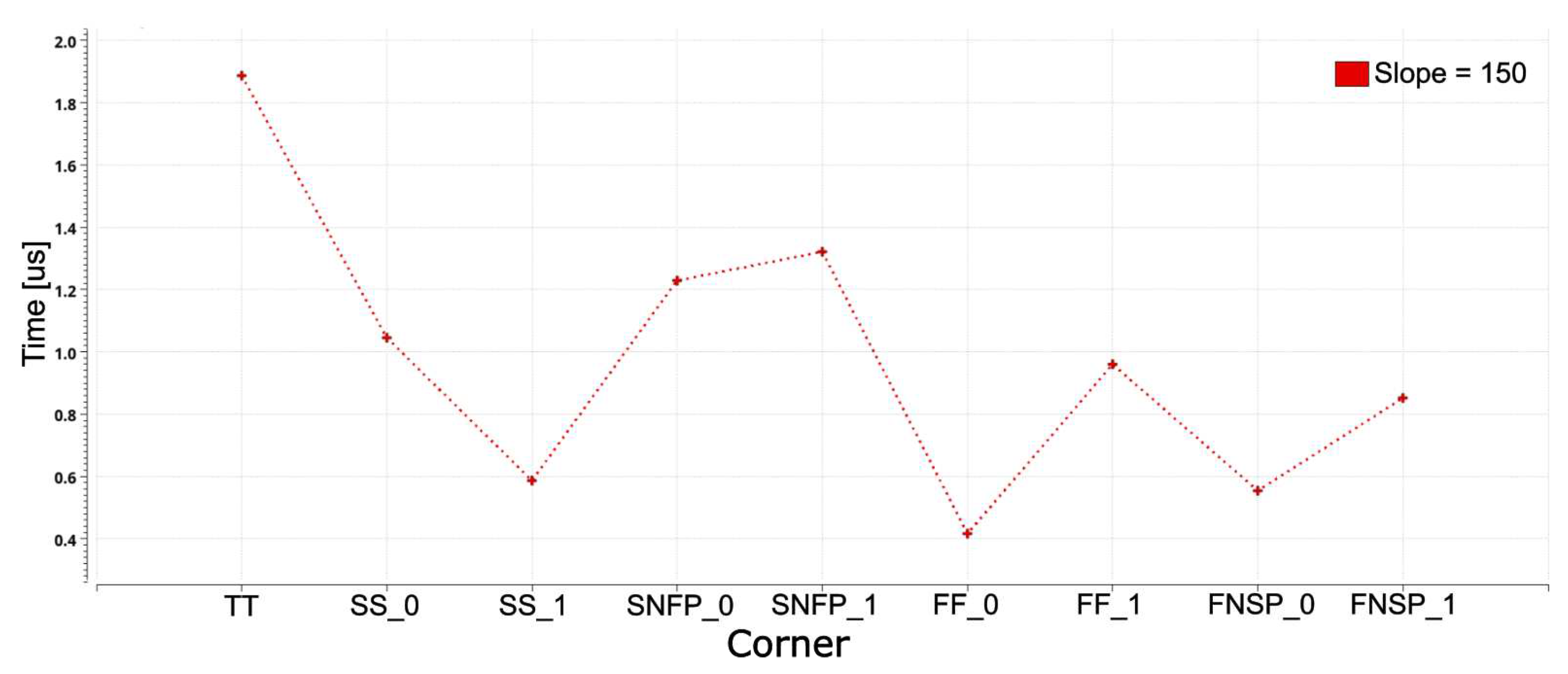
Figure 6) and explained in the previous section. In
Figure 9,
error over the process corners for slope of 150 V/s is shown. It can be observed that
can exhibit variations across different process corners, leading to a measurement error of approximately 2
. For the input frequency of 1 MHz, this implies that in a process corner,
can have an undesirable impact on the finite counter value, resulting in the addition of 1 to 2 extra pulses counted by the counter. It is essential to highlight that
was examined for various slope values, and in most cases, the maximum measurement error of 2
was observed.
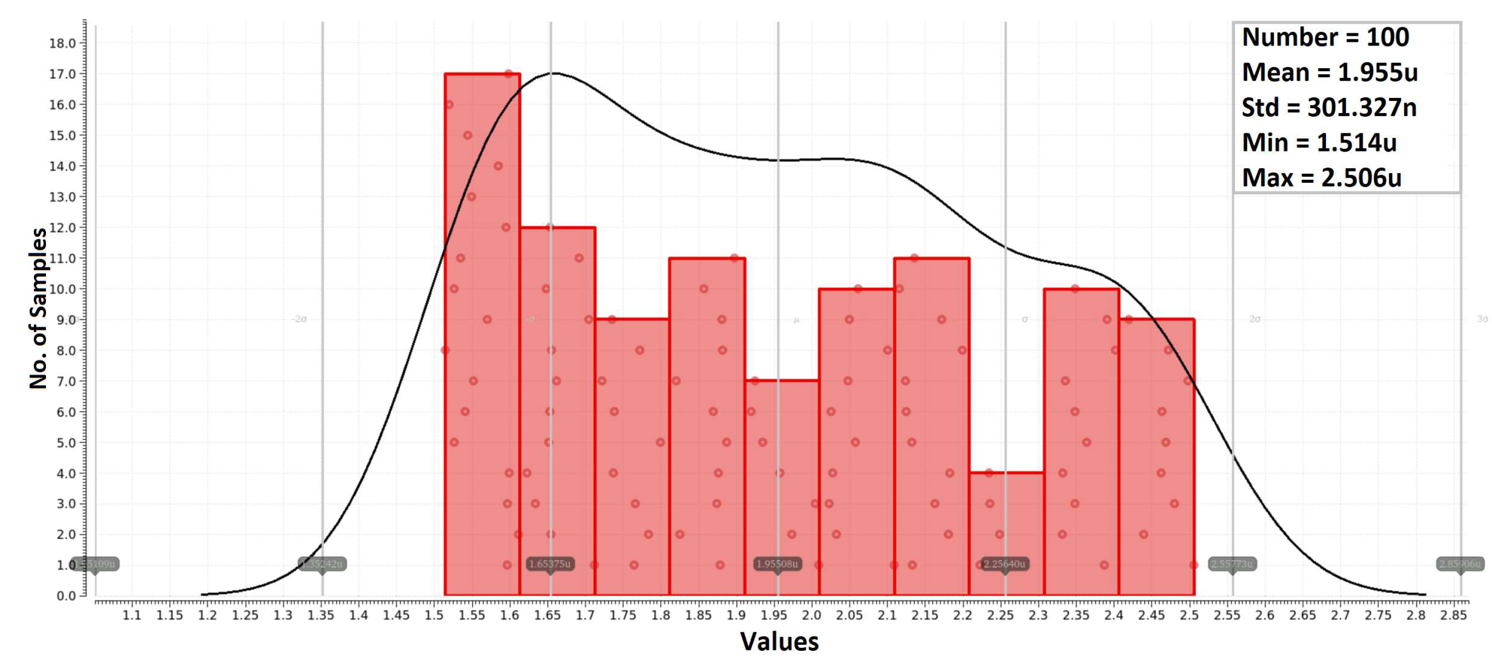
Figure 10 illustrates the results of Monte Carlo analysis for the
error at a slope of 150 V/s. Considering variations of
, the value of
can vary within the range from 1.512
to 2.506
, with a mean value of 1.955
s.
The maximum current error caused by the
effect was determined using Equations (
6) and (
7). In these equations,
represents the calculated current error,
is the value of the external capacitor,
denotes the change in the sensed output voltage,
is the duration of the time window, and
represents the maximum error caused by the asynchronous operation of comparators K1 and K2. If the counter switching frequency remains constant during the measurement process,
can be calculated as
, where
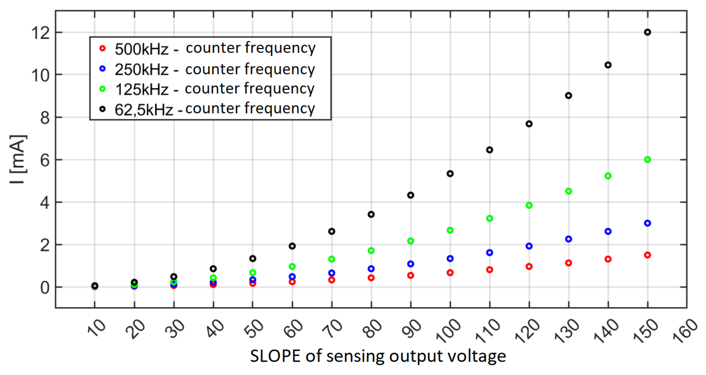
is the counter switching frequency. The calculated measurement current error
with a constant switching frequency is illustrated in
Figure 11. The lowest measurement current error was achieved with the maximum switching frequency of 500 kHz, which corresponds to 1 MHz input frequency of the measurement system.
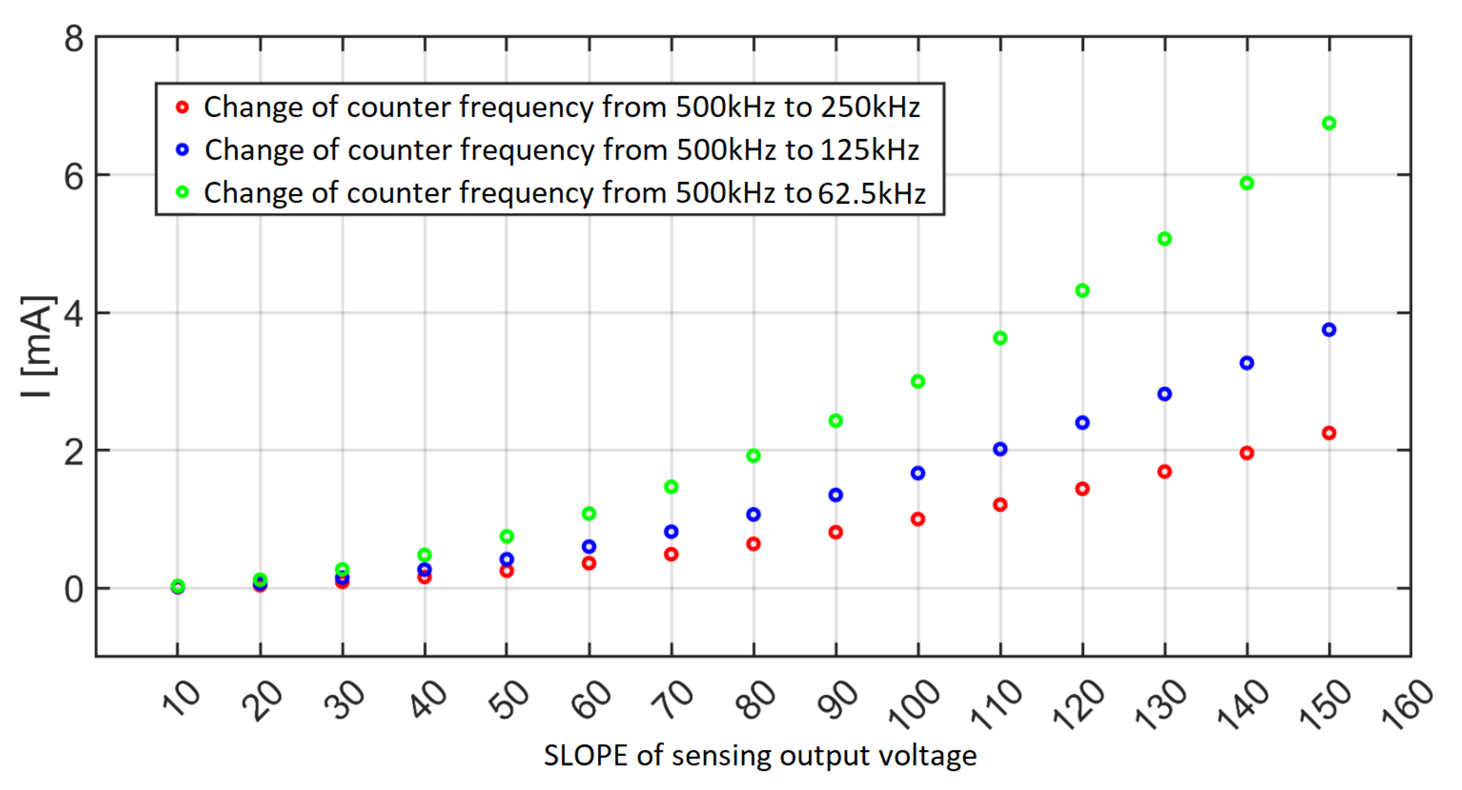
The measurement current error when the counter switching frequency is changed is calculated using Equation (
8), where
represents the initial switching frequency of
, and
is the changed switching frequency that depends on the SLOPE of sensed output voltage and it is set to determine the range corresponding to the switching frequency. The most favorable results were obtained with the switching frequency changed from 500 kHz to 250 kHz, as shown in
Figure 12.
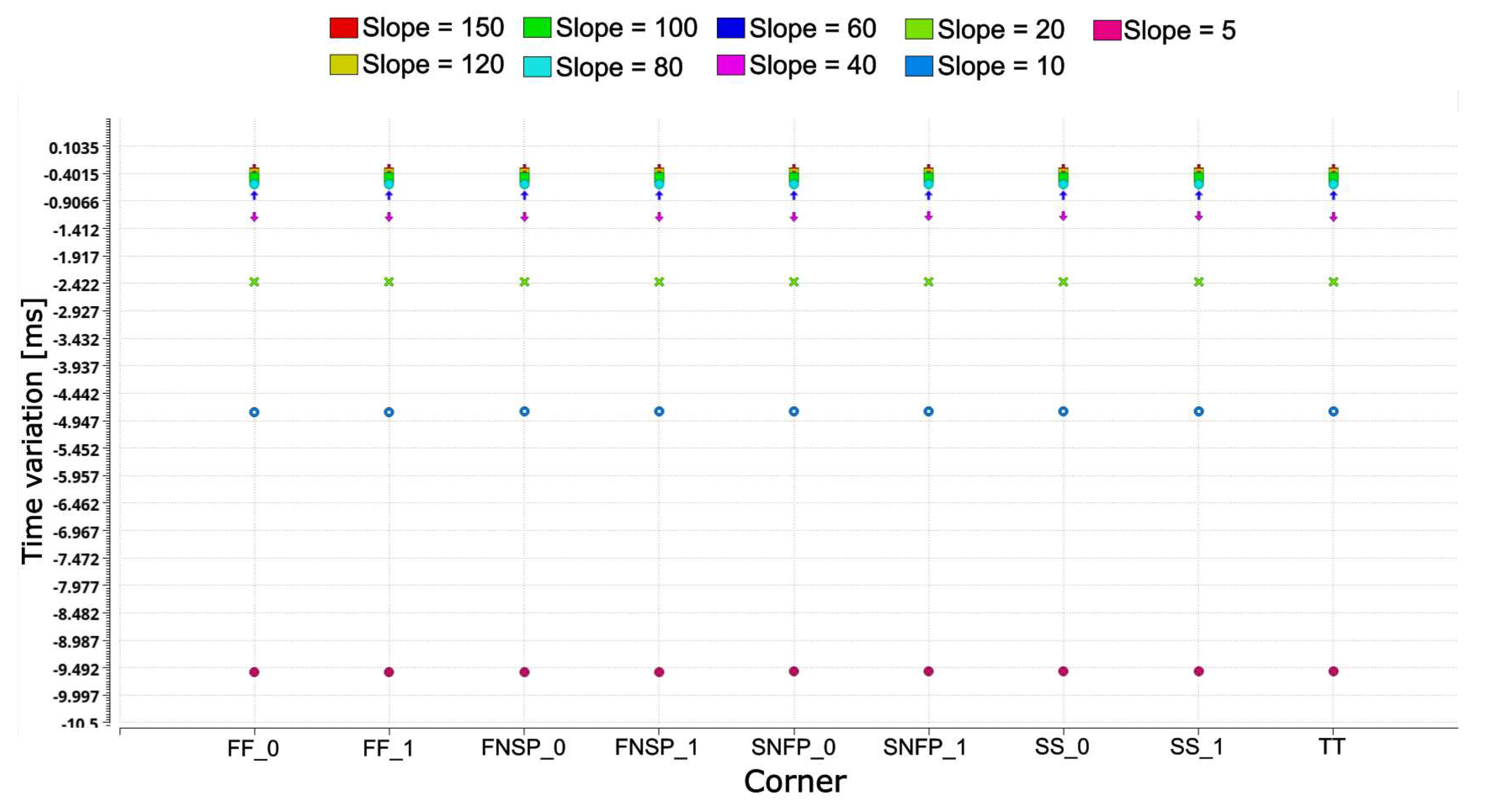
To further examine robustness of the proposed slope detector, variations of the time window were analyzed across all process corners and the entire temperature range.
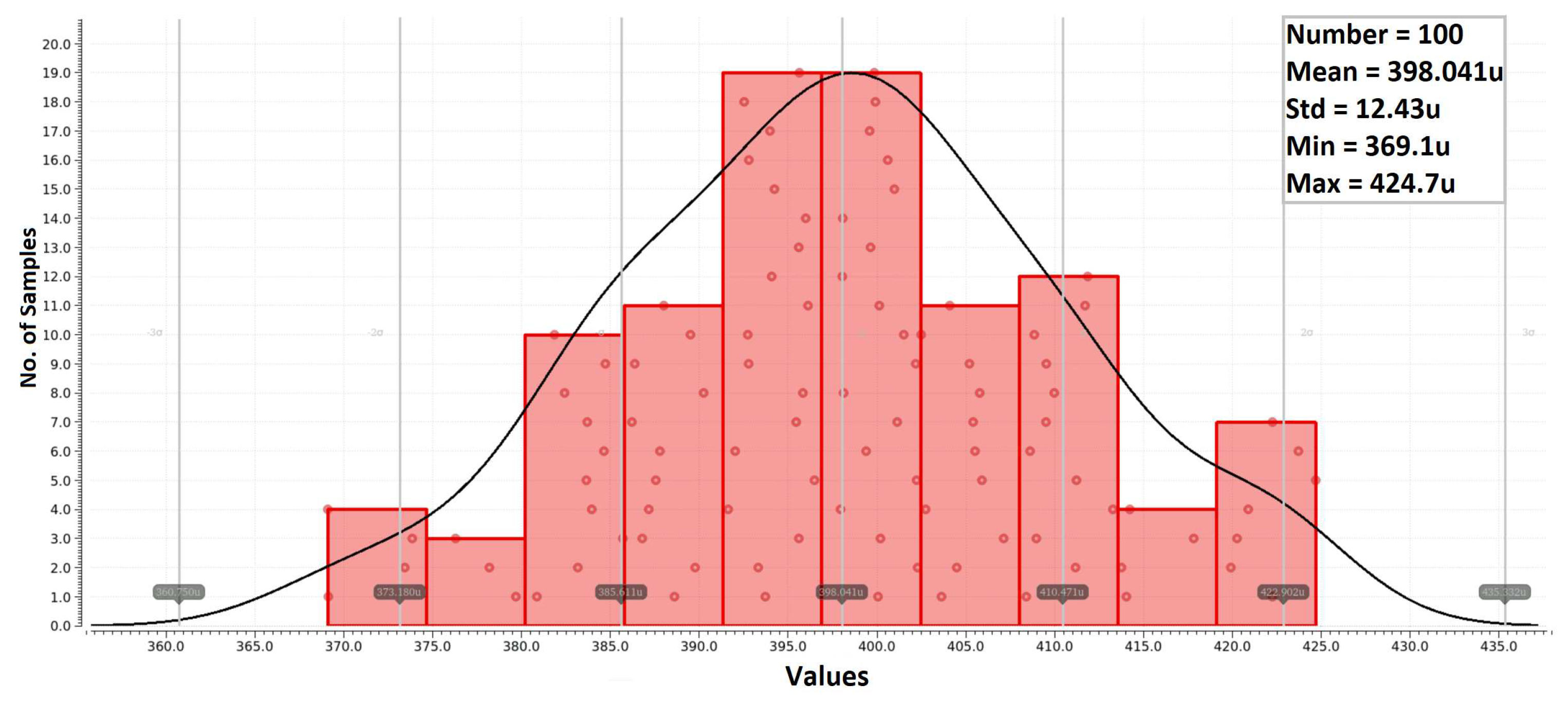
Figure 13 shows the time window variation for different slope values. As one can observe, the absolute value of the time window differs for various slope values, but it remains consistent across different process corners. However, device mismatch within K1 and K2 can introduce additional measurement errors, necessitating the use of sophisticated layout techniques. Monte Carlo analysis of the time window variation for a slope of 150V/s is depicted in
Figure 14. The time window value can fluctuate within the range from 369.1
to 424.7
, with a mean value of 398.041
. For this analysis, variations of
was considered.
Figure 15 presents physical layout of the developed slope detector circuit. The implemented layout has dimensions of 62
m x 265
m, resulting in an occupied chip area of 0.016 mm
. Both comparators essentially contribute to the total area. On the other hand, they also incorporate additional functionalities, such as hysteresis tuning and calibration features, necessary for testing the fabricated chip samples.
5. ASIC Evaluation and Measurement Results
The slope detector circuit was designed using the hardware description language (HDL) Verilog. An experimental ASIC was fabricated using a general-purpose 65 nm CMOS process. The required measurement circuits were integrated onto the same chip alongside the ASIC system. Vital and significant points of the ASIC were linked to external measurement circuits that were implemented on the test board. A developed digital logic unit controls the entire system on the chip and the measurement process. The presence of this control logic facilitates the experimental verification process and also reduces the number of required package pins, resulting in greater efficiency. Additionally, the control logic has the capability to adjust specific parameters of the circuit, such as hysteresis in comparators K1 and K2.
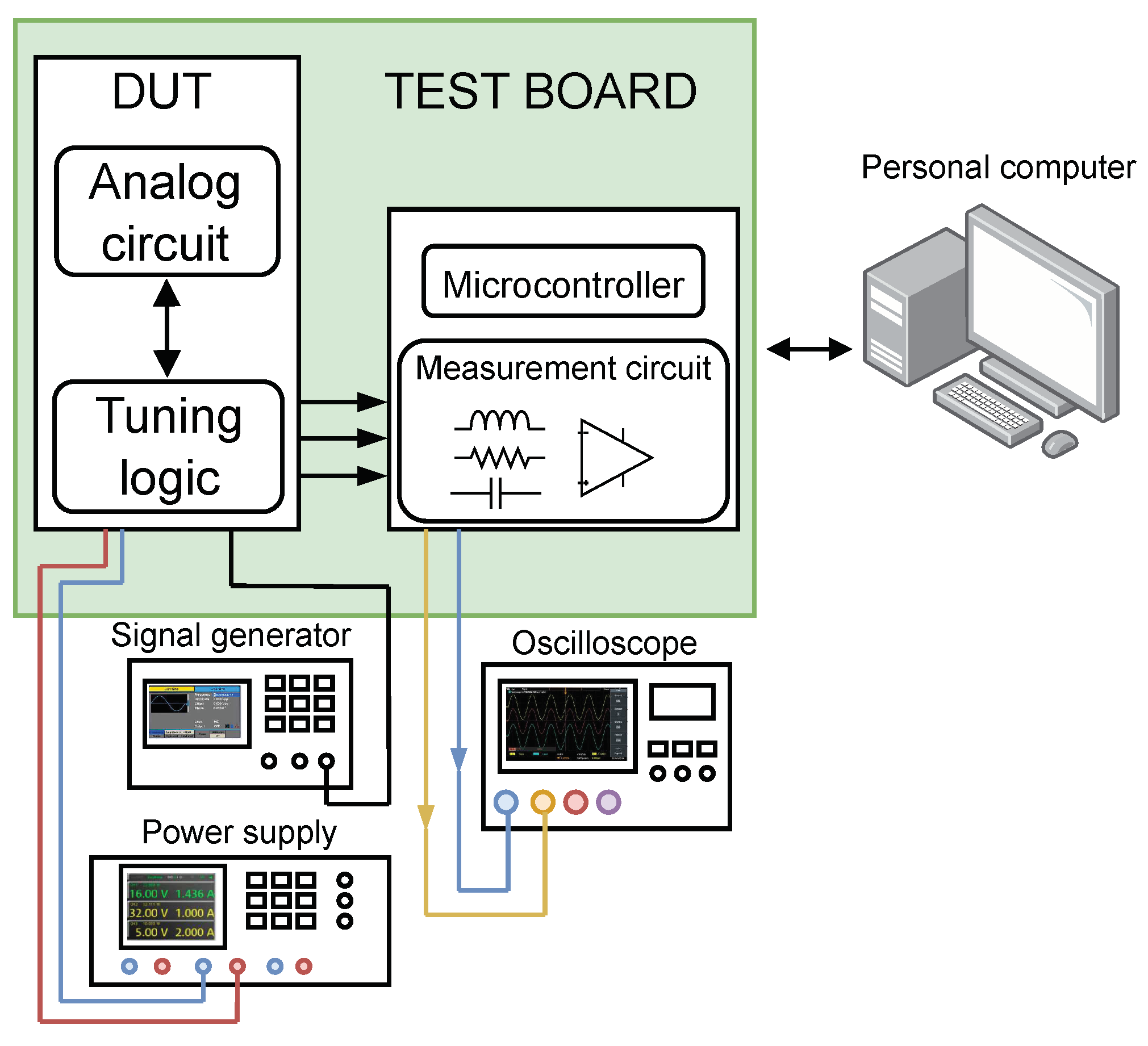
The block diagram of the entire measurement setup is depicted in
Figure 16. For this setup, the following equipment was used: Keysight InfiniVision DSOX2054 4-channel digital storage oscilloscope with 5 GSPS and 500 MHz of bandwidth, Keysight 33600A Series Waveform Generator, and Rohde & Schwarz HMC 8043 3-channel power supply.
Table 2 displays the measured conversion table, which shows the relationship between slope of the output sensed voltage, the input switching frequency of the counter, and the corresponding finite counter value. The input conditions used for measurements were identical to those used in simulations. The slope was varied from 10 to 150, and the switching frequency was set to 500 kHz, 250 kHz, and 125 kHz. Additionally, an adaptive frequency was used, depending on the set range corresponding to the specific slope value. When comparing the results obtained from simulation to the measured results, some differences can be observed in the counter values. These differences may caused by various factors, such as process tolerances, noise, and other influences. The main source of error within the measurement is likely to be the mismatch between comparators K1 and K2, as this can affect the accuracy of SD circuit.
To identify the underlying reasons for the error, conducting a comprehensive investigation of the implemented comparators in the SD circuit through precise measurements of delay and hysteresis characteristics is of utmost importance. To verify the results, we performed the measurement for five different chip samples.
The measured time delays of comparators K1 and K2 are depicted in
Table 3. The error of time window, caused by the time delay of comparators, was calculated by determining the time difference between the rising edge of comparator K1 and the falling edge of comparator K2. This time difference represents the delay of time window, and can impact the overall accuracy of measurement. The worst case is observed in chip 3, where the time difference between the rising edge of comparator K1 and the falling edge of comparator K2 results in the largest error in the time window of 994 ns. Such a value of delay have only a negligible impact on measurement results, especially when the input frequency of 500 kHz is used. In such cases, the delay is relatively small compared to the period of input signal, and its influence on the measurement accuracy can be neglected.
In
Table 4 and
Table 5, one can find the measurement results of hysteresis for comparators COM_L (K1) and COMP_H (K2), respectively. Hysteresis was measured for the slope values of 10 and 150, encompassing both the rising and falling edges of the comparators. The total error in the finite counter value, taking into account the switching frequency and the slope, is presented in
Table 6. These errors represent variations in the width of time window due to the differences in hysteresis between rising edge COM_L and falling edge of COMP_H. The best outcomes were attained in the case of SLOPE 10 for Chip1 and Chip5, and SLOPE 150 for Chip4 and Chip5. As can be observed, reducing the switching frequency leads to a decrease in the total measurement error. However, it is important to note that this reduction in error comes at the cost of diminished measurement accuracy.
6. Conclusions
A novel indirect strategy for on-chip current sensing, utilizing measurement of the output voltage slope, is introduced. However, it is essential to guarantee a high degree of device matching to minimize discrepancies leading to the measurement error and enhance the overall precision of current measurement. Thus, further improvement can be reached by employing calibration/trimming of the input voltage offset of the comparator circuits used in SD. The time delay of comparator suggests that this delay has no significant influence on the measurement accuracy and can be considered negligible. Nevertheless, the varying hysteresis values of comparators may lead to differences in the width of time window, which becomes the cause of notable measurement inaccuracies. The dissimilarities in comparator hysteresis could be caused by inadequate device matching or result from variations in the manufacturing process. The proposed measurement method and the designed SD circuit have the potential to find utility within a DC-DC converter system, providing the measurement of load current or helping approximate the output current. This application can significantly enhance control of the entire converter and improve its conversion efficiency. As for the future, our primary goal will include enhancing the design of K1 and K2 comparators, aiming to the improvement of durability and precision of the applied indirect technique for electric current measurement.
Acknowledgments
This work was supported in part by grants VEGA 1/0731/20 and VEGA 1/0760/21, and the Slovak Research and Development Agency under grant APVV-19-0392. This work has also received funding from the Electronic Components and Systems for European Leadership Joint Undertaking under grant agreement No 876868. This Joint Undertaking receives support from the European Union’s Horizon 2020 research and innovation programme and Germany, Slovakia, Netherlands, Spain, Italy.
References
- Coruh, N.; Urgun, S.; Erfidan, T. Design and implementation of flyback converters. In Proceedings of the 2010 5th IEEE conference on industrial electronics and applications. IEEE, 2010, pp. 1189–1193.
- Forghani-Zadeh, H.P.; Rincon-Mora, G.A. Current-sensing techniques for DC-DC converters. In Proceedings of the The 2002 45th Midwest Symposium on Circuits and Systems, 2002. MWSCAS-2002. IEEE, 2002, Volume 2, pp. II–II.
- Arar, S. Using Single-Ended Amplifiers in Low-Side Current Sensing: Error Sources and Layout Tips - Technical Articles, 2021.
- Lee, C.F.; Mok, P.K. A monolithic current-mode CMOS DC-DC converter with on-chip current-sensing technique. IEEE J. -Solid-State Circuits 2004, 39, 3–14. [Google Scholar] [CrossRef]
- Kim, Y.S.; No, B.M.; Min, J.S.; Al-Sarawi, S.; Abbott, D. On-chip current sensing circuit for current-limited minimum off-time PFM boost converter. In Proceedings of the 2009 International SoC Design Conference (ISOCC). IEEE, 2009, pp. 544–547.
- Xiao, Y.; Cao, J.; Chen, J.; Spring, K. Current sensing trench power MOSFET for automotive applications. In Proceedings of the Twentieth Annual IEEE Applied Power Electronics Conference and Exposition, 2005. APEC 2005. IEEE, 2005, Volume 2, pp. 766–770.
- Takaya, H.; Miyagi, K.; Hamada, K. Current-sensing power MOSFETs with excellent temperature characteristics. In Proceedings of the 2009 21st International Symposium on Power Semiconductor Devices & IC’s. IEEE, 2009, pp. 73–76.
- Huang, C.Y.; Liang, T.J.; Chen, K.H.; Li, C.Y. Primary-side feedback control IC design for flyback converter with energy saving burst mode. In Proceedings of the 2018 IEEE Applied Power Electronics Conference and Exposition (APEC), 2018, pp. 2054–2061. [CrossRef]
- Wu, K.C. Switch-Mode Power Converters: Design and Analysis; Elsevier, 2005.
- Maniktala, S. Switching Power Supplies A-Z; Elsevier, 2012.
- Billings, K.; Morey, T. Switchmode Power Supply Handbook; McGraw-Hill Education, 2011.
- Taneri, M.C.; Genc, N.; Mamizadeh, A. Analyzing and comparing of variable and constant switching frequency flyback DC-DC converter. In Proceedings of the 2019 4th International Conference on Power Electronics and their Applications (ICPEA). IEEE, 2019, pp. 1–5.
- Mohammed, A.A.; Nafie, S.M. Flyback converter design for low power application. In Proceedings of the 2015 International conference on computing, control, networking, electronics and embedded systems engineering (ICCNEEE). IEEE, 2015, pp. 447–450.
Figure 1.
Typical topology of Flyback converter
Figure 1.
Typical topology of Flyback converter
Figure 2.
Principle of the proposed approach to converter load current sensing
Figure 2.
Principle of the proposed approach to converter load current sensing
Figure 3.
Block diagram of the controller in Flyback converter
Figure 3.
Block diagram of the controller in Flyback converter
Figure 4.
Output voltage slope detection principle
Figure 4.
Output voltage slope detection principle
Figure 5.
Block diagram of the slope detector circuit
Figure 5.
Block diagram of the slope detector circuit
Figure 6.
Operation of the SD circuit
Figure 6.
Operation of the SD circuit
Figure 7.
Dependence of the counter finite value on the sensed voltage slope
Figure 7.
Dependence of the counter finite value on the sensed voltage slope
Figure 8.
Monte Carlo analysis: for slope=150 V/s
Figure 8.
Monte Carlo analysis: for slope=150 V/s
Figure 9.
error for slope=150 V/s
Figure 9.
error for slope=150 V/s
Figure 10.
Monte Carlo analysis: error for slope=150 V/s
Figure 10.
Monte Carlo analysis: error for slope=150 V/s
Figure 11.
Calculated current measurement error I[mA] for different values of counter frequency kept constant during measurement
Figure 11.
Calculated current measurement error I[mA] for different values of counter frequency kept constant during measurement
Figure 12.
Calculated current measurement error for counter frequency change within a certain range during measurement
Figure 12.
Calculated current measurement error for counter frequency change within a certain range during measurement
Figure 13.
Variations of time window over process corners
Figure 13.
Variations of time window over process corners
Figure 14.
Monte Carlo analysis: Variations of time window
Figure 14.
Monte Carlo analysis: Variations of time window
Figure 15.
Layout of the developed slope detector
Figure 15.
Layout of the developed slope detector
Figure 16.
Block diagram of measurement setup
Figure 16.
Block diagram of measurement setup
Table 1.
Calculated conversion table between the switching frequency, the slope of sensed output voltage and the finite value of counter.
Table 1.
Calculated conversion table between the switching frequency, the slope of sensed output voltage and the finite value of counter.
| |
Counter Frequency [kHz] |
| SLOPE |
500 |
250 |
125 |
62,5 |
| 10 |
3000 |
1500 |
750 |
375 |
| 20 |
1500 |
750 |
375 |
187.5 |
| 30 |
1000 |
500 |
250 |
125 |
| 40 |
750 |
375 |
187.5 |
93.8 |
| 50 |
600 |
300 |
150 |
75 |
| 60 |
500 |
250 |
125 |
62.5 |
| 70 |
428.6 |
214.3 |
107.1 |
53.6 |
| 80 |
375 |
187.5 |
93.8 |
46.9 |
| 90 |
333.3 |
166.7 |
83.3 |
41.7 |
| 100 |
300 |
150 |
75 |
37.5 |
| 110 |
272.7 |
136.4 |
68.2 |
34.1 |
| 120 |
250 |
125 |
62.5 |
31.3 |
| 130 |
230.8 |
115.4 |
57.7 |
28.8 |
| 140 |
214.3 |
107.1 |
53.6 |
26.8 |
| 150 |
200 |
100 |
50 |
25 |
Table 2.
Measured relation between counter frequency, SLOPE of sensed output voltage, and finite value of counter.
Table 2.
Measured relation between counter frequency, SLOPE of sensed output voltage, and finite value of counter.
| SLOPE |
500 |
250 |
125 |
Adaptive Frequency |
| 10 |
3122 |
1338 |
826 |
808 |
| 20 |
1456 |
949 |
476 |
627 |
| 30 |
1169 |
645 |
333 |
555 |
| 40 |
911 |
438 |
241 |
510 |
| 50 |
774 |
389 |
194 |
470 |
| 60 |
623 |
332 |
164 |
438 |
| 70 |
534 |
256 |
133 |
407 |
| 80 |
481 |
241 |
122 |
395 |
| 90 |
443 |
210 |
111 |
379 |
| 100 |
389 |
193 |
98 |
350 |
| 110 |
348 |
175 |
88 |
332 |
| 120 |
322 |
134 |
82 |
318 |
| 130 |
298 |
149 |
76 |
302 |
| 140 |
272 |
136 |
69 |
277 |
| 150 |
246 |
124 |
64 |
249 |
Table 3.
Time delay of comparators K1 and K2
Table 3.
Time delay of comparators K1 and K2
| |
COMP_L
Delay [us]
|
COMP_H
Delay [us]
|
Delay Error [ns] |
| |
Rising edge |
Falling edge |
Rising edge |
Falling edge |
COMP_L(Rising egde) - COMP_H(Falling edge) |
| Chip1 |
1.613 |
1.165 |
2.822 |
1.089 |
524 |
| Chip2 |
2.054 |
1.1 |
1.89 |
1.170 |
884 |
| Chip3 |
2 |
1.028 |
1.765 |
1.006 |
994 |
| Chip4 |
1.9 |
1.034 |
1.983 |
1.056 |
846 |
| Chip5 |
1.388 |
1.208 |
3.282 |
0.750 |
638 |
Table 4.
Measurement results: hysteresis of comparator across chip samples
Table 4.
Measurement results: hysteresis of comparator across chip samples
| COMP_L |
|---|
| |
HYS - SLOPE 10 |
HYS - SLOPE 150 |
| |
Rising edge |
Falling edge |
Rising edge |
Falling edge |
| |
HYS [mV] |
Time [us] |
HYS [mV] |
Time [us] |
HYS [mV] |
Time [us] |
HYS [mV] |
Time [us] |
| Chip1 |
15.2 |
1320 |
19.2 |
1680 |
7 |
36 |
14 |
87 |
| Chip1 |
10.4 |
944 |
14.8 |
1340 |
9.6 |
64 |
17.2 |
110 |
| Chip3 |
10 |
840 |
16.4 |
1370 |
3.2 |
256 |
9.6 |
780 |
| Chip4 |
10 |
836 |
15.6 |
1270 |
8.8 |
49 |
17.2 |
106 |
| Chip5 |
6.4 |
560 |
9.6 |
860 |
5.5 |
27 |
12.8 |
84 |
Table 5.
Measurement results: hysteresis of comparator across evaluated chip samples
Table 5.
Measurement results: hysteresis of comparator across evaluated chip samples
| COMP_H |
|---|
| |
HYS - SLOPE 10 |
HYS - SLOPE 150 |
| |
Rising edge |
Falling edge |
Rising edge |
Falling edge |
| |
HYS [mV] |
Time [us] |
HYS [mV] |
Time [us] |
HYS [mV] |
Time [us] |
HYS [mV] |
Time [us] |
| Chip1 |
20 |
1620 |
13.6 |
1250 |
20.8 |
140 |
11.6 |
74 |
| Chip1 |
11.2 |
880 |
5.6 |
520 |
12.4 |
84 |
3.6 |
24 |
| Chip3 |
7.6 |
700 |
2.4 |
160 |
10 |
62 |
1.6 |
8 |
| Chip4 |
14 |
1200 |
10 |
920 |
16 |
101 |
7.6 |
50 |
| Chip5 |
8 |
680 |
6 |
490 |
11.2 |
70 |
4 |
20 |
Table 6.
Error in the finite counter value for the different switching frequency and slope values.
Table 6.
Error in the finite counter value for the different switching frequency and slope values.
| |
SLOPE 10 |
SLOPE 150 |
| |
500kHz |
250kHz |
125kHz |
500kHz |
250kHz |
125kHz |
| Chip1 |
35 |
17.5 |
8.75 |
19 |
9.5 |
4.75 |
| Chip2 |
212 |
106 |
53 |
20 |
10 |
5 |
| Chip3 |
340 |
170 |
85 |
124 |
62 |
31 |
| Chip4 |
42 |
21 |
10.5 |
0.5 |
0.25 |
0.125 |
| Chip5 |
35 |
17.5 |
8.75 |
3.5 |
1.75 |
0.875 |
|
Disclaimer/Publisher’s Note: The statements, opinions and data contained in all publications are solely those of the individual author(s) and contributor(s) and not of MDPI and/or the editor(s). MDPI and/or the editor(s) disclaim responsibility for any injury to people or property resulting from any ideas, methods, instructions or products referred to in the content. |
© 2023 by the authors. Licensee MDPI, Basel, Switzerland. This article is an open access article distributed under the terms and conditions of the Creative Commons Attribution (CC BY) license (http://creativecommons.org/licenses/by/4.0/).
