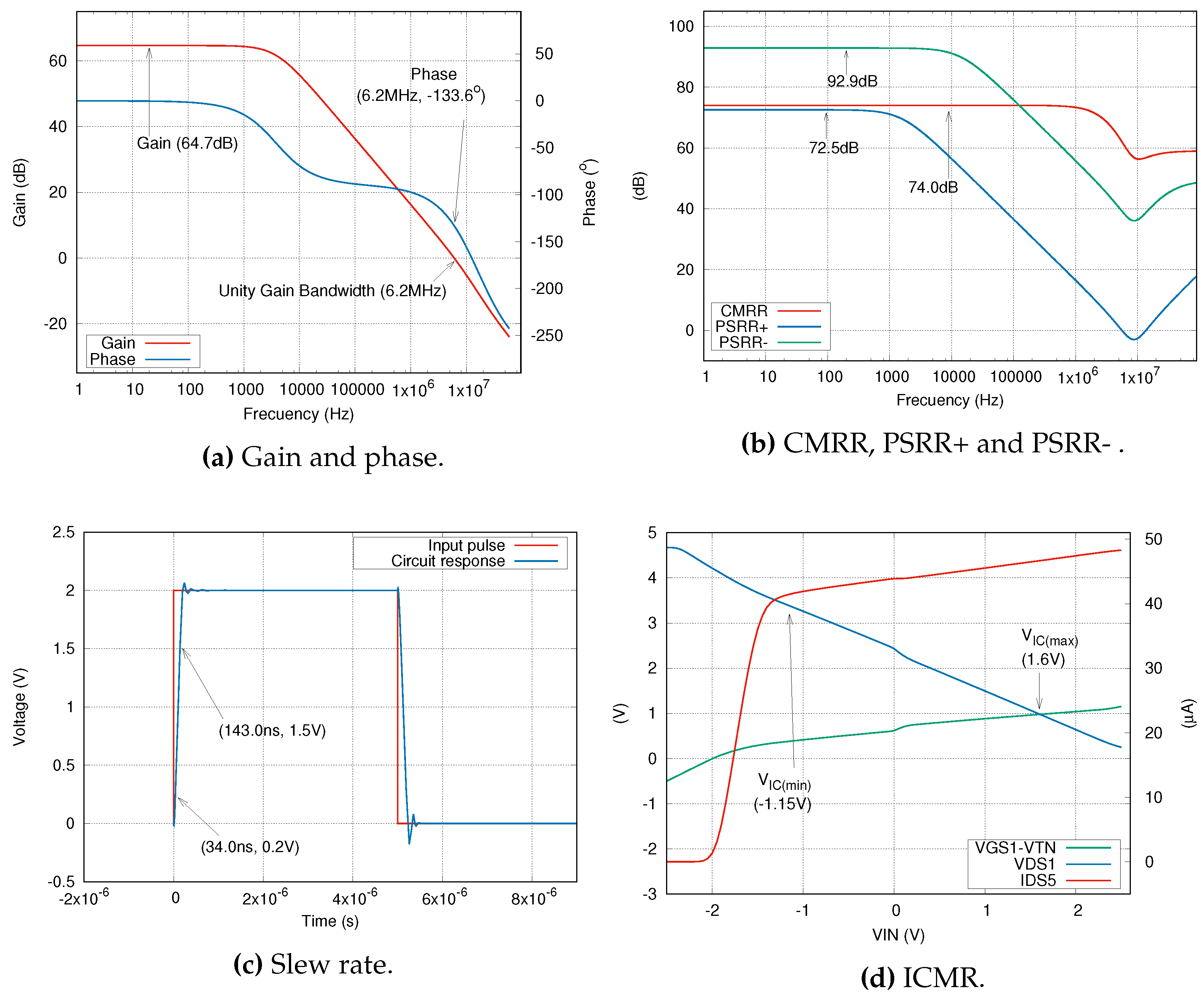
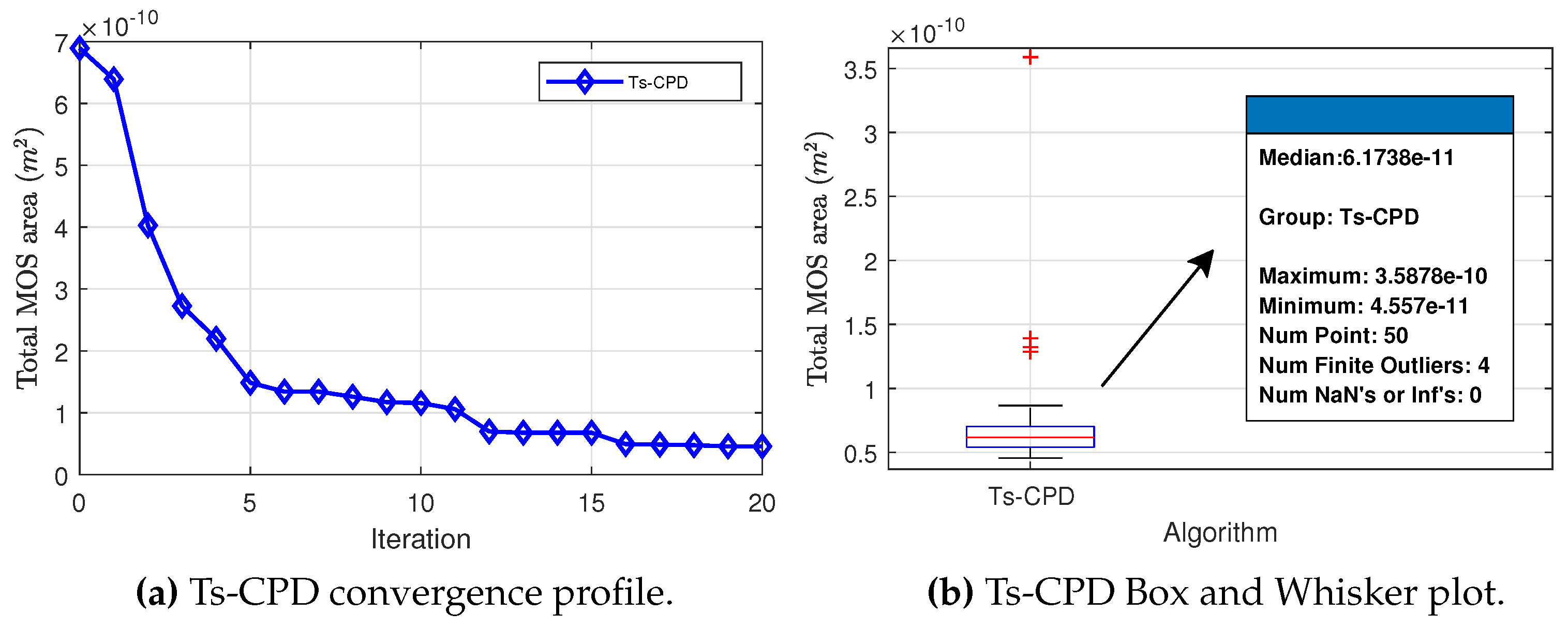
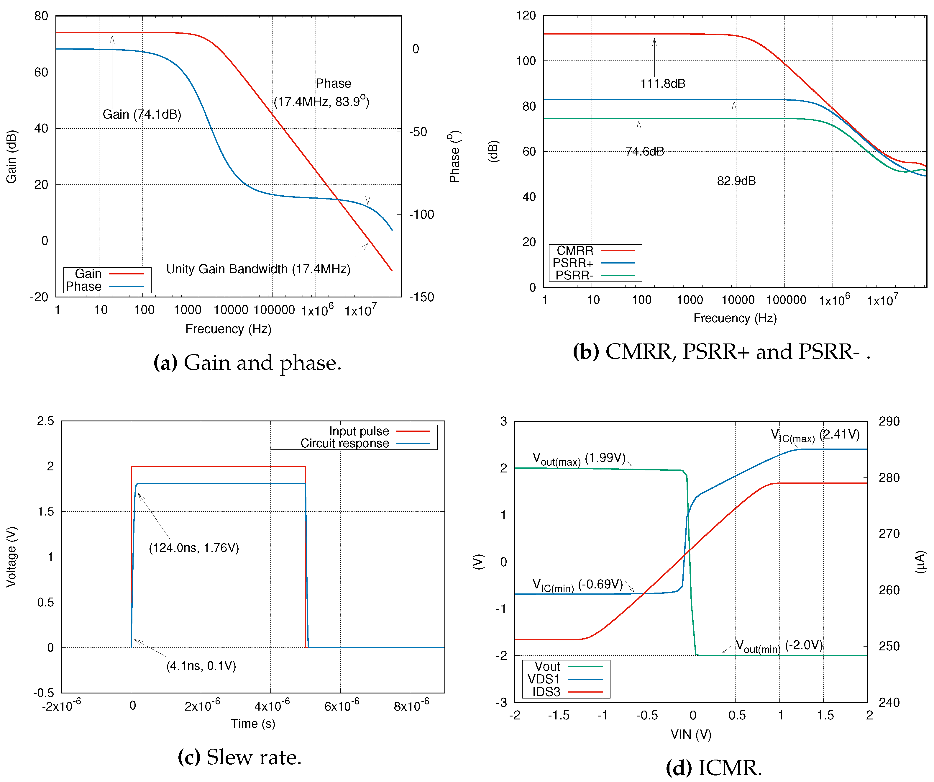
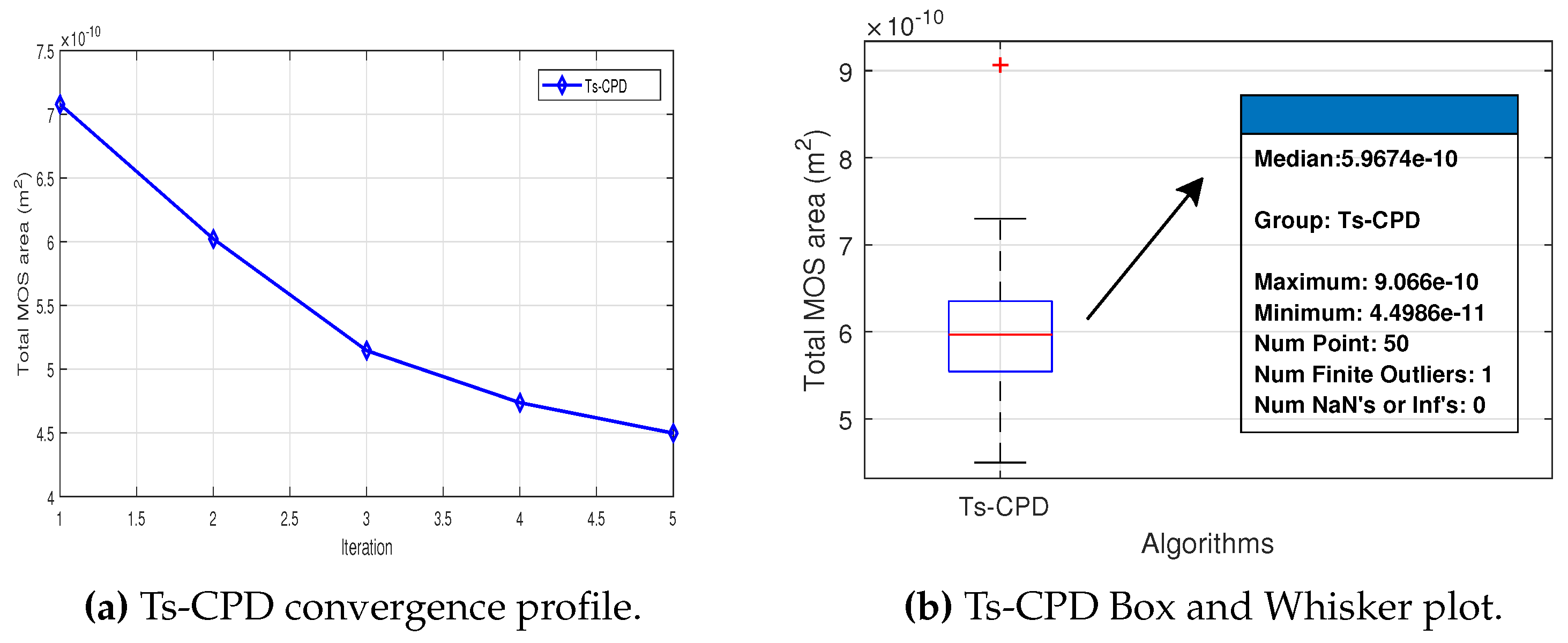
1. Introduction
In recent years, analog circuit design has received much attention, particularly those with Very Large Scale of Integration (VLSI), because optimization is a process that involves many conflicting constraints and a wide range of parameters [
1]. Therefore, it is necessary to develop more robust Computer-Aided Design (CAD) and Electronic Design Automation (EDA) tools, which increase productivity and quality and minimize design costs [
2].
The design of analog circuits comprises three major stages: selecting a topology, sizing components, and layout extraction [
3]. In the case of sizing, it is possible to use the experience when the circuits are small, but manual circuit-sizing in analog design is a time-consuming process [
4]. When the circuit grows, it is impossible to size the components solely by experience; thus, mathematical tools are necessary to optimize the circuits. Similarly, component selection is critical in achieving a targeted performance and quality level [
5].
The complexity when manually implementing an analog project is usually weeks or months. CAD and EDA tools are used to improve the design process; today’s analog design environment is made of CAD tools for editing, evaluation, and design verification of analog integrated circuits, for example, HSPICE, SMASH, and CADENCE. Automatic analog circuit sizing based on optimization tools is divided into two main subclasses: equation-based and simulation-based circuit optimization. The first uses analytical design equations, while the second takes advantage of simulator circuits, e.g., SPICE, to provide accurate performance figures.
Critical points in optimization-based approaches are the optimization techniques and methods used to evaluate circuit performance. Different optimization techniques are used to dimension and optimize analog integrated circuits, both deterministic and stochastic. In equation-based methods, it is possible to use classical optimization methods. However, when using the circuit simulator, it is necessary to use stochastic heuristic optimization techniques [
6].
Many optimization techniques and tools for automation design have been developed over time [
7,
8]. Also, Geometric Programming was used to design a CMOS op-amp in [
9]; the authors used the transistor models called GP0 and GP1, implemented in MATLAB but validated with the HSPICE level-1 models simulation. This method is robust, although it implies using equations for the circuit and each optimization parameter. This technique is updated in [
10], where the validation is made using the BSIM3v1 model.
In addition, the fuzzy logic has been used for the circuit design as in [
11,
12], or in [
13], where a multi-objective design is presented, while in [
14], a tool for analog synthesis is introduced. In [
15], a Neuro-Fuzzy method for analog circuit design is presented; it is of easy implementation, natural understanding, and better performance than static methods of fuzzy optimization; however, it still needs the human experience in the particular circuit to be designed. In [
16], the application of an innovative algorithm of the type Customized Genetic Algorithm (CAG) is reported. Its purpose is to improve the optimization process of analog CMOS ICs.
More recently, evolutionary algorithms have been successfully applied to component value selection for analog active filters [
17,
18] and to the analog integrated circuits design as in [
19], where the sizing is achieved using a Particle Swarm Optimization (PSO) algorithm implemented in MATLAB and the results verified at the end with SPICE. In [
20], a CMOS differential amplifier and a two stages CMOS op-amp are optimized to occupy the minimal possible area by the circuits and to improve their performances using the gravitational search algorithm in combination with the particle swarm optimization (GSA-PSO). The design is formulated as an optimization problem with a single objective function, although certain manual tuning is necessary to resolve conflicts with either design or performance parameters when using this method. In the work [
21], a crazy PSO (CRPSO) is applied to improve the premature convergence to a local minimum of the PSO; the application optimizes the minimization of the total MOS area of two amplifier configurations, a two-stage PMOS type operational amplifier, and an NMOS cascade code amplifier.
A good comparison of several evolutionary methods for the synthesis of analog circuits is presented in [
22]; these are Artificial Bee Colony (ABC), PSO, and Chaotic Differential Evolution (CDE). The algorithms are implemented in MATLAB and interfaced with the WINSPICE circuits simulator. In [
23], the authors present their tool for the automation design of analog circuits based on the use of a Genetic Algorithm (GA) modified; this is a multi-objective design for CMOS op-amps. Another evolutionary algorithm used for automation design is the New Hybrid Shuffled Frog Leaping Algorithm (NHSFL) implemented in MATLAB linked with the HSPICE circuits simulator [
24]. It was tested with two examples of design, but the method can be extended to the general op-amp design according to the authors.
Heuristic techniques are necessary to solve problems with many design criteria [
25]. Although they do not guarantee finding the optimal solution exactly, they provide an acceptable approximation to it in an acceptable computation time [
26]. Therefore, another challenge for sizing high-performance analog circuits with tight specifications is the need for a powerful enough optimization kernel for EDA tools to handle tighter specifications and improve optimization capability [
27]. Different optimization kernels are currently used for EDA tools; among them, we can mention the kernels based on GA [
23], PSO [
28], ACO in [
29], SA in [
30], GSA in [
20], NSGA-II in [
31] and NSGA-II, MOPSO, and MOSA in [
32].
Most heuristic methods used in the optimization kernels of the EDA tools are based on multi-objective optimization techniques [
6,
31] or use a restriction approach with a single objective and static penalty functions. This is due to their simplicity and easy implementation, making it a relatively reliable method [
33]. Penalty functions penalize non-feasible solutions by adding a specific value to the objective function as an amount proportional to the violation of the restriction. Thus, the optimization problem is transformed into a restrictionless optimization problem. The main problem with this methodology is choosing the appropriate penalty factor for a particular problem; it is often a complicated task, but if an adequate factor is selected, a premature convergence can occur or solutions outside the feasible region can be obtained [
34]. Another approach currently used in problems with restrictions is self-adaptive penalty functions, which significantly improve the results [
35]. Unfortunately, many last-generation restricted optimization methods have yet to be introduced into EDA tools. Therefore, advanced restricted optimization methods should be applied to circuit dimensioning tools to address this challenge.
In recent years, algorithms based on cellular automata, such as CPSO [
36], CPSO-DE [
37], CCAA [
38], and MmCAA [
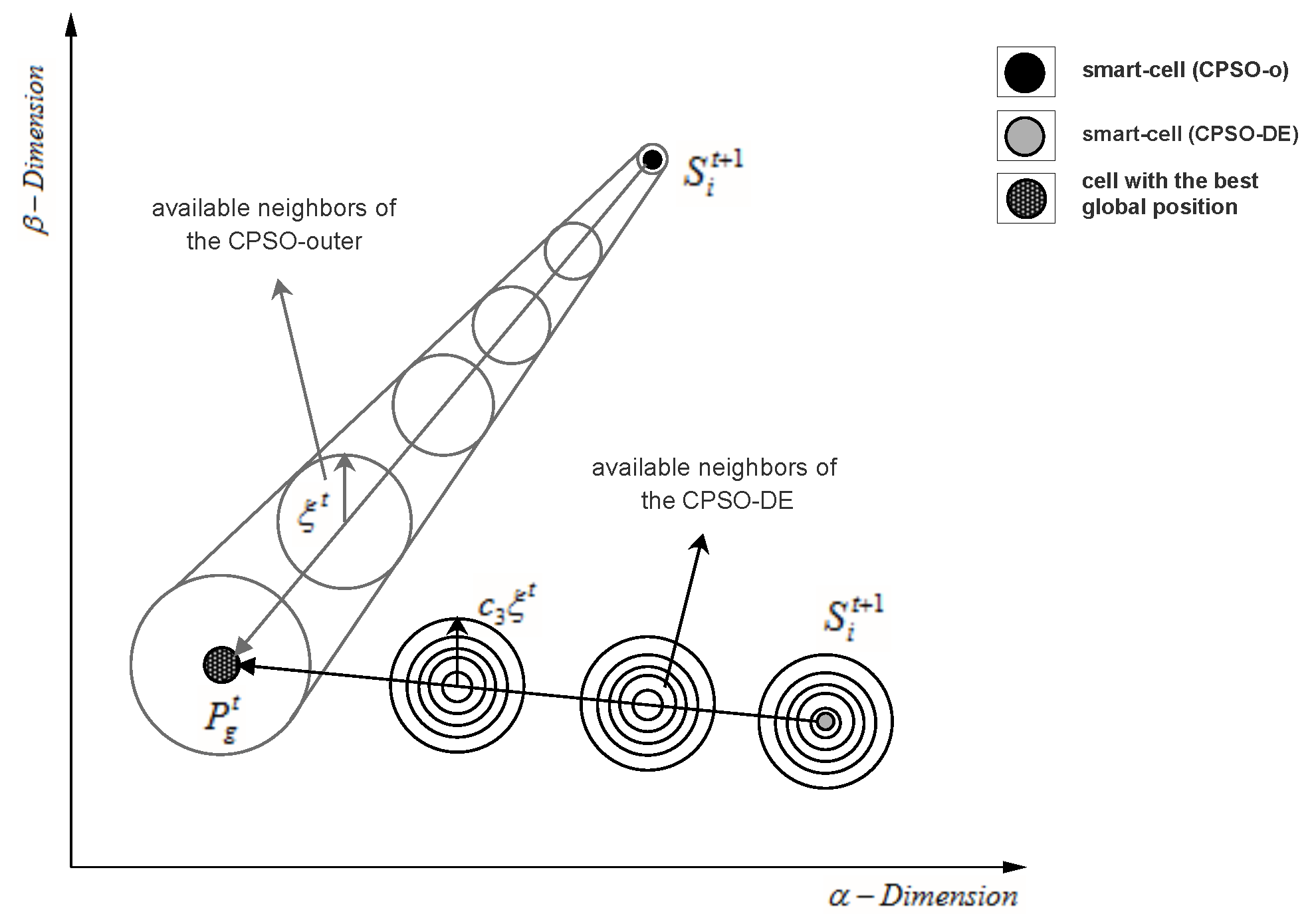
39], have shown excellent performance in solving global optimization problems, demonstrating a good balance between exploration and exploitation, as well as a good speed of convergence. Among them, the CPSO-DE has proven to be an excellent design method for identifying adaptive IIR systems due to the use of a differential evolution rule for the neighborhoods of cellular automata of the PSO that improves the balance between exploration and exploitation than the original version of the CPSO.
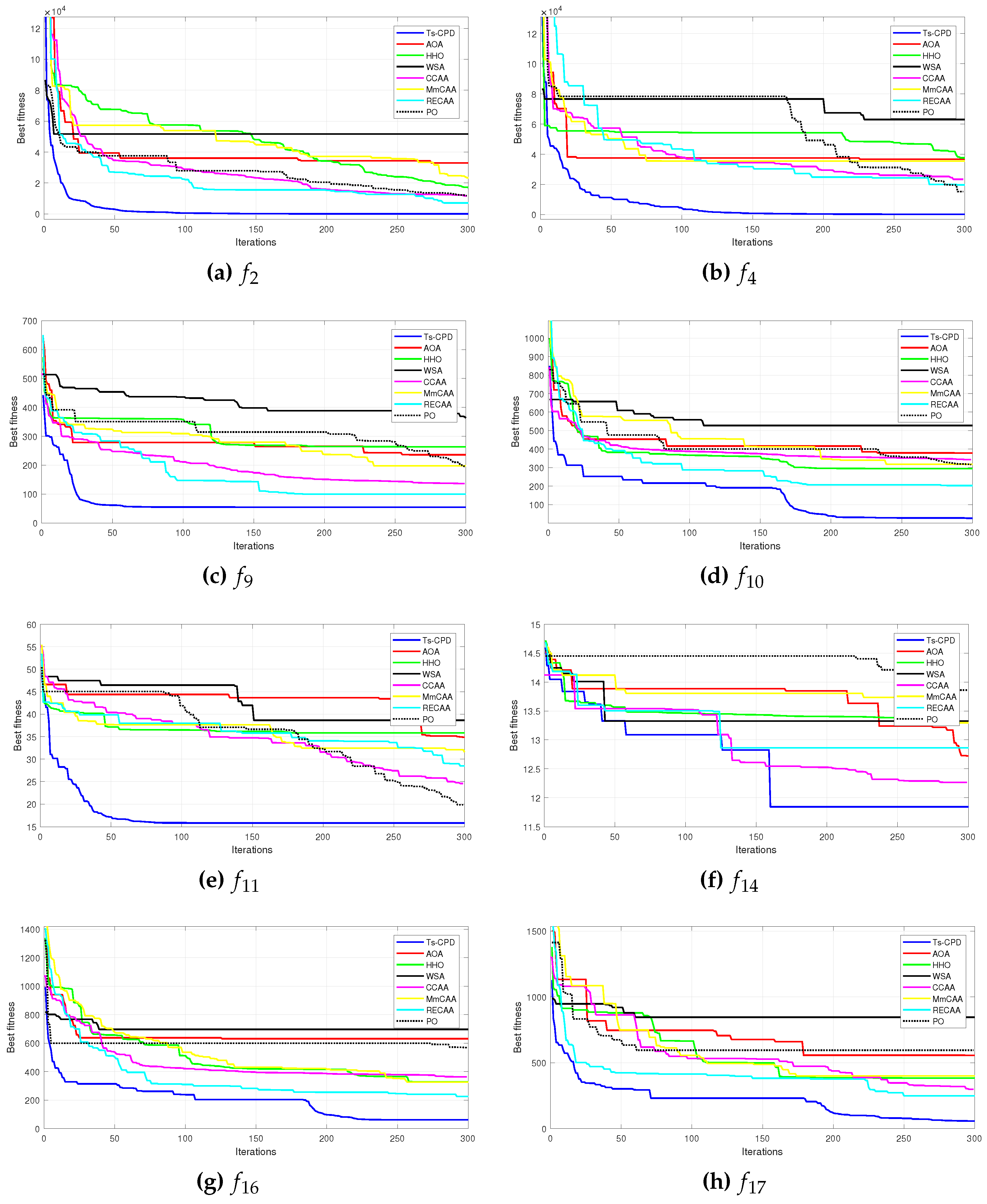
According to the previous observations, this document introduces the hybrid continuous optimization algorithm called CPSO-DE that incorporates cellular automata concepts to improve PSO exploitation capabilities with DE exploitability. The algorithm was tested on established benchmark functions (CEC 2005) [
40] against 7 recently published algorithms for global optimization, yielded satisfactory results.
Additionally, Deb’s rules were incorporated into the algorithm to address constrained optimization [
41,
42]; this algorithm is called Ts-CPD applied in a single design objective problem, for the sizing of analog circuits to improve their performance. The approach is used as the optimization core of an EDA tool to size CMOS analog circuits efficiently. In particular, we focus on diminishing the total component area as the objective. At the same time, other specifications, such as dc gain, bandwidth and power dissipation, are treated as constraints that guarantee good overall performance. The circuits chosen for testing our method are well known, which allows a comparison of results with other proposals. We implemented the optimization in Matlab while the circuit simulation was done in Ngspice. Both optimization and simulation parts are linked.
We compare our proposal with previously published works, including PSO variants such as Particle Swarm Optimization (PSO)[
19], Genetic Algorithm (GA)[
43], Harmony Search (HS)[
44], Differential Evolution (DE)[
44], Artificial Bee Colony (ABC)[
44], Gravitational Search Algorithm PSO (GSA-PSO)[
20], Geometric Programming (GP)[
9] and Aging Leader and Challenger PSO (ALC-PSO)[
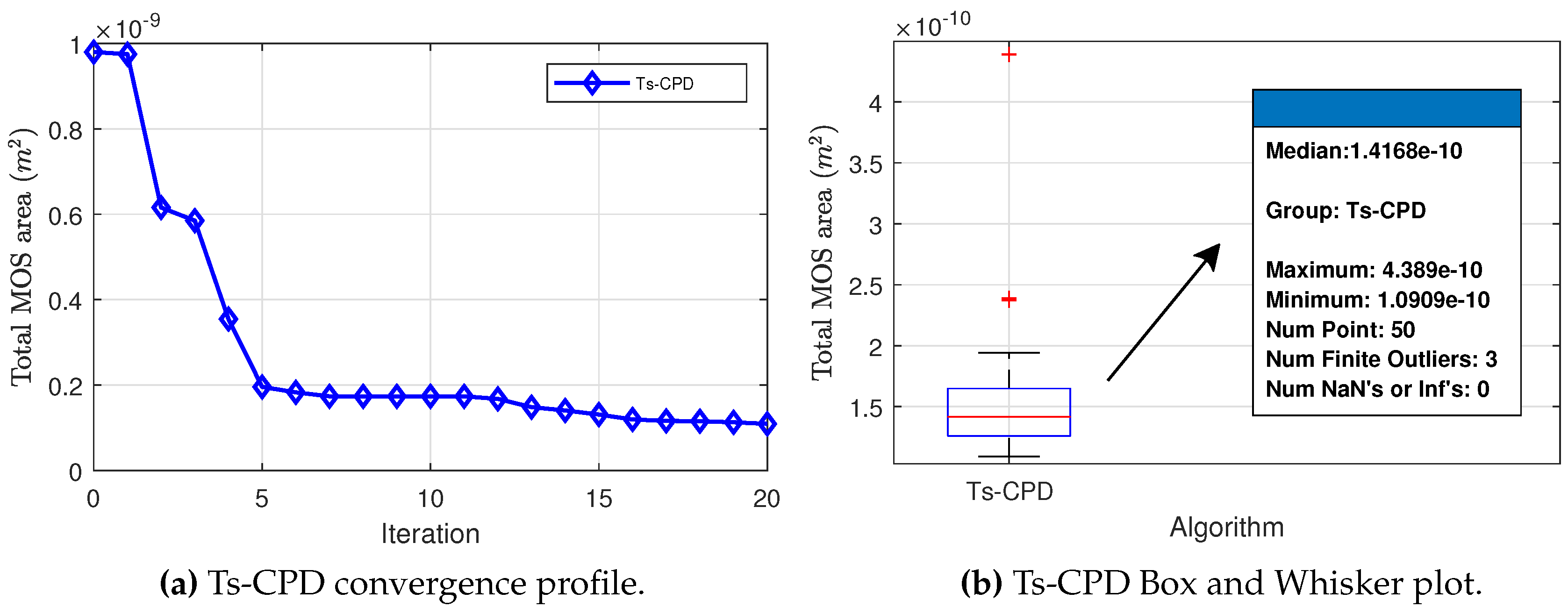
1]. The results show that Ts-CPSO can find a better circuit design solution than the above-listed approaches. In addition, it shows a rapid convergence in all the studied cases.
Overall, the proposed CPSO-DE algorithm is easy to understand, performs exceptionally well for continuous optimization, and is modified with Deb’s rules to define the Ts-CPD algorithm in order to tackle problems with multiple constraints, as demonstrated in the area optimization of CMOS analog circuits.
The rest of the paper is organized as follows:
Section 2 gives a review of CPSO-DE, while the hybridization of CPSO-DE with constrained optimization is explained in
Section 3.
Section 4 describes three circuits in terms of their design variables and constraints.
Section 5 validates the proposed Ts-CPD through three cases of study, contrasting the findings against results from previous works. Finally, this article is concluded in section 6.
4. The proposed tool for analog IC sizing
The EDA tool proposed for the designer of analog circuits through the Ts-CPD algorithm allows obtaining a minimum area of the components used while complying with the design specifications. It is handy for designing the frequency response of circuits, such as bandwidth, phase margin, CMRR, or PSRR; only the slew rate can be designed in the time domain. For this purpose, before beginning the design, the designer must introduce the specifications (restrictions) of the circuit and the acceptable ranges and values for the parameters according to the technology used. The parameters to choose are the width and length of the CMOS transistors, capacitance and resistance (if any) values, bias current, and voltage sources.
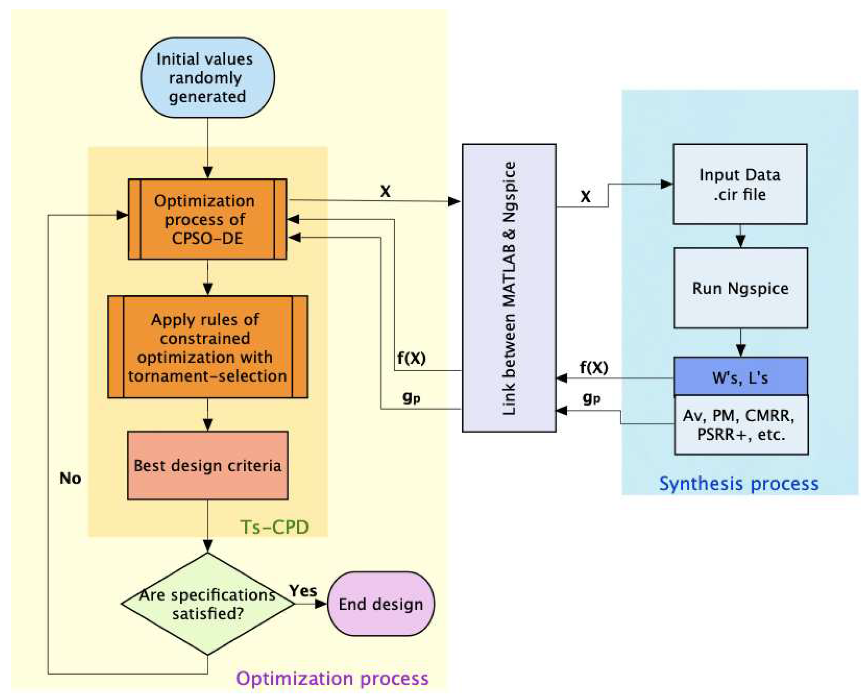
The tool consists of two main modules: the optimization and synthesis processes. The optimization process contains the Ts-CPD algorithm comprising the CPSO-DE and the Deb rule, with a new transition rule given by (
13); this module is implemented in Matlab. The synthesis process uses the specialized Ngspice software, which allows analog circuit simulations without mathematical equations. Instead, the standard configurations necessary to evaluate the performance of circuits are implemented in a netlist format. Both modules, the optimization and synthesis processes, are linked, allowing an automatic circuit design. The flow chart for our EDA tool, using Ts-CPD, is shown in
Figure 3.
The following subsection describes three case studies, in terms of their variables and constraints, that will be used to verify the efficiency of the EDA tool.
4.1. Cases of study
To test our algorithm and tool, we chose three case studies, a “CMOS Differential Amplifier" differential amplifier, a “CMOS two-stage operational amplifier," and a “CMOS folded cascode operational transconductance amplifier." These cases were chosen because they have already been studied previously, and therefore, it is possible to compare the results of our algorithm against previous results, which is very interesting. In this sense, case 1 has 5 independent variables and 11 restrictions to meet, case 2 has 5 independent variables and 11 restrictions, while case 3, the most complete, has 9 independent variables and 13 restrictions to meet at the same time.
4.1.1. Case 1: CMOS differential amplifier
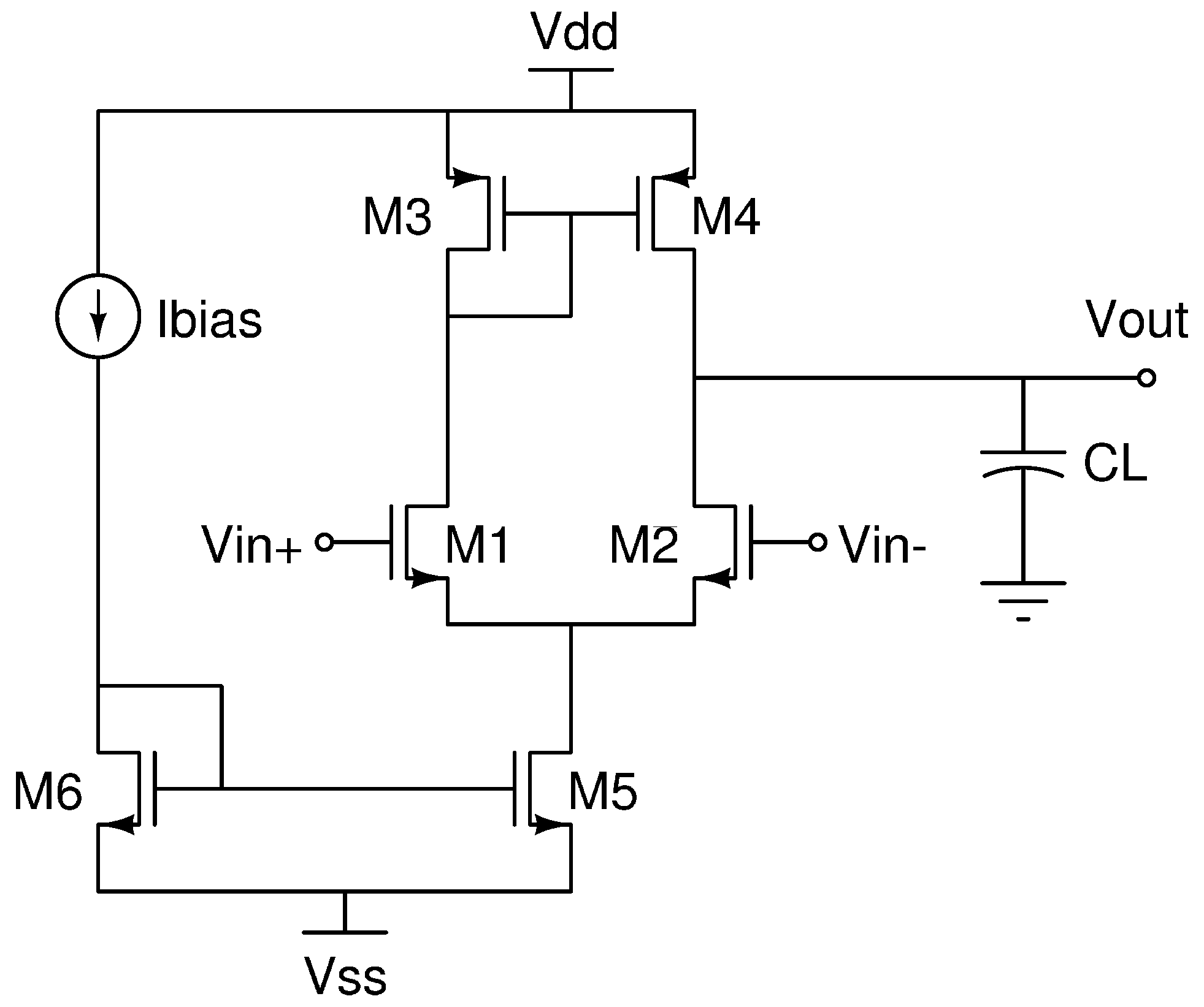
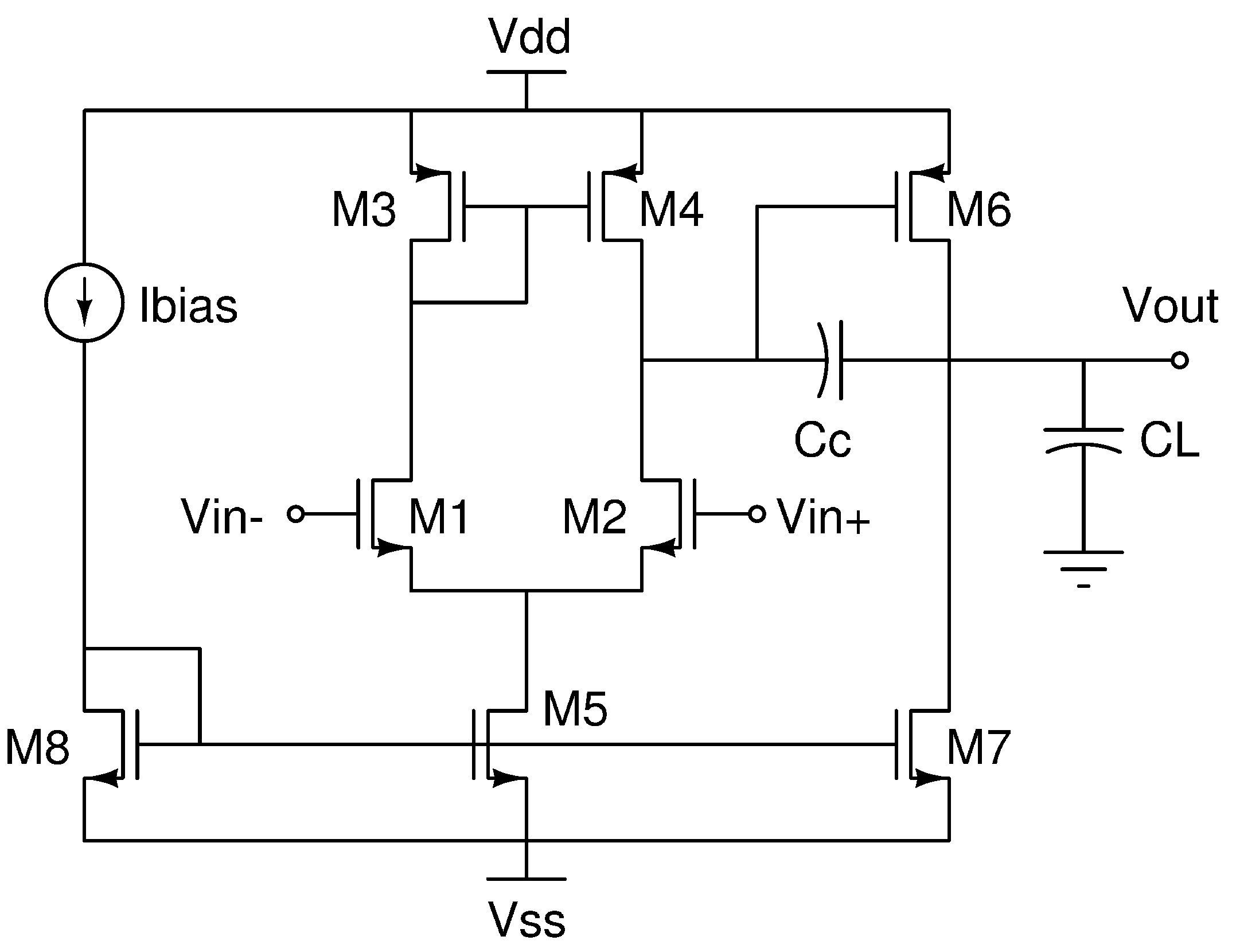
Figure 4 shows our first case of study, a CMOS differential amplifier. First,
must be equally sized than
; thus, the following equality restrictions must be satisfied:
Secondly, s of the current source,
and
, must be equally sized, too, thus
We let both
and
be independent variables, and our algorithm selects their values while
. That is because the sizes of all s are within a specific range imposed by the technology used for this design:
In our case,
was fixed to 4
m for a better comparison with other works, and
was fixed to
m to have a value large enough. For this example, there are 5 independent variables (
,
,
,
and
) and 2 dependent ones (
and
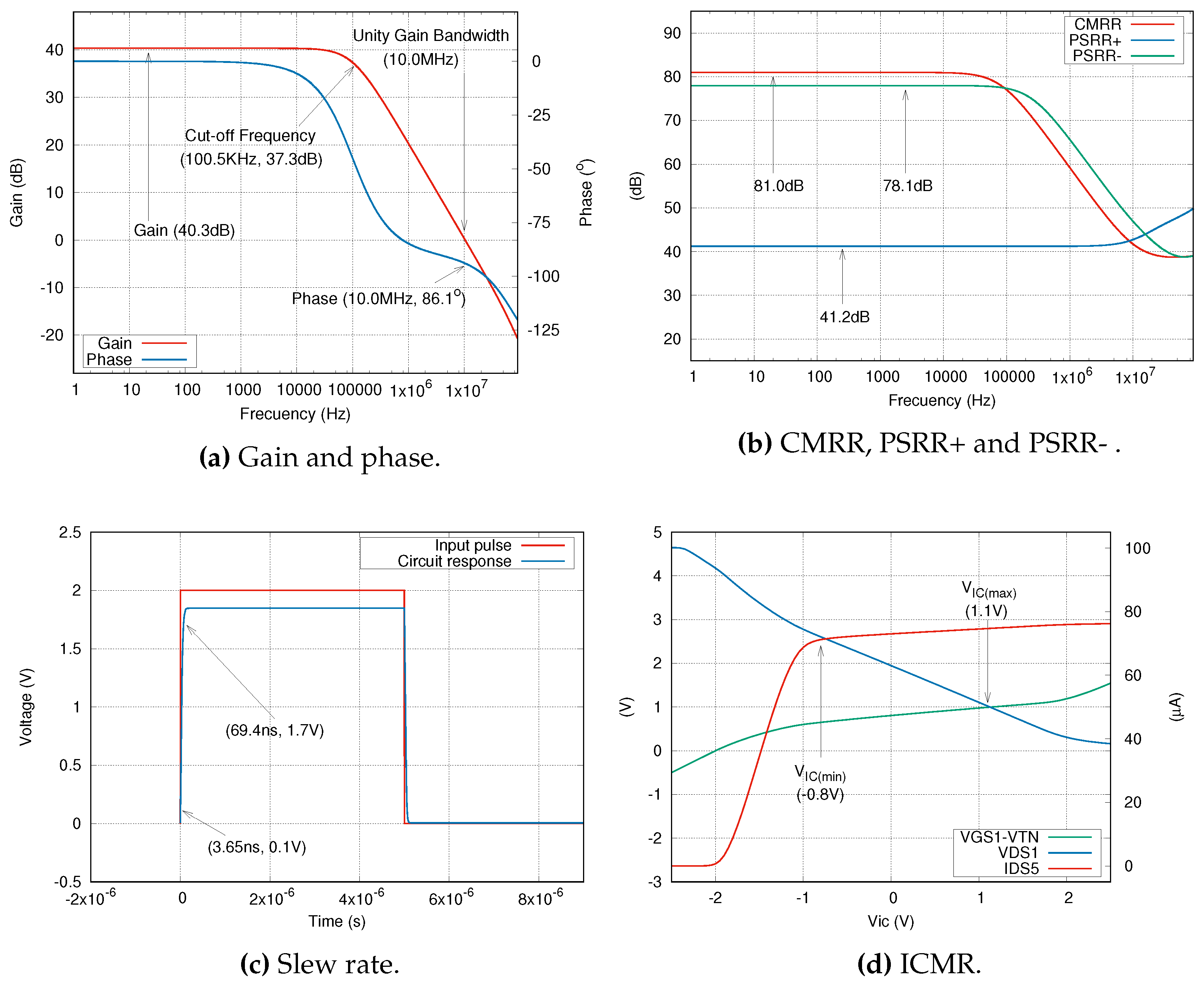
). On the other hand, the design specifications to be met will be treated as constraints. For this case, there are 11 constraints: load capacitance, slew rate, power dissipation, phase margin, cut-off frequency, DC gain,
(min),
(max), CMRR, PSRR+ and PSRR-.
4.1.2. Case 2: CMOS two-stage operational amplifier
Figure 5 shows our second case of study, a CMOS two-stage operational amplifier consisting of 8 s. The first amplification stage, differential input, has the stipulation that
must be equally sized as
, so that equations (
14), (
15) are still valid, and we add,
Also, to avoid an output offset at the second amplification stage, the following restriction is imposed:
Similarly, as in (
16), sizes of the CMOS two-stage operational amplifier are in a specific range, but now
. Also, the compensation capacitance is within a range of values, between
and
, which the designer selects:
The
and
values are fed to the Ts-CPD algorithm through a file in our EDA tool. We choose
pF, because lower values than that are challenging to achieve and
pF to avoid using significant areas, but these values are easily changed.
On the other hand, bias current
also is within a range o values:
It is clear from equations (
14), (
15) and (
17) that, for the purpose of design,
and
can be handled as independent variables, while
and
as can be handled as dependent ones.
is deduced from (
18), thus,
is also a dependent variable;
and
are considered independent variables whose values are bounded by (
20) and (
19), respectively. Therefore, this example has 5 independent variables,
and
, whose values are selected by our algorithm and 5 dependent variables
and
, whose impact over cost function and restrictions is evaluated by our algorithm to determine new values for independent variables, in an iterative process. In this paper, the length of s is considered constant. However, when lengths are considered variables, the minimum and maximum values must be established, as for widths in equation (
16). For this case, there are 11 constraints: load capacitance, slew rate, power dissipation, phase margin, unity gain bandwidth, DC gain,
(min),
(max), CMRR, PSRR+, and PSRR-.
4.1.3. Case 3: CMOS folded cascode operational transconductance amplifier
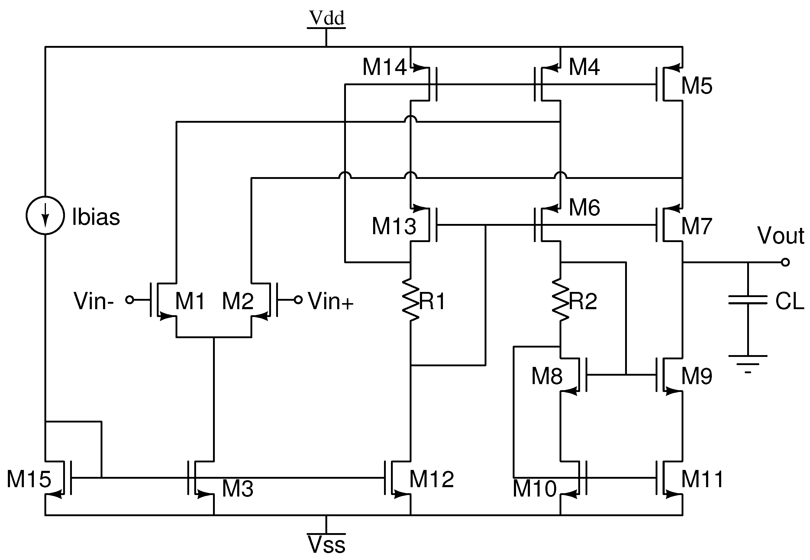
A third case of study is the folded cascode operational transconductance amplifier (FCOTA) shown in
Figure 6. The transistors
and
are equally sized; thus, equation (
14) is also valid. We considered the transistor widths
and
independent variables and
and
dependent ones, as follows:
In addition,
,
,
and
are considered independent variables while
,
,
,
, and
are considered dependent variables, as follows:
The values of the bias current
are bounded by (
20) and properly selected by our algorithm. For design, we considered
as an independent variable. Thus, our algorithm also selects its value within
, while
is considered a dependent variable, with
. This way, there are 9 independent variables (
,
,
,
,
,
,
,
and
) and 9 dependent variables (
,
,
,
,
,
,
,
and
). The constraints for this case are 13: load capacitance, slew rate, power dissipation, phase margin, unity gain bandwidth, DC gain,
(min),
(max),
(min),
(max), CMRR, PSRR+ and PSRR-.
6. Conclusions
The Ts-CPSO algorithm that was proposed and implemented improves the CPSO by incorporating a way of evaluating the performance of constraints, through the optimization-with-constraints method, with a new rule we proposed. This algorithm has the advantage of not only minimizing the objective function but also ensuring that the constraints are met and then generating the new parameter values. Then the Ts-CPSO algorithm is incorporated into our EDA tool for the optimal sizing of analog circuits, which does not require mathematical equations since the optimization is linked to a simulator that provides the circuit’s behavior.
The Ts-CPD algorithm, as part of our EDA tool, was tested with three cases of study in a 0.35um CMOS technology, a differential amplifier, a two-stage operational amplifier, and a folded cascode operational transconductance amplifier. It was proposed as a design objective to reduce the total area occupied by the transistors while complying with some established constraints. In all cases, our tool found a better solution, for the objective, than previously reported tools, while the constraints were kept within the desired limits.
In future work, we are going to implement a multi-objective algorithm, which we will add as the kernel of our EDA tool. We will also do design tests with analog circuits with more transistors and large-scale analog circuits, such as the ADC, considering the Layout design. As another potential future project, a framework incorporating multiple algorithms for optimizing various analog circuits can be developed. This framework would allow users to customize each algorithm’s parameters to enhance its performance, compare the different methods with convergence plots and identify the optimal design.
