1. Introduction
Quantum dot (QD) light-emitting diodes (QLEDs) have emerged as highly promising contenders for next-generation display and lighting applications, boasting remarkable attributes such as exceptional color purity, tunable emission wavelength, high efficiency, and solution processability [
1,
2,
3,
4,
5,
6]. Due to these outstanding optoelectronic properties and advancement in device structure, QLEDs are increasingly approaching the performance of organic light-emitting diodes (OLEDs) [
1,
2,
3,
4,
5,
6,
7,
8,
9,
10,
11].
One key factor influencing QLED performance is the selection and engineering of the various functional layers within the device structure. While the majority of QLEDs traditionally feature a bottom-emitting structure, there is a growing interest in top-emitting (TE) structures due to their versatility in various applications. One notable advantage of TE-QLEDs is their ability to minimize the influence of numerous integrated thin-film transistors on the substrate, which expands the range of compatible substrate materials, including opaque substrate. [
13]. TE structures enable the fabrication of devices on substrates such as silicon or metal foils, thus significantly widening the possibilities for display applications.
To achieve efficient light emission, optimizing charge balance is crucial, especially in QLEDs where hole injection can be relatively inefficient when compared to electron injection. This is due to the higher hole injection energy barrier and disparities in electron and hole mobility [
14,
15,
16]. An imbalance in hole and electron injection and transport can lead to QD charging and increase the likelihood of non-radiative Auger recombination [
17,
18,
19].
ZnO nanoparticles (NPs) is widely employed as the electron transport layer (ETL) in QLEDs due to their advantages, including high mobility, transparency, and suitable interface energy level [
20]. However, ZnO NPs often exhibits a significant concentration of oxygen vacancies, leading to non-radiative recombination at the QD-ZnO interface [
17,
21]. When the QD emission layer (EML) is in direct contact with ZnO NP ETL, spontaneous electron transfer occurs at the interface, resulting in exciton quenching [
22,
23]. Excitons in QD EML are susceptible to quenching through interfacial charge transfer processes and/or intragap-assisted non-radiative recombination centers [
18]. Consequently, addressing the interface between the QD EML and ZnO NP ETL is crucial to enhance device performance. One approach to alleviate exciton quenching is to insert an insulating layer between the QD EML and ZnO NP ETL. Zhang et al. reported a red QLED with a low turn-on voltage of 1.7 V, a high peak external quantum efficiency (EQE) of 20.5%, and a long lifetime of over 1,000,000 h at an initial brightness of 100 cd/m
2 [
24]. The enhanced performance is attributed to the poly(methyl methacrylate) (PMMA) insulating layer placed between the QD EML and ZnO NP ETL, effectively preventing the exciton quenching.
Another approach to mitigate this issue is the introduction of magnesium (Mg) into ZnO NPs (ZnMgO), which has been shown to reduce the concentration of oxygen vacancies in ZnO NPs [
24]. These modifications are believed to reduce exciton quenching and enhance efficiency in QLEDs. As a result, extensive study has focused on optimizing Mg doping in ZnO NPs, resulting in changes in energy bandgap and modifications in conductivity attributed to variations in the concentration of oxygen vacancies [
19,
24,
25,
26]. Chrzanowski et al. developed QLEDs by adjusting the Mg content in the ZnMgO NP ETL, ranging from 0% to 20%. The QLED with a ZnMgO NP ETL containing 15% Mg demonstrated a maximum current efficiency of 18 cd/A and a maximum EQE of 5.74% [
27]. Moon et al. conducted experiments using ZnMgO NPs with tailored Mg composition as the ETLs for InP-based QLEDs. They achieved their highest maximum luminance of 13,000 cd/ m
2 and an EQE of 13.6% when the Mg content was 12.5 mol% [
28]. Kim et al. reported Cu-In-S/ZnS-based QLEDs by varying the Mg content in the ZnMgO NP ETL from 0% to 10%. Notably, the QLED with a ZnMgO NP ETL containing 10% Mg exhibited a maximum current efficiency of 5.75 cd/A [
29]. Meanwhile, Heo et al. demonstrated QLEDs using ZnMgO as an interfacial layer between the QD EML and ZnO NP ETL. This approach resulted in an impressive 86.9% increase in EQE, achieved through a stepwise interfacial electronic structure and effectively blocked direct contact between the QD EML and ZnO NP ETL [
19]. In a similar vein, Wang et al. also reported QLEDs that incorporated the ZnMgO layer between the QD EML and ZnO NP EML. This configuration reduced electron injection from ZnO ETL into QD EML and successfully suppressed exciton quenching at the interface of QD EML and ZnMgO NP ETL. As a result, the maximum current efficiency improved from 2.31 cd/A for a red QLED with only a ZnO ETL to 5.48 cd/A for a red QLED with the inclusion of the ZnMgO layer between the QD EML and ZnO NP ETL [
25]. Sun et al. also reported inverted red QLEDs with a ZnMgO/ZnO double ETL, which reduces the electron injection, improves the balance of charge injection, and significantly mitigates the exciton quenching by ZnO NPs, where ZnMgO was used as an interfacial layer. The red QLED with a ZnMgO/ZnO double ETL exhibits a maximum current efficiency of 18.69 cd/A, representing a 71.8% enhancement in maximum current efficiency when compared to the red QLED with only a ZnO ETL [
26]. Qu et al., reported that there is no exciton quenching at the interface of the QD EML and ZnMgO NP ETL if the film is well encapsulated [
26]. Zhang et al. further demonstrates QLEDs by varying the thickness of the ZnMgO NP ETL, ranging from 60 nm to 165 nm. The QLED with a 110-nm-thick ZnMgO NP ETL exhibited a peak EQE of 17.0%. Moreover, several groups have developed high-efficiency QLEDs by employing a core-shell structure with ZnMgO as the ETL to passivate defects in ZnO NPs, thereby increasing the Mg concentration in the shell layer [
30,
31,
32]. Rather than focusing on direct contact between QDs and ZnO NPs, extensive study is currently underway regarding direct contact between QDs and ZnMgO NPs.
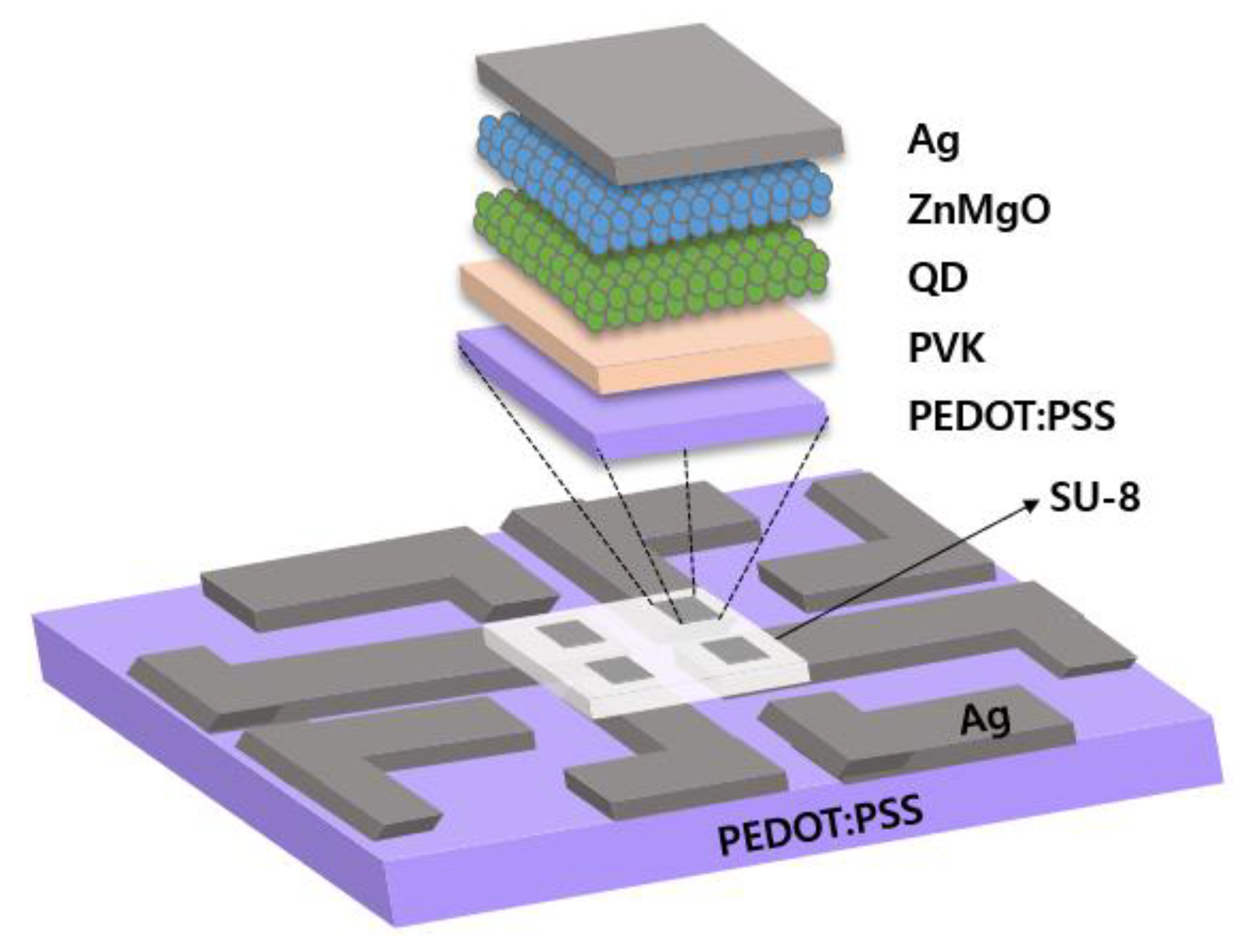
This paper presents the development of highly efficient TE-QLEDs achieved by adjusting the thickness of the ZnMgO NP ETL, resulting in modifications that include variations in conductivity due to changes in oxygen vacancy concentration, and alterations in quenching sites influenced by changes in hydroxyl (-OH) species concentration. By employing X-ray photoelectron spectroscopy (XPS) measurement, the study examined the concentration of oxygen vacancy and the concentration of hydroxyl species. This analysis aimed to understand electron injection and electron transport mechanism in the ZnMgO ETL, as well as non-radiation recombination at the QD-ZnMgO interface. As a result, the presented TE-QLED with a 30-nm-thick Zn0.9Mg0.1O NP ETL demonstrated outstanding performance, achieving a maximum current efficiency of 91.92 cd/A and a maximum EQE of 21.66%. We believe that employing Zn0.9Mg0.1O NP ETL with an appropriate thickness holds promise for achieving high-performance TE-QLEDs suitable for next-generation displays and lighting applications.
3. Results and Discussion
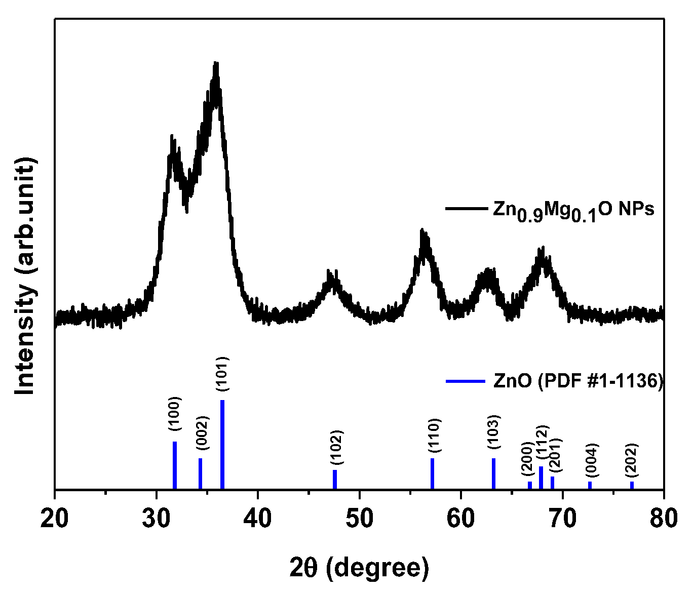
Figure 2 illustrates the characteristic X-ray diffraction (XRD) pattern of the Zn
0.9Mg
0.1O NPs obtained by scanning the 2θ range. The XRD pattern was analyzed to investigate the crystal structure and crystallite size of Zn
0.9Mg
0.1O NPs. It reveals a hexagonal wurtzite structure, which is characteristic feature of ZnO, as confirmed by comparing it to the Joint Committee on Powder Diffraction Standards (JCPDS Card No. 1-1136). The XRD pattern of Zn
0.9Mg
0.1O NPs exhibits reflections in the (100), (002), (101), (102), (110), (103) and (112) planes, all of which are attributable to the ZnO phase. A slight shift in the diffraction peak and intensity of the Zn
0.9Mg
0.1O NPs is observed, suggesting a minor lattice distortion and altered interatomic spacing.
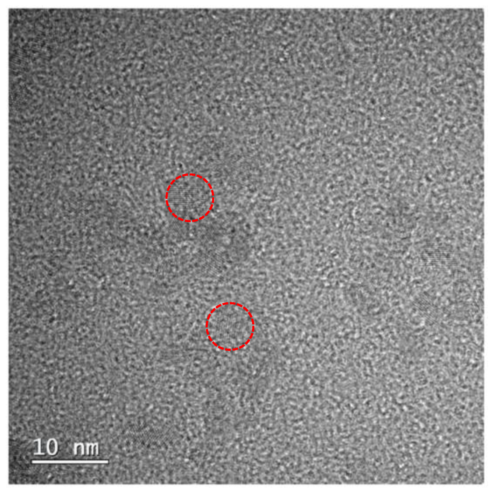
Figure 3 presents a typical field-emission transmission electron microscopy (FE-TEM) image of the Zn
0.9Mg
0.1O NPs. The size of the Zn
0.9Mg
0.1O NPs was determined through FE-TEM analysis, revealing an average diameter of 4.61 nm.
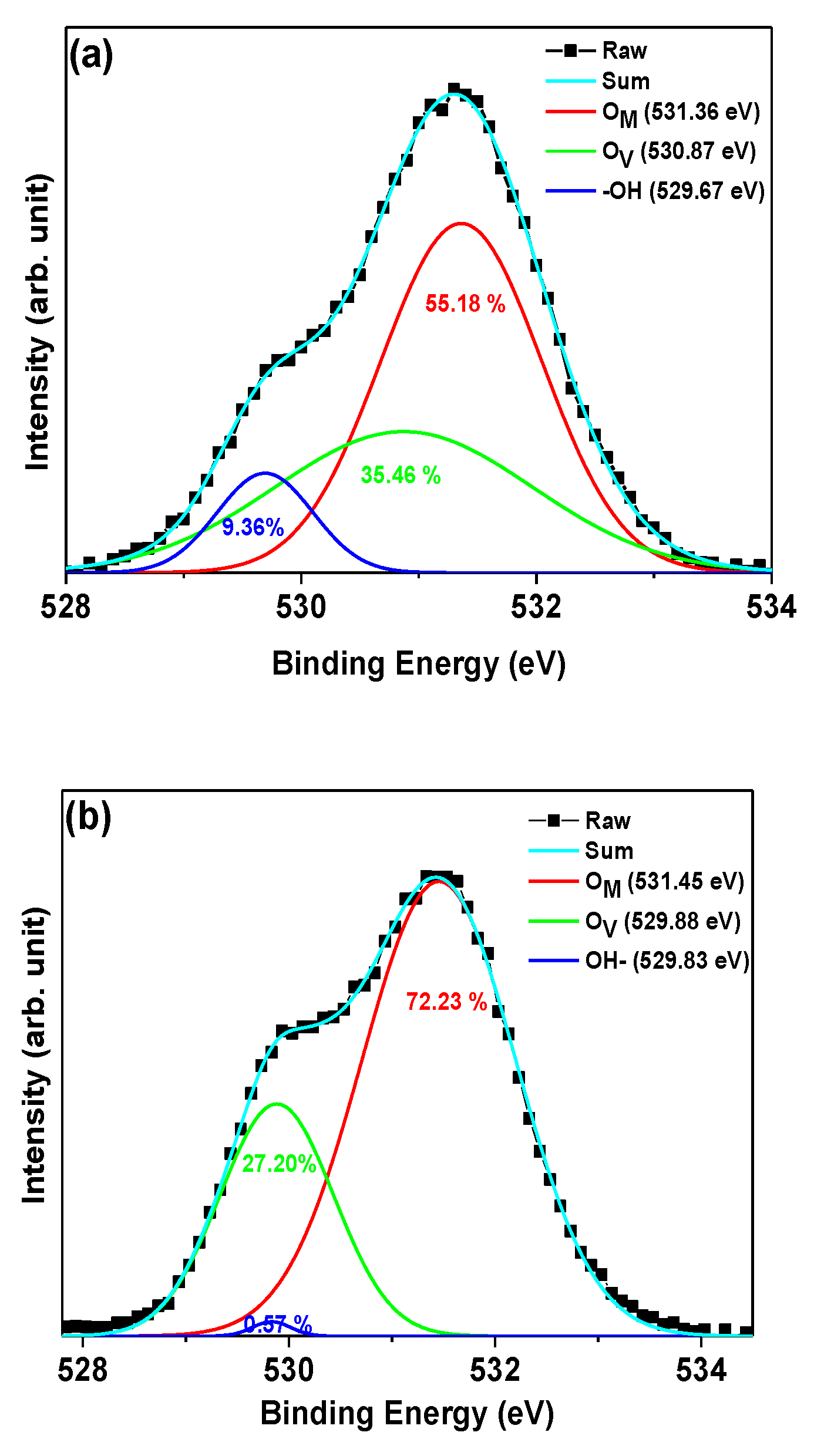
XPS measurements were conducted to examine the oxygen configuration of Zn
0.9Mg
0.1O NP thin film as a function of varying thickness, providing information about the quality of the NPs, as shown in
Figure 4. This figure illustrates the normalized O 1s spectra of the Zn
0.9Mg
0.1O NPs deposited onto the PEDOT:PSS (25 nm)/Ag (150 nm)/PEDOT:PSS (25 nm)/QD (10 nm) substrate. By employing deconvolution, three peaks were extracted, each corresponding to specific components, including the metal oxide lattice bond (O
M), oxygen vacancies O
2- ions (O
V), and hydroxyl (O
OH) species. [
33]. The area of each peak exhibited variations depending on the thickness of the Zn
0.9Mg
0.1O NP thin film [34-36]. O
T represents the overall O 1s peak.
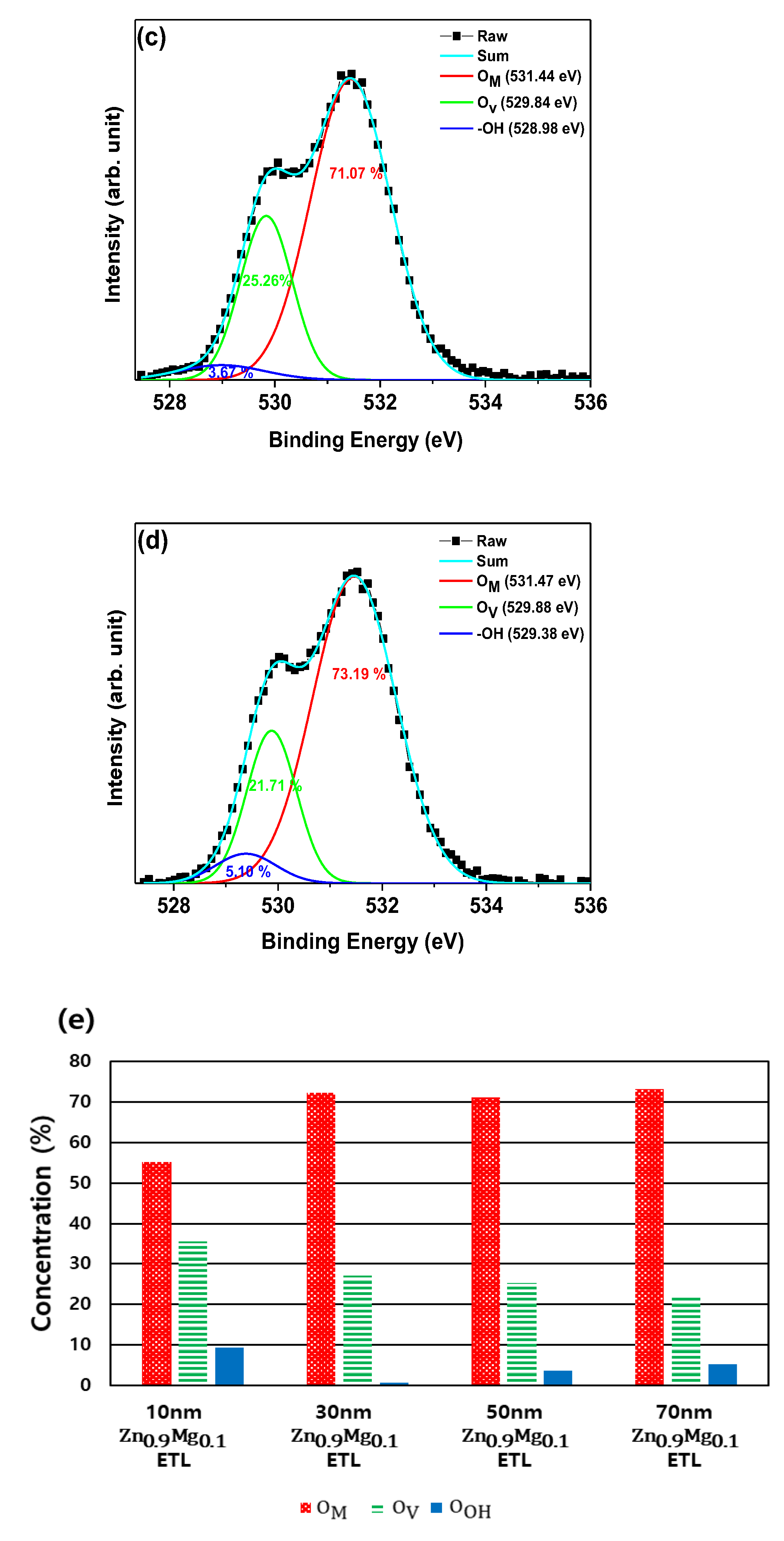
Figure 4(e) includes a distribution graph illustrating the ratio of the areas of the three peaks areas concerning the thickness of Zn
0.9Mg
0.1O NP thin film. The ratios of the peak area (O
V/O
T) of 10-nm-thick Zn
0.9Mg
0.1O NP thin film, 30-nm-thick Zn
0.9Mg
0.1O NP thin film, 50-nm-thick Zn
0.9Mg
0.1O NP thin film, and 70-nm-thick Zn
0.9Mg
0.1O NP thin film were calculated to be 35.46%, 27.20%, 25.26%, and 21.70%, respectively. On the other hand, the ratios of the peak area (O
OH/O
T) of 10-nm-thick Zn
0.9Mg
0.1O NP thin film, 30-nm-thick Zn
0.9Mg
0.1O NP thin film, 50-nm-thick Zn
0.9Mg
0.1O NP thin film, and 70-nm-thick Zn
0.9Mg
0.1O NP thin film were estimated to be 9.36%, 0.57%, 3.67%, and 5.10%, respectively. With an increase in thickness, there was a noticeable trend towards a higher concentration of metal oxide lattice bonds, while the concentration of the oxygen vacancies decreased. The oxygen vacancies act as trap sites, and an increase in these sites leads to higher carrier concentration, enhanced conductivity, and reduced resistance of the Zn
0.9Mg
0.1O NP thin film [
37]. Furthermore, the XPS results indicate that the Zn
0.9Mg
0.1O NP thin film with a thickness of 30 nm exhibits the lowest concentration of hydroxyl species. A reduction in the hydroxyl species within the Zn
0.9Mg
0.1O NP thin film resulted in reduced quenching effects at interface, thereby extending the lifetime of QDs [
38]. Based on these results, it can be expected that TE-QLEDs with a 30-nm-thick Zn
0.9Mg
0.1O NP ETL will demonstrate high luminance and EQE.
Figure 3.
Field-emission transmission electron microscopy of Zn0.9Mg0.1O NPs.
Figure 3.
Field-emission transmission electron microscopy of Zn0.9Mg0.1O NPs.
To investigate the influence of the bank enclosure on leakage current, electroluminescent characteristics were examined.
Figure S1(a) depicts the current density versus applied voltage curves of TE-QLED with a 50-nm-thick Zn
0.9Mg
0.1O NP ETL with a 50-nm-thick Zn
0.9Mg
0.1O NP ETL, both fabricated inside and without the bank enclosure. It is noteworthy that when voltages of up to 8 V were applied, the TE-QLED with a 50-nm-thick Zn
0.9Mg
0.1O NP ETL fabricated without the bank enclosure exhibited a higher leakage current, characterized by a raised, and rounded peak. In contrast, the TE-QLED with a 50-nm-thick Zn
0.9Mg
0.1O NP ETL fabricated inside the bank enclosure did not exhibit such a raised and rounded peak and had a much lower leakage current. Additionally, throughout the entire measurement range, the current density of the TE-QLED with a 50-nm-thick Zn
0.9Mg
0.1O NP ETL fabricated without the bank enclosure was higher than that of the TE-QLED with a 50-nm-thick Zn
0.9Mg
0.1O NP ETL fabricated inside the bank enclosure, likely due to leakage current.
Figure 4.
X-ray photoelectron spectroscopy O 1s spectra of Zn0.9Mg0.1O NP thin films with varying thickness deposited onto a PEDOT:PSS/Ag/PEDOT:PSS/PVK/QD substrate: (a) 10-nm-thick Zn0.9Mg0.1O NP thin films, (b) 30-nm-thick Zn0.9Mg0.1O NP thin films, (c) 50-nm-thick Zn0.9Mg0.1O NP thin films, (d) 70-nm-thick Zn0.9Mg0.1O NP thin films. (e) Area ratio of each of the three peaks in relation to the change in thickness of Zn0.9Mg0.1O NP thin films. .
Figure S1(b) illustrates that the turn-on volage at 1 cd/m
2 of the TE-QLED with a 50-nm-thick Zn
0.9Mg
0.1O NP ETL fabricated inside the bank enclosure was lower than that of the TE-QLED with a 50-nm-thick Zn
0.9Mg
0.1O NP ETL fabricated without the bank enclosure. Additionally, in the low voltage range, the TE-QLED with a 50-nm-thick Zn
0.9Mg
0.1O NP ETL fabricated inside the bank enclosure exhibited higher luminance compared to the TE-QLED with a 50-nm-thick Zn
0.9Mg
0.1O NP ETL fabricated without the bank enclosure. This suggests that the charge balance between electrons and holes within the EML of the TE-QLED with a 50-nm-thick Zn
0.9Mg
0.1O NP ETL fabricated inside the bank enclosure was better achieved in the low voltage range. However, in the high voltage range, the TE-QLED with a 50-nm-thick Zn
0.9Mg
0.1O NP ETL fabricated inside the bank enclosure exhibited lower luminance than the TE-QLED with a 50-nm-thick Zn
0.9Mg
0.1O NP ETL fabricated without the bank enclosure. This indicates that in the high voltage range, the charge balance between electrons and holes within the EML of the TE-QLED with a 50-nm-thick Zn
0.9Mg
0.1O NP ETL fabricated inside the bank was not as effectively achieved as in the counterpart without bank enclosure, leading to an observed roll-off in the current efficiency in the TE-QLED with a 50-nm-thick Zn
0.9Mg
0.1O NP ETL fabricated inside the bank enclosure.
Figure S1(c) presents the current efficiency versus applied voltage curves of TE-QLEDs with a 50-nm-thick Zn
0.9Mg
0.1O NP ETL, both fabricated inside and without the bank enclosure. It is evident that the TE-QLED with a 50-nm-thick Zn
0.9Mg
0.1O NP ETL fabricated inside the bank enclosure achieved a higher maximum current efficiency compared to its counterpart fabricated without the bank enclosure. This improvement can be attributed to the bank enclosure’s role in constraining leakage current.
Figure S1(d) illustrates the electroluminescence (EL) spectra of the TE-QLEDs with a 50-nm-thick Zn
0.9Mg
0.1O NP ETL, both fabricated inside and without the bank enclosure. Both TE-QLEDs have their peak values centered at 524 nm. However, the full width at half maximum (FWHM) of the TE-QLED fabricated inside the bank enclosure is narrower than that of the TE-QLED fabricated without the bank enclosure. This indicates that the charge balance in the EML of the TE-QLED fabricated inside the bank enclosure is better achieved than in the TE-QLED fabricated without the bank.
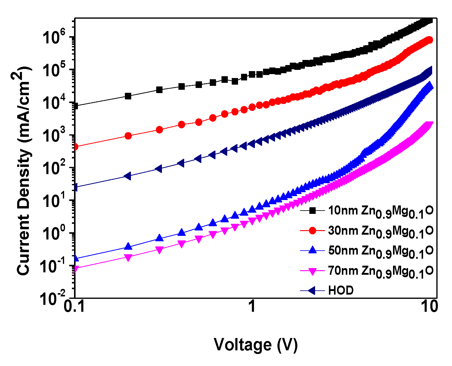
Figure 5.
Current density versus applied voltage of the electron-only devices (EODs) according to various thickness of Zn0.9Mg0.1O NPs (10 nm, 30 nm, 50 nm, and 70 nm), and the hole-only device (HOD).
Figure 5.
Current density versus applied voltage of the electron-only devices (EODs) according to various thickness of Zn0.9Mg0.1O NPs (10 nm, 30 nm, 50 nm, and 70 nm), and the hole-only device (HOD).
Electron-only devices (EODs) and hole-only devices (HOD) were fabricated to investigate the hole and electron injection, as well as electron transport behaviors. Four different EODs were developed, each with varying Zn
0.9Mg
0.1O NPs thickness (10 nm, 30 nm, 50 nm, and 70 nm), as illustrated in
Figure 6. Additionally, a HOD was also created. The EOD structures consisted of Ag (150 nm)/Zn
0.9Mg
0.1O NPs (10 nm, 30 nm, 50 nm, 70 nm)/QD (10 nm)/Zn
0.9Mg
0.1O NPs (10 nm, 30 nm, 50 nm, 70 nm)/Ag (150 nm), while the HOD structure was Ag (150 nm)/PEDOT:PSS (25 nm)//PVK (40 nm)/QD (10 nm)/Ag (150 nm). The thickness of the Zn
0.9Mg
0.1O NPs on both sides of the QDs for EODs was the same. The additional layer of Zn
0.9Mg
0.1O NPs on the anode side was added to block incoming holes from the anode and prevent excessive current flow through the device. Electrons can be injected from the cathode to the conduction band minimum (CBM) level of QDs via the CBM level of ZnMgO NPs. The measurements from EODs revealed that as the thickness of the Zn
0.9Mg
0.1O NPs increased, the current density of EODs decreased. This observation is consistent with the XPS results, which show a reduction in oxygen vacancy as the thickness of Zn
0.9Mg
0.1O NPs increases. This leads to decreased conductivity and an increase in resistance of the Zn
0.9Mg
0.1O NP ETL. Furthermore, an increase in thickness of the Zn
0.9Mg
0.1O NP ETL leads to higher resistance. The current density obtained from HOD fell within the range of the current densities obtained from EODs with thickness of 30 nm and 50 nm. This implies that optimal charge balance in the QD EML can be achieved in the TE-QLED when using either a 30 nm or 50 nm thickness of ZnMgO as the ETL.
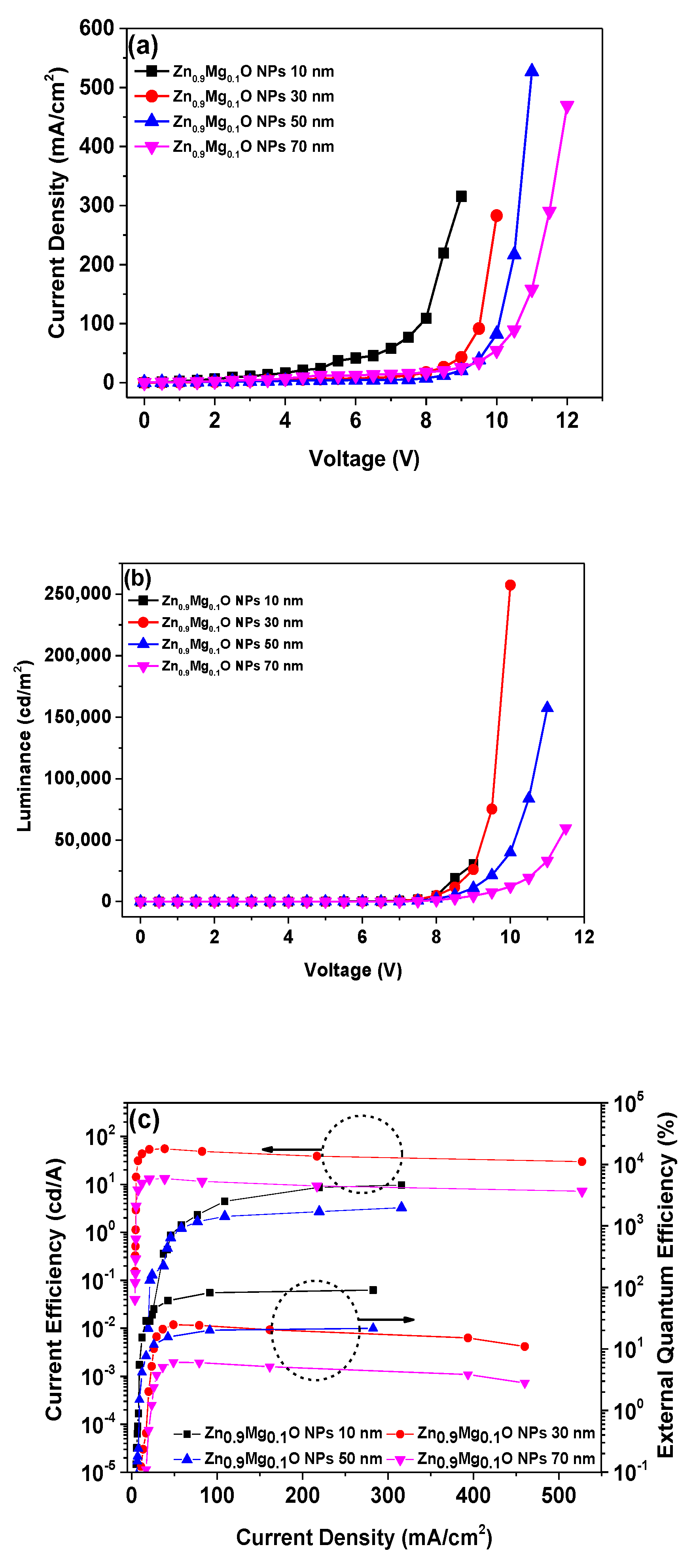
Figure 6 illustrates the EL characteristics of the TE-QLEDs employing Zn
0.9Mg
0.1O NP ETLs with varying thicknesses: 10 nm, 30 nm, 50 nm, and 70 nm. In
Figure 6(a), the curves for current density and luminance are presented as functions of applied voltage. It is noteworthy that as the thickness of the Zn
0.9Mg
0.1O NP ETL increases, there is a notable decrease in current density. This phenomenon can be attributed to a reduction in conductivity resulting from a decreased concentration of oxygen vacancies within the Zn
0.9Mg
0.1O NP ETL, as supported by XPS results. Furthermore, this decrease in current density can also be linked to the decreased electric field, resulting from the increased thickness of the ETL.
Figure 6.
Electroluminescence (EL) characteristics of the TE-QLEDs utilizing Zn0.9Mg0.1O NP ETLs with different thicknesses: 10 nm, 30 nm, 50 nm, and 70 nm: (a) Current density-voltage curves as a function of voltage, (b) luminance curves as a function of current density, and (c) current efficiency and external quantum efficiency curves as a function of current efficiency. .
The turn-on voltages at 1 cd/m
2 for the TE-QLEDs with 10-nm-thick, 30-nm-thick, 50-nm-thick, and 70-nm-thick Zn
0.9Mg
0.1O NP ETLs were extrapolated to be 4.15 V, 4.06 V, 4.57 V, 4.65 V, and 4.52 V, respectively. This indicates that the TE-QLED with a 30-nm-thick Zn
0.9Mg
0.1O NP ETL exhibited the lowest turn-on voltage, indicating minimized exciton quenching at the interface between the QD and Zn
0.9Mg
0.1O NP ETL. This reduction can be attributed to a decrease in hydroxyl species, as confirmed by XPS analysis, and the achievement of optimal charge balance in the QD EML. Additionally,
Figure 6(a) illustrates the maximum luminance values of TE-QLEDs with 10-nm-thick, 30-nm-thick, 50-nm-thick, and 70-nm-thick Zn
0.9Mg
0.1O NP ETLs, estimated at 30,560.1 cd/m
2, 257,307.4 cd/m
2, 157,337.4 cd/m
2, and 59,782.06 cd/m
2, respectively. The TE-QLED with a 30-nm-thick ZnMgO NP ETL exhibited the highest luminance among the four TE-QLEDs with varying Zn
0.9Mg
0.1O NP ETL thicknesses. This observation was confirmed by analysis of EODs and HOD, as shown in
Figure 3, suggesting that a balanced charge distribution between electrons and holes within the QD EML was likely more effectively achieved in the TE-QLED with a 30-nm-thick ZnMgO NP ETL or the one with a 50-nm-thick ZnMgO NP ETL. Moreover, it is believed that the lower concentration of hydroxyl species in the ZnMgO NPs, as observed in the XPS analysis depicted in
Figure 4, minimized exciton quenching at the interface between QD EML and Zn
0.9Mg
0.1O NP ETL, resulting in higher luminance.
Figure 6(c) presents the current efficiencies and EQE of the TE-QLEDs employing Zn
0.9Mg
0.1O NP ETLs with different thicknesses: 10 nm, 30 nm, 50 nm, and 70 nm. The maximum current efficiencies of TE-QLEDs with 10-nm-thick, 30-nm-thick, 50-nm-thick, and 70-nm-thick Zn
0.9Mg
0.1O NP ETLs were measured at be 9.68 cd/A, 90.92 cd/A, 55.33 cd/A, and 20.98 cd/A, respectively. Simultaneously, the maximum EQEs for TE-QLEDs with 10-nm-thick, 30-nm-thick, 50-nm-thick, and 70-nm-thick Zn
0.9Mg
0.1O NP ETLs were estimated to be 3.28%, 21.66%, 13.22%, and 6.08%, respectively. Remarkably, the TE-QLED with a 30-nm-thick Zn
0.9Mg
0.1O NP ETL exhibited an outstanding maximum current efficiency and maximum EQE of 90.92 cd/A and 21.66%, respectively. These results align with our earlier discussion, underscoring the significance of choosing the right Zn
0.9Mg
0.1O NP ETL thickness to achieve charge balance and minimize the concentration of hydroxyl species acting as quenching sites at the interface between QD EML and Zn
0.9Mg
0.1O NP ETL at that thickness.
Table 1 summarizes the key parameters obtained from the TE-QLEDs employing Zn
0.9Mg
0.1O NP ETLs with varying thicknesses: 10 nm, 30 nm, 50 nm, and 70 nm.
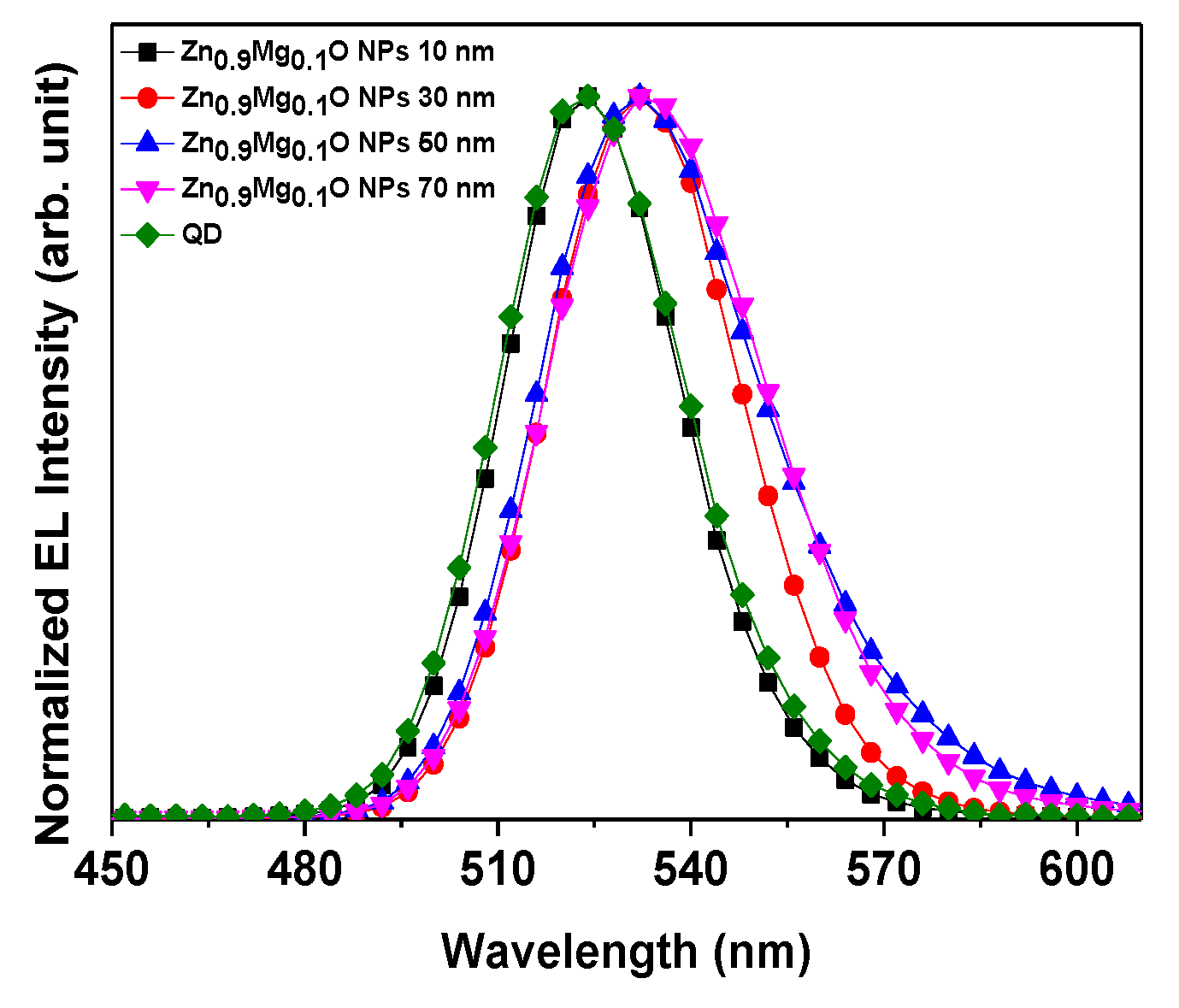
Figure 7 illustrates the normalized photoluminescence (PL) spectrum of the CdSe/ZnS QD, along with EL spectra from the TE-QLEDs employing Zn
0.9Mg
0.1O NP ETLs with various thicknesses: 10 nm, 30 nm, 50 nm, and 70 nm. A summary of the characteristic parameters for these spectra is provided in
Table 2. The EL peak of the TE-QLED with a 10-nm-thick Zn
0.9Mg
0.1O NP ETL is centered at 524 nm, matching the PL peak of the CdSe/ZnS QD. In contrast, the EL peaks of TE-QLEDs with 30-nm thick, 50-nm-thick, and 70-nm-thick Zn
0.9Mg
0.1O NP ETLs are centered at 532 nm, indicating a red-shift compared to the PL peak of the CdSe/ZnS QD. These red shifts can be attributed to factors such as Föster energy transfer, dielectric dispersions, and the Stark effect occurring under high voltage and current conditions [
39,
40]. Furthermore, Figure 8 also demonstrates that the spectra’s FWHM increases as the thickness of the Zn
0.9Mg
0.1O NP ETLs increases. However, when the thickness of the Zn
0.9Mg
0.1O NP ETL is 10 nm, it is considered too thin to have a significant impact. The TE-QLED with a 30-nm-thick Zn
0.9Mg
0.1O NP ETL exhibited the narrowest FWHM of 328 nm, indicating that the best charge balance occurred in the QD EML. The absence of parasitic PVK emission confirms that the device emission primarily results from electron-hole recombination within the CdSe/ZnS QD EML. These findings can be attributed to the effective charge balance achieved between holes and electrons within the e CdSe/ZnS QD EML
Table 1.
The performance parameters of TE-QLEDs with various thickness of Zn0.9Mg0.1O NPs.
Table 1.
The performance parameters of TE-QLEDs with various thickness of Zn0.9Mg0.1O NPs.
Thickness of
Zn0.9Mg0.1O NP ETL
(nm) |
Turn-on voltage
at Current Density
(V) |
Turn-on voltage at 1 cd/m2
(V) |
Current Density at 9 V
(mA/cm2) |
Maximum Luminance
(cd/m2) |
Maximum
Current Efficiency
(cd/A) |
Maximum EQE
(%) |
| 10 |
0.49 |
4.15 |
315.75 |
30560.06 |
9.68 |
3.28 |
| 30 |
1.51 |
4.06 |
42.75 |
257307.4 |
90.92 |
21.66 |
| 50 |
0.99 |
4.57 |
20.75 |
157337.4 |
55.33 |
13.22 |
| 70 |
0.99 |
4.65 |
25.75 |
59782.06 |
20.98 |
6.08 |
