Submitted:
09 November 2023
Posted:
13 November 2023
You are already at the latest version
Abstract
Keywords:
Introduction
Liquid crystal circular devices
II.1. Liquid crystal lenses
II.1.1. Graded index lenses
II.1.2. Designing LC lenses
- Zonal or pixelated lenses generate the quadratic index profile through independent electrodes. SLMs can be used to make such lenses; however, it is usual to employ pixels shaped as concentric rings [27].
- Modal lenses are able to produce smooth profiles without pixelization, just one continuous electrode or a few of them at most. The electric field distribution –hence the index profile– is achieved employing high resistivity electrodes, usually between 100’s o and some o. High resistivity electrodes can be made of several materials, such as PEDOT-PSS [28] or ultrathin ITO [29].
- The high resistivity electrode behaves as a transmission line [30] profile can be modified varying the voltage amplitude and the frequency; thereby making it possible to create radial voltage gradients that follow up the required quadratic index profiles for lenses, or other profiles for different optical elements e.g., axicons. Modal control has been also proposed in Fresnel lens [31], that will be commented below.
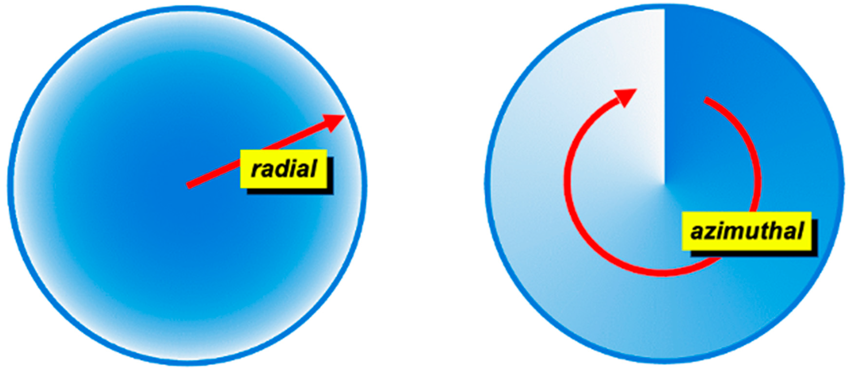
- rather different approach is given by Pancharatnam-Berry phase devices (PPD, [35]), and specifically Pancharatnam-Berry lenses. PPDs are elements in which electromagnetic waves undergo continuous phase changes due to a continuous change in the material through which they are passing. Typically, liquid crystal PPDs work by smooth variations of the alignment directions on both confining surfaces of a retardation liquid crystal cell, i.e., introducing a fixed linear retardation with variable azimuthal angle.
- Such a PPD inverts the handedness of incident circularly polarized light and introduces a relative phase delay depending on the local alignment direction of the waveplate, as will be discussed below. These devices and lenses have a wide range of applications with a spatial phase variation pitch beyond anything achievable in conventional SLMs or ITO based devices [36,37].
- However, unless special effort is invested, the devices will have opposite behavior for the two handedness of circularly polarized light, which makes them “unstackable”, and typically only provide an ON-OFF switching behavior optimized for a single wavelength. Thus, the main drawbacks of PPDs are their deficient tunability and their strong dependence on the wavelength of impinging light [38].
II.1.3. Increasing LC lens power
- Use high birefringence LCs [42]. This can be helpful, but it is not a solution by itself. At present, high BR mixtures are in the range 0.4 – 0.5, which would double or triple the lens power at most.
- Increase cell thickness. LC cell thicknesses above 100 µm driven by ultrasounds have been proposed [43]. For electrically driven cells, however, thickness is severely restricted –usually to 20-30 µm– by response time degradation and poor material orientation in thick cells. Again, alternative solutions including dual frequency nematics [44] and polymerization [45] have been proposed, so that the spatial orientation of LC molecules is kept, and the response time is improved.
- Decrease the cell radius. This would alleviate the strong dependence that thwarts the lens power. A diopters lens of 1 cm diameter like the above glass lens would require an LC thickness of 314 µm, impossible to control or orient with standard fabrication procedures. (Not surprisingly, this is the thickness difference required for the glass lens, were its refractive index 1.2 rather than 1.5, i.e., .) If the LC lens diameter is set to 2 mm, then the required LC thickness is 12.5 µm, a perfectly feasible value. Many groups work on LC microlens arrays [46,47] to take advantage of small diameters while keeping reasonable apertures.
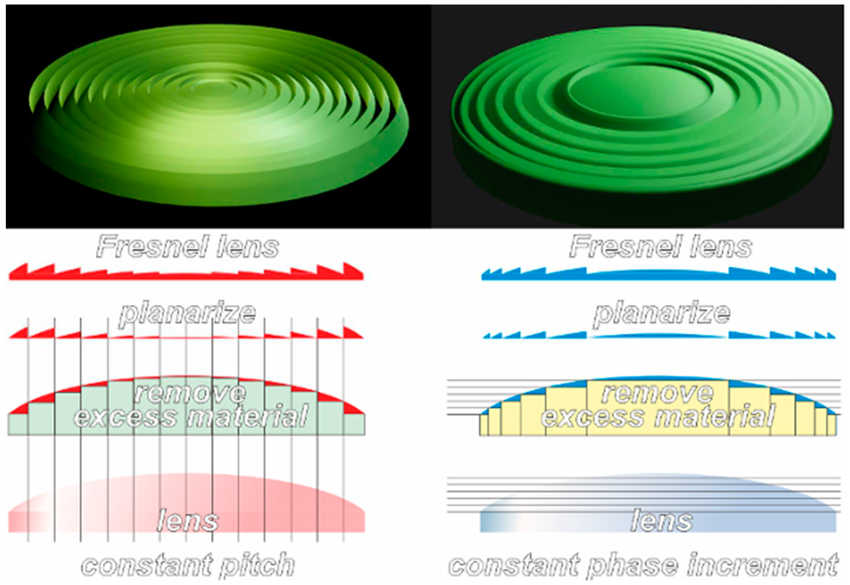
- Create Fresnel lenses. Fresnel geometry provides the most powerful solution, capable of producing high-power, high aperture lenses [48] with outstanding fill factor and excellent time response. This topic is dealt in next sections.
II.2. Fresnel lenses
II.2.1. Types of Fresnel lenses
II.2.2. LC Fresnel lenses
II.3. Axicons
II.4. Vortices
II.4.1. Orbital angular momentum and topological charge
II.4.2. Liquid crystal vortices
II.4.3. Perfect Vortex Beams
II.5. Q-plates
II.5.1. Halfwave retardations on circular light
II.5.2. PPDs and Q-plates
II.5.3. Limitations of Q-plates
Polarization-independent devices: Blue Phases
III.1. Orientation of BPs
III.1.1. Kossel patterns
III.1.2. Conventional alignment
III.1.3. Advanced alignments
III.2. Thermal stabilization
III.3. Applications of BPs
Spirals
IV.1. Geometrical spirals
IV.2. Experimental implementations
IV.2.1. Interleaving
IV.2.2. Electrical connections
IV.3. Spirals as alternative approach
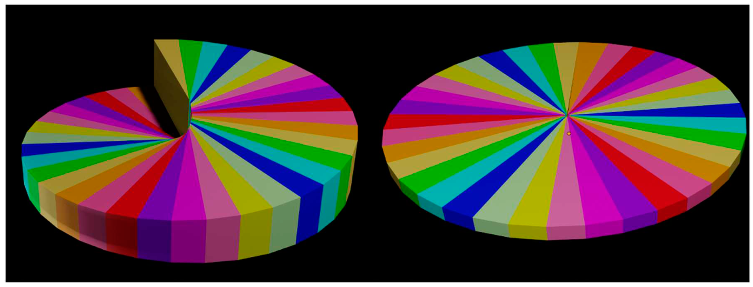
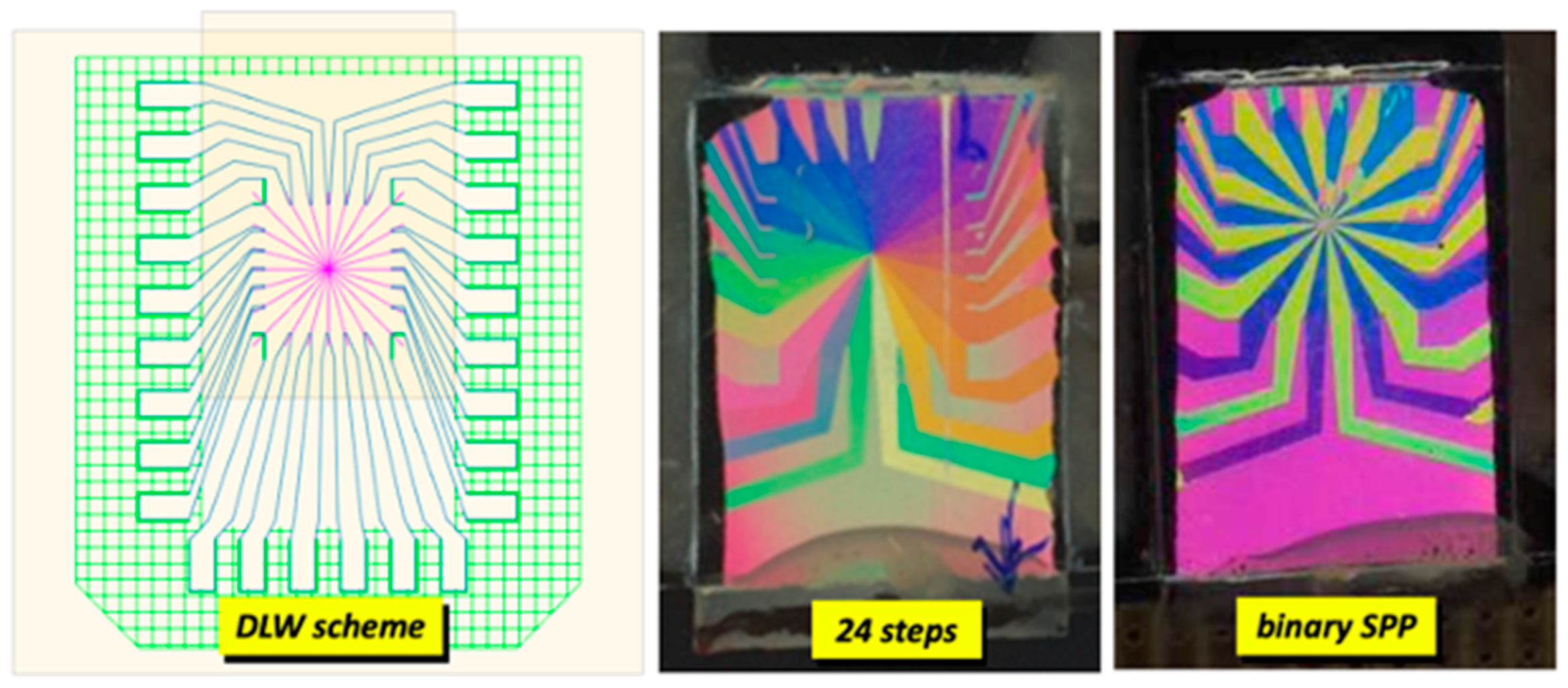
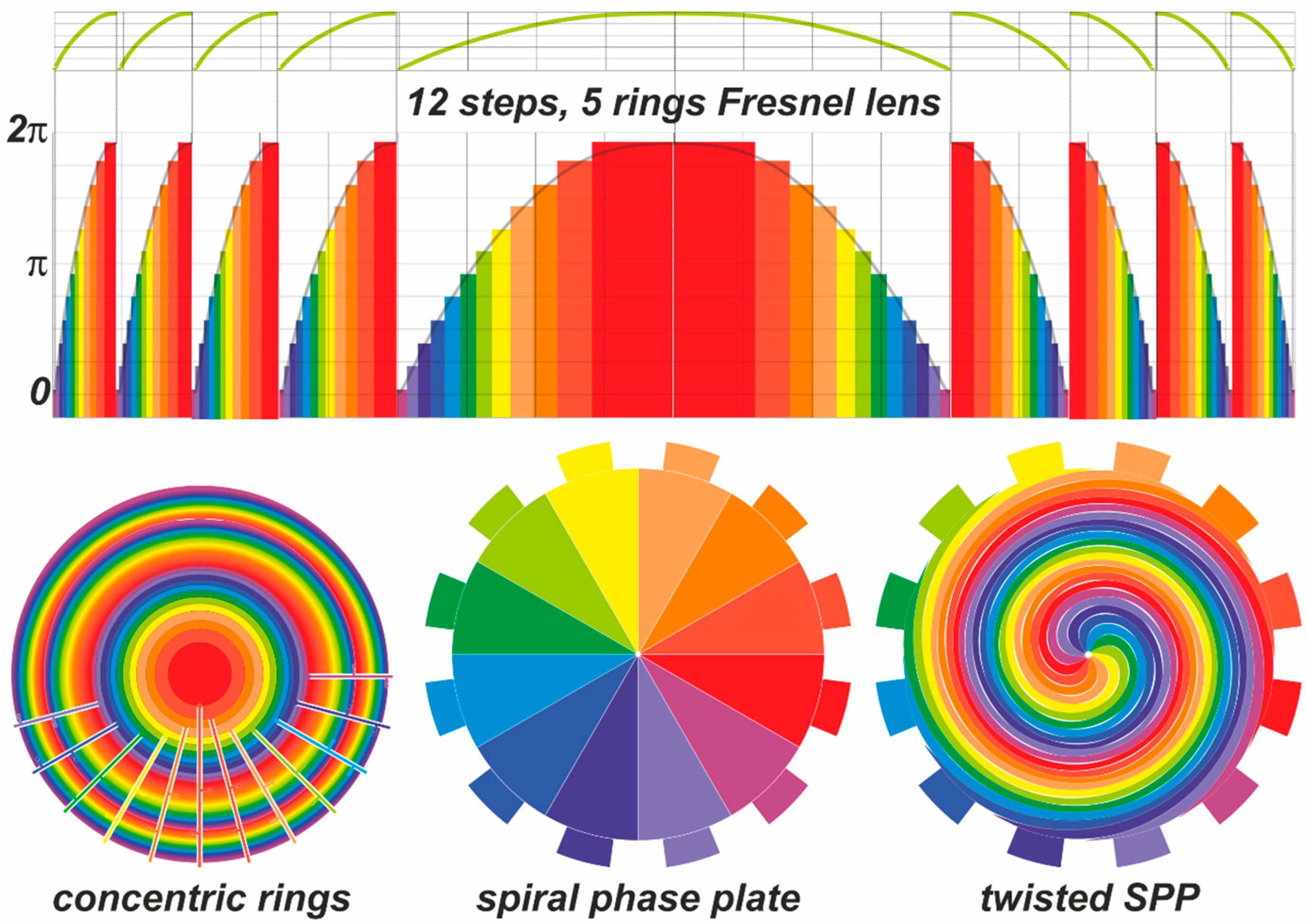
- Design a 12-pie slice spiral phase plate (Figure 19, bottom center) with external electric connections.
- Twist the SPP five turns.
IV.3.1. Design of spiral lenses and axicons
IV.3.2. Fill factor
IV.4. Tunability of spiral lenses
IV.4.1. Assembling spiral lenses
IV.4.2. Tunable SDLs
IV.4.2. Analog vs. Digital SDLs
IV.4.3. Obtaining true Fresnel lenses
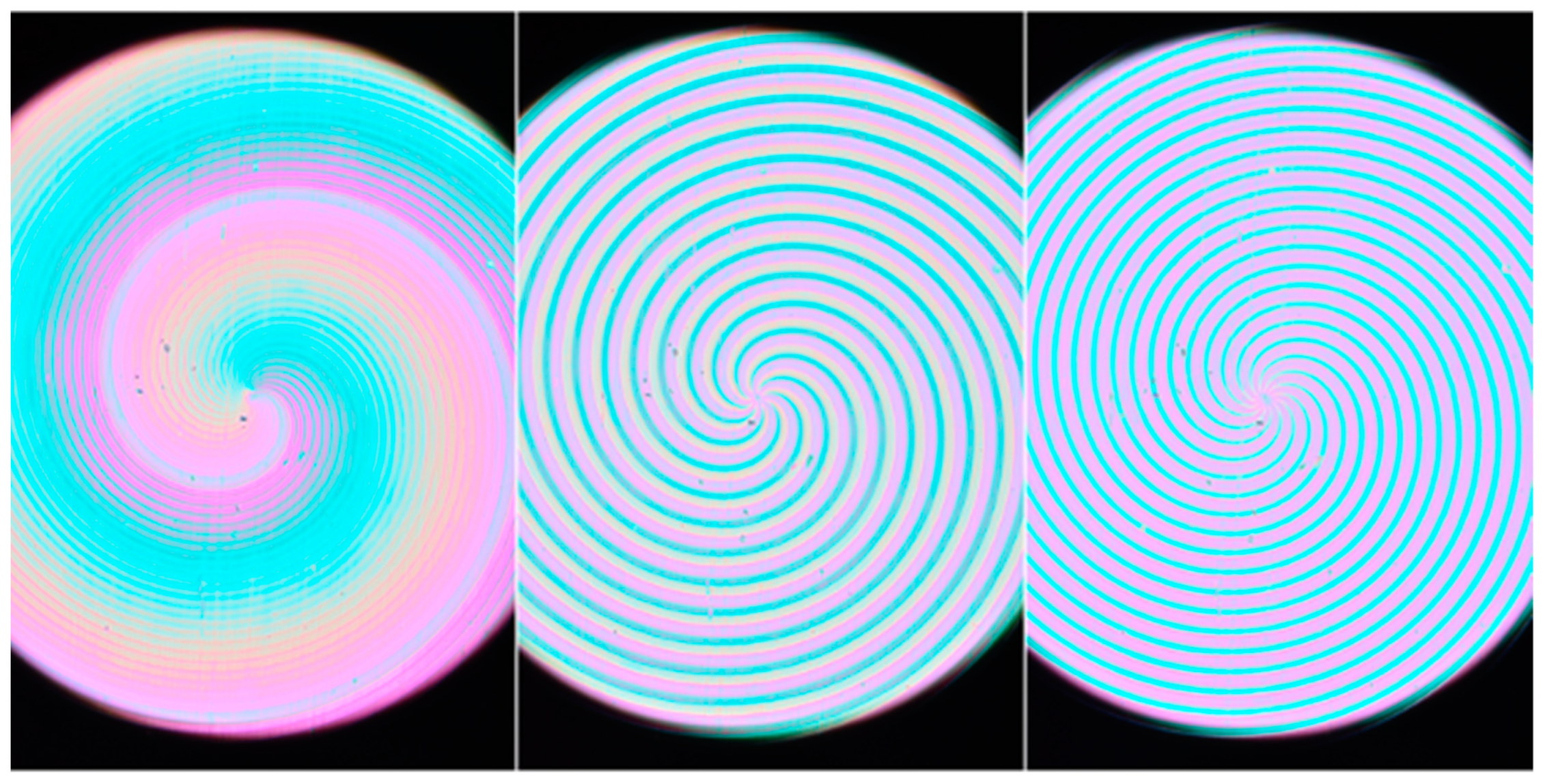
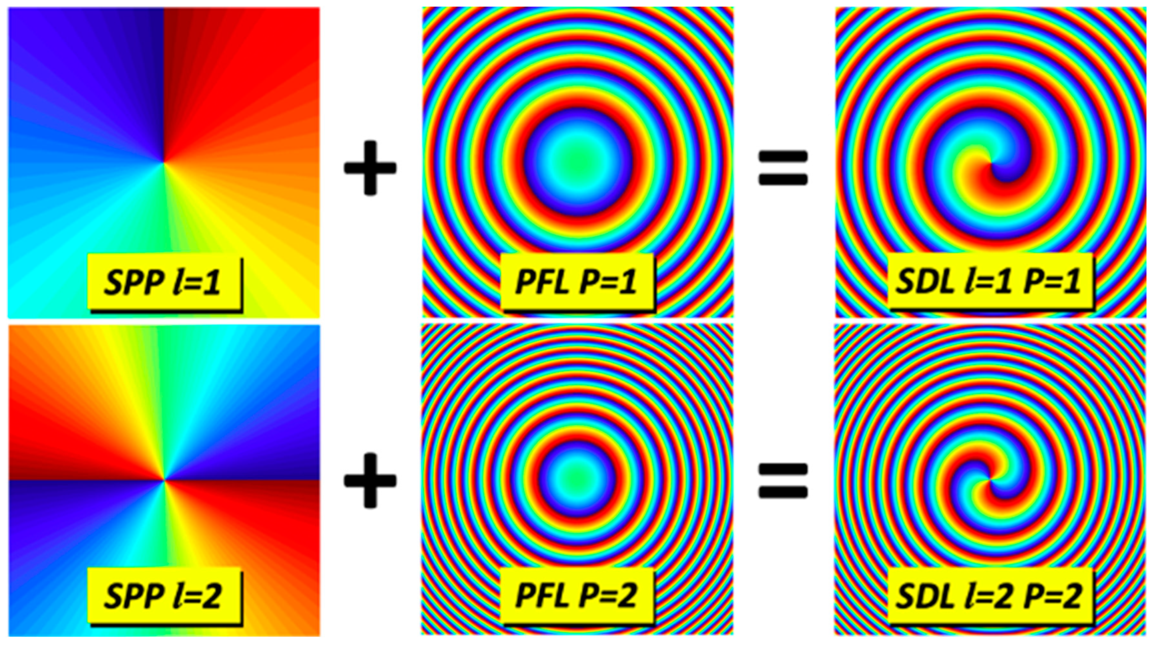
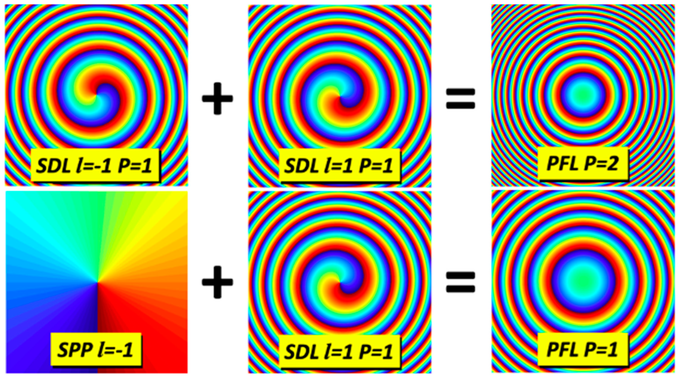
- By superimposing on the SDL an SPP with the same topological charge but opposite sign, the topological charges cancel out and the result is equivalent to a classical Fresnel lens of the same power.
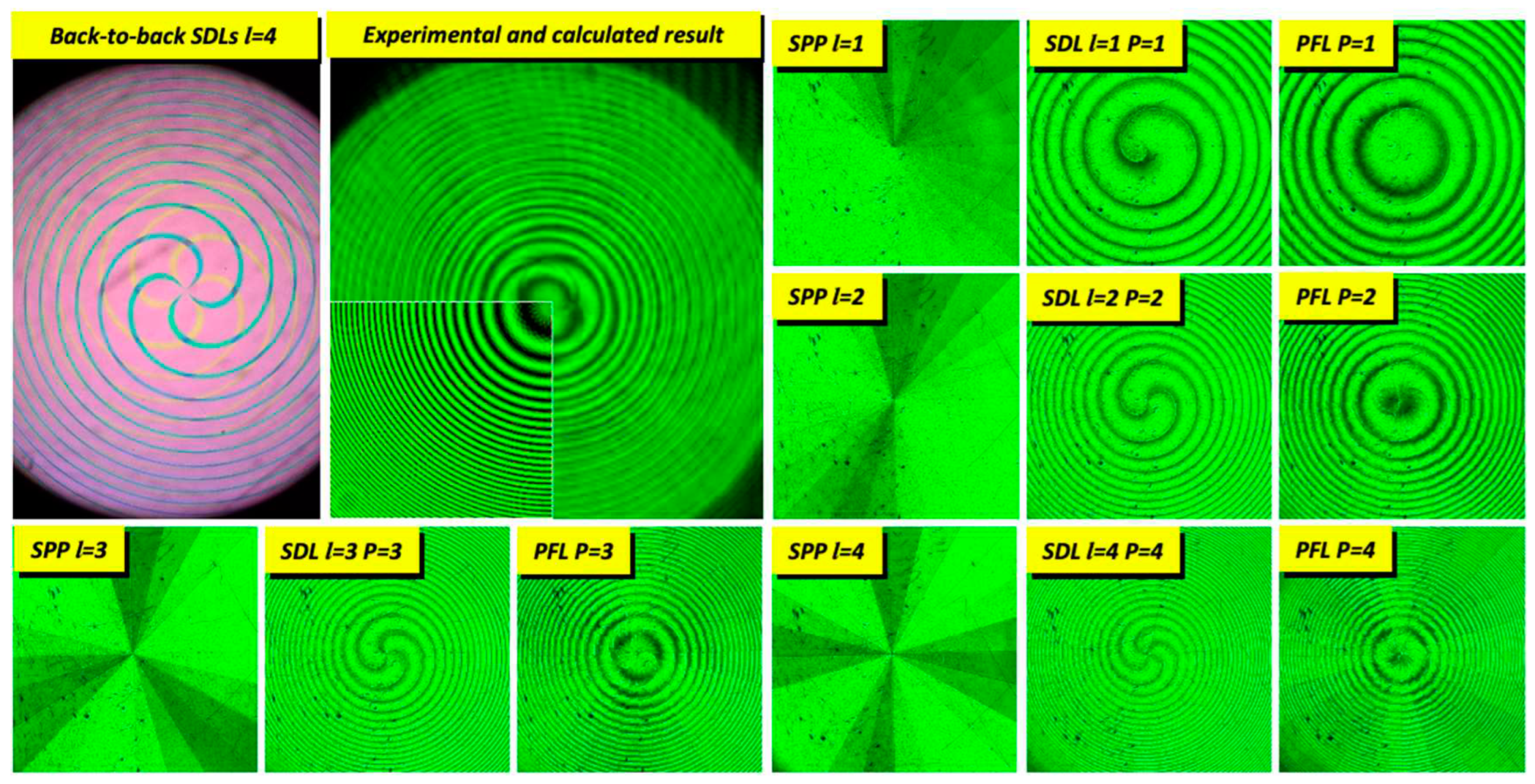
- The topological charge can also be canceled by using two identical lenses with inverse topological charge. It is achieved building a device made up of two units of the same lens coupled back-to-back. The topological cancellation is identical to the previous case, but the power of the resulting lens is twice the power of the individual lenses.
IV.4.4. Experimental verification
Conclusions
References
- Ajay Singh “Liquid Crystal Spatial Light Modulators” https://www.slideshare.net/azadajay/liquid-crystal-slms (downloaded May 2023).
- Cátia Pinho, Isiaka Alimi, Mário Lima, Paulo Monteiro, António Teixeira “Spatial Light Modulation as a Flexible Platform for Optical Systems” in “Telecommunications Systems – Principles and Applications of Wireless-Optical Technologies” Isiaka A. Alimi, Paulo P. Monteiro and António L. Teixeira eds., IntechOpen, ISBN 978-1-78984-294-4 (2021). [CrossRef]
- Andrei Drāgulinescu “Optical Correlators for Cryptosystems and Image Recognition: A Review” Sensors 23 (2) 907 (2023). [CrossRef]
- Hsi-Hsir Chou, Chia-Lun Chen “Asymmetric Optical Wavelength Switch based on LCoS-SLM for Edge Node of Optical Access Network” IEEE Photon. J. 13 (4) 1 (2021). [CrossRef]
- Yiran Ma, Luke Stewart, Julian Armstrong, Ian G. Clarke, Glenn Baxter “Recent Progress of Wave length Selective Switch” J. Lightwave Technol. 39 (4) 896 (2021). [CrossRef]
- Byounghyo Lee, Dongyeon Kim, Seungjae Lee, Chun Chen, Byoungho Lee “High-contrast, speckle-free, true 3D holography via binary CGH optimization” Sci. Rep. 12, 2811 (2022). [CrossRef]
- Christian Lingel, Tobias Haist, and Wolfgang Osten “Spatial-light-modulator-based adaptive optical system for the use of multiple phase retrieval methods” Appl. Opt. 55 (36), 10329 (2016). [CrossRef]
- Qiuhao Wu, Xiubao Sui, Yuhang Fei, Chen Xu, Jia Liu, Guohua Gu, Qian Chen “Multi-layer optical Fourier neural network based on the convolution theorem” AIP Advances 11 (5) 055012 (2021). [CrossRef]
- James Dean “How Spatial Light Modulators Speed Optical Computing Applications” https://www.playbuzz.com/podrobnostiua10/10-20-2016-11-22-25-am10 (2018) (downloaded June 2023).
- Jiamin Wu, Xing Li, Yuchen Guo, Junwei Liu, Lu Fang, Shuming Jiao, Qionghai Dai “Analog Optical Computing for Artificial Intelligence” Engineering 10, 133 (2022). [CrossRef]
- Jeffrey A. Davis, Trevor I. Hall, Ignacio Moreno, Jason P. Sorger, Don M. Cottrell “Programmable Zoom Lens System with Two Spatial Light Modulators: Limits Imposed by the Spatial Resolution” Appl. Sci. 8(6), 1006 (2018). [CrossRef]
- Roberto Caputo, Antonio De Luca, Giuseppe Strangi, Roberto Bartolino, Cesare Umeton, Luciano De Sio, Alessandro Veltri , Svetlana Serak, Nelson Tabiryan ”The POLICRYPS liquid-crystalline structure for optical applications” Adv. Opt. Technol. 7 (5) 273 (2018). [CrossRef]
- Mario García de Blas, Javier Pereiro-García, Sergio Vera, Xabier Quintana, Manuel Caño-García, Morten A. Geday “High resolution 2D beam steerer made from cascaded 1D liquid crystal phase gratings” Sci. Rep. 12, 5145 (2022). [CrossRef]
- Svetlana N. Khonina, Nikolay L. Kazanskiy, Pavel A. Khorin, Muhammad A. Butt “Modern Types of Axicons: New Functions and Applications” Sensors 21 (19) 6,690 (2021). [CrossRef]
- Doyeon Lee, Heesu Lee, L. Karunarathne Migara, Keumcheol Kwak, Vitaly P. Panov, Jang-Kun Song ”Widely Tunable Optical Vortex Array Generator Based on Grid Patterned Liquid Crystal Cell” Adv. Opt. Materials 9 (2) 2001604 (2021). [CrossRef]
- Michael A. Gomez, Jacqueline C. Snow “How to construct liquid-crystal spectacles to control vision of real-world objects and environments” Behav. Res. Methods 2 (2023). [CrossRef]
- James Bailey, Philip B. Morgan, Helen F. Gleeson, J. Cliff Jones “Switchable Liquid Crystal Contact Lenses for the Correction of Presbyopia” Crystals 8 (1) 29 (2018). [CrossRef]
- Seungmin Lee, Gayeon Park, Seonho Kim, Yeonghwa Ryu, Jae Woong Yoon, Ho Sik Hwang, In Seok Song, Chang Sun Lee, Seok Ho Song “Geometric-phase intraocular lenses with multifocality” Light Sci. Appl. 11, 320 (2022). [CrossRef]
- Xingyun Zhang, Zhaoliang Cao, Quanquan Mu, Dayu Li, Zenghui Peng, Chengliang Yang, Yonggang Liu, Li Xuan “Progress of liquid crystal adaptive optics for applications in ground-based telescopes” Monthly Notices Royal Astronom. Soc. 494 (3) 3536 (2020). [CrossRef]
- Junren Wang, Antal Jákli, Yu Guan, Shaohai Fu, John West “Developing Liquid-Crystal Functionalized Fabrics for Wearable Sensors” J. SID 33 (4) 16 (2017). [CrossRef]
- Marenori Kawamura “Tunable Liquid Crystal Lenses and Their Applications” J. Photopolym. Sci. Technol. 32 (4) 559 (2019). [CrossRef]
- Tigran Galstian, Oleksandr Sova, Karen Asatryan, Vladimir Presnyakov, Armen Zohrabyan, Marius Evensen “Optical camera with liquid crystal autofocus lens” Opt. Express 25 (24) 29945 (2017). [CrossRef]
- Jian-Qing Tian, Zhao-Zhao Zhao, Lei Li “Adaptive liquid lens with a tunable field of view” Opt. Express 30 (22) 40991 (2022). [CrossRef]
- Hanyang Huang, Yi Zhao “Optofluidic lenses for 2D and 3D imaging” J. Micromech. Microeng. 29 (7) 073001 (2019). [CrossRef]
- Jaron Schneider “The First Smartphone to Use a Liquid Lens is the Xiaomi Mi Mix Fold” Petapixel March (2021) https://petapixel.com/2021/03/30/the-first-smartphone-to-use-a-liquid-lens-is-the-xiaomi-mi-mix-fold/ (downloaded June 2023).
- LibreTexts Physics “Geometric Optics: Lenses” https://phys.libretexts.org/Bookshelves/University _Physics /Book%3A_Physics_(Boundless)/24%3A_Geometric_Optics/24.3%3A_Lenses (downloaded June 2023).
- Jeroen Beeckman, Tzu-Hsuan Yang, Inge Nys, John Puthenparampil George, Tsung-Hsien Lin, Kristiaan Neyts “Multi-electrode tunable liquid crystal lenses with one lithography step” Opt. Lett. 43 (2) 271 (2018). [CrossRef]
- Isa Ahmadalidokht, Ezeddin Mohajerani, Mohammad Mohammadimasoudi “Fabrication and characterization of large aperture adaptive modal liquid crystal lens with a PEDOT:PSS/PVA/DMSO blend used as the modal and rubbing layer” Opt. Mat. Express 11 (4) 1259 (2021). [CrossRef]
- Chi-Yen Huang, Che Ju Hsu, Kaushlendra Agrahari, Pravinraj Selvaraj, Wei Fan Chiang, Chia Yi Huang, Rajiv Manohar “Modal liquid crystal lens fabricated with ultra-thin ITO film” SPIE Proc. 11303, 1130303 (2020). [CrossRef]
- José Francisco Algorri, Dimitrios C. Zografopoulos, Luis Rodríguez-Cobo, José Manuel Sánchez-Pena, José Miguel López-Higuera “Engineering Aspheric Liquid Crystal Lenses by Using the Transmission Electrode Technique” Crystals 10 (9), 835 (2020). [CrossRef]
- Oleksandr Sova, Tigran Galstian “Modal control refractive Fresnel lens with uniform liquid crystal layer” Opt. Comm. 474, 126056 (2020). [CrossRef]
- Justin Stevens, Tigran Galstian “Electrically tunable liquid crystal lens with a serpentine electrode design” Opt. Lett. 47 (4) 910 (2022). [CrossRef]
- Anastasiia Pusenkova, Oleksandr Sova, Tigran Galstian “Electrically variable liquid crystal lens with spiral electrode” Opt. Comm. 508, 127783 (2022). [CrossRef]
- Wenbin Feng, Mao Ye “Positive-Negative Tunable Liquid Crystal Lens of Rectangular Aperture” IEEE Photon. Technol. Lett. 34 (15) 795 (2022). [CrossRef]
- Kelum Perera,Ahlam Nemati,Elizabeth K. Mann,Torsten Hegmann, Antal Jákli “Converging Microlens Array Using Nematic Liquid Crystals Doped with Chiral Nanoparticles” ACS Appl. Mater. Interfaces 13, 4574 (2021). [CrossRef]
- Yun-Han Lee, Guanjun Tan, Tao Zhan, Yishi Weng, Guigeng Liu, Fangwang Gou, Fenglin Peng, Nelson V. Tabiryan, Sebastian Gauza, Shin-Tson Wu “Recent progress in Pancharatnam–Berry phase optical elements and the applications for virtual/augmented realities” Opt. Data Process. Storage 3, 79 (2017). [CrossRef]
- Wenxing Fu, Yaqin Zhou, Yide Yuan, Tiegang Lin, Yingjie Zhou, Huihui Huang, Fan Fan, Shuangchun Wen “Generalization of Pancharatnam-Berry phase interference theory for fabricating phase-integrated liquid crystal optical elements” Liq. Cryst. 47 (3) 369 (2020). [CrossRef]
- Comrun Yousefzadeh, Afsoon Jamali, Colin McGinty, Philip J Bos “"Achromatic limits" of Pancharatnam phase lenses” Appl. Opt. 57 (5) 1151 (2018). [CrossRef]
- Bohdan Senyuk “Liquid Crystals: a Simple View on a Complex Matter” http://personal.kent.edu/ ~bisenyuk/liquidcrystals/maintypes3.html (downloaded June 2023).
- Yi-Hsin Lin, Yu-Jen Wang, Victor Reshetnyak “Liquid crystal lenses with tunable focal length” Liq. Cryst. Reviews 5 (2) 111 (2017). [CrossRef]
- José Francisco Algorri, Dimitrios C. Zografopoulos, Virginia Urruchi, José M. Sánchez-Pena “Recent Advances in Adaptive Liquid Crystal Lenses” Crystals 9, 272 (2019). [CrossRef]
- Noureddine Bennis, Tomasz Jankowski, Olga Strzeżysz, Anna Pakuła, Dimitrios C. Zografopoulos, Paweł Perkowski, José M. Sánchez-Pena, José M. López-Higuera, José Francisco Algorri “A high birefringence liquid crystal for lenses with large aperture” Sci. Rep. 12, 14603 (2022). [CrossRef]
- Takahiro Iwase, Jessica Onaka, Akira Emoto, Daisuke Koyama, Mami Matsukawa “Relationship between liquid crystal layer thickness and variable-focusing characteristics of an ultrasound liquid crystal lens” Jap. J. Appl. Phys. 61, SG1013 (2022). [CrossRef]
- Xiao-Qian Wang, Wei-Qiang Yang, Zhen Liu, Wei Duan, Wei Hu, Zhi-Gang Zheng, Dong Shen, Vladimir G. Chigrinov, Hoi Sing Kwok “Switchable Fresnel lens based on hybrid photo-aligned dual frequency nematic liquid crystal” Opt. Mat. Express 7 (1) 8 (2017). [CrossRef]
- Che Ju Hsu, Pravinraj Selvaraj, Chi Yen Huang “Low-voltage tunable liquid crystal lens fabricated with self-assembled polymer gravel arrays” Opt. Express 28 (5) 6582 (2020). [CrossRef]
- Rui Li, Fan Chu, Li-Lan Tian, Xiao-Qing Gu, Xiang-Yu Zhou, Qiong-Hua Wang “Liquid crystal lenticular lens array with extended aperture by using gradient refractive index compensation” Liq. Cryst. 48 (3) 378 (2021). [CrossRef]
- José Francisco Algorri, Noureddine Bennis, Virginia Urruchi, Przemek Morawiak, José M. Sánchez-Pena, Leszek R. Jaroszewicz; “Tunable liquid crystal multifocal microlens array” Sci, Rep. 7, 17318 (2017). [CrossRef]
- Afsoon Jamali, Douglas Bryant, Yanli Zhang, Anders Grunnet-Jepsen, Achintya Bhowmik, Philip J. Bos “Design of Large Aperture Tunable Refractive Fresnel Liquid Crystal Lens” Appl. Opt. 57 (7) B10 (2018). [CrossRef]
- Svetlana Nikolaevna Khonina, Nikolay Lvovich Kazanskiy, Pavel Alexeyevich Khorin, Muhammad Ali Butt “Modern Types of Axicons: New Functions and Applications” Sensors 21 (19) 6690 (2021). [CrossRef]
- Svetlana Nikolaevna Khonina, Nikolay Lvovich Kazanskiy, Sergey Vladimirovich Karpeev, Muhammad Ali Butt “Bessel beam: Significance and applications-A progressive review” Micromachines 11, 997 (2020). [CrossRef]
- Svetlana N. Khonina, Andrey V. Ustinov, Sergey I. Kharitonov, Sergey A. Fomchenkov, Alexey P. Porfirev “Optical Bottle Shaping Using Axicons with Amplitude or Phase Apodization” Photonics 10 (2) 200 (2023). [CrossRef]
- Svetlana N. Khonina, Nikolay L. Kazanskiy, Pavel A. Khorin, Muhammad A. Butt “Modern Types of Axicons: New Functions and Applications” Sensors 21 (19) 6690 (2021). [CrossRef]
- Veronika A. Blank, Yurii S. Strelkov, Roman V. Skidanov “Axicon for imaging spectrometer” J. Phys.: Conf. Ser. 1368, 022003 (2019). [CrossRef]
- Sage Doshay, David Sell, Jianji Yang, Rui Yang, Jonathan A. Fan “High-performance axicon lenses based on high-contrast, multilayer gratings” APL Photonics 3, 011302 (2018). [CrossRef]
- Javier Pereiro-García, Mario García-de-Blas, Morten Andreas Geday, Xabier Quintana, Manuel Caño-García “Flat variable liquid crystal diffractive spiral axicon enabling perfect vortex beams generation” Sci. Rep. 13, 2385 (2023). [CrossRef]
- Yijie Shen, Xuejiao Wang, Zhenwei Xie, Changjun Min, Xing Fu, Qiang Liu, Mali Gong, Xiaocong Yuan “Optical vortices 30 years on: OAM manipulation from topological charge to multiple singularities” Light Sci. Appl. 8, 90 (2019). [CrossRef]
- Artur Aleksanyan, Nina Kravets, Etienne Brasselet “Multiple-star system adaptive vortex coronagraphy using a liquid crystal light valve” Phys. Rev. Lett. 118, 203902 (2017). [CrossRef]
- B. Piccirillo, E. Piedipalumbo, L. Marruccia, E. Santamato “Electrically tunable vector vortex coronagraphs based on liquid-crystal geometric phase waveplates” Mol. Cryst. Liq. Cryst. 684 (1) 15 (2019). [CrossRef]
- Nikolay V. Petrov, Bogdan Sokolenko, Maksim S. Kulya, Andrei Gorodetsky, Aleksey V. Chernykh “Design of broadband terahertz vector and vortex beams: I. Review of materials and components” Light: Adv. Manufact. 3 (4) 640 (2022). [CrossRef]
- Sarayut Deachapunya, Sorakrai Srisuphaphon, Sitti Buathong “Production of orbital angular momentum states of optical vortex beams using a vortex half-wave retarder with double-pass configuration” Sci. Rep. 12, 6061 (2022). [CrossRef]
- Christian T. Schmiegelow, Jonas Schulz, Henning Kaufmann, Thomas Ruster, Ulrich G. Poschinger & Ferdinand Schmidt-Kaler “Transfer of optical orbital angular momentum to a bound electron” Nature Comm. 7, 12998 (2016). [CrossRef]
- Alan E. Willner, Hao Song, Kaiheng Zou, Huibin Zhou, Xinzhou Su “Orbital Angular Momentum Beams for High-Capacity Communications” J. Lightw. Technol. 41, 1918 (2023). [CrossRef]
- Xiaoning Zang, Nirpendra Singh, Mark T. Lusk & Udo Schwingenschlögl “Conversion of twisted light to twisted excitons using carbon nanotubes” npl Comput. Mater. 8, 42 (2022). [CrossRef]
- Yachao Liu, Yougang Ke, Junxiao Zhou, Yuanyuan Liu, Hailu Luo, Shuangchun Wen, Dianyuan Fan “Generation of perfect vortex and vector beams based on Pancharatnam-Berry phase elements” Sci. Rep. 7, 44096 (2017). [CrossRef]
- Morten A. Geday, Xabier Quintana, Javier Pereiro-García, Pablo de la Rosa, José M. Otón, Manuel Caño-García “Light with a twist” 16th European Conference on Liquid Crystals ECLC’23, Rende, Italia (July 2023).
- Tao Zhan, Yun-Han Lee, Guanjun Tan, Jianghao Xiong, Kun Yin, Fangwang Gou, Junyu Zou, Nannan Zhang, Dongfeng Zhao, Jilin Yang, Sheng Liu, Shin-Tson Wu “Pancharatnam–Berry optical elements for head-up and near-eye displays” J. Opt. Soc. Am. B 36 (5) D52 (2019). [CrossRef]
- Nelson V. Tabiryan, David E. Roberts, Zhi Liao, Jeoung-Yeon Hwang, Mark Moran, Olena Ouskova, Andrii Pshenichnyi, Justin Sigley, Anna Tabirian, Rafael Vergara, Luciano De Sio, Brian R. Kimball, Diane M. Steeves, Jonathan Slagle, Michael E. McConney, Timothy J. Bunning “Advances in Transparent Planar Optics: Enabling Large Aperture, Ultrathin Lenses” Adv. Optical Mater. 9, 2001692 (2021). [CrossRef]
- J. Cliff Jones, Markus Wahle, James Bailey, Tom Moorhouse, Benjamin Snow, Joe Sargent “Polarisation independent liquid crystal lenses and contact lenses using embossed reactive mesogens” J. Soc. Inform. Display 28 (3) 211 (2020). [CrossRef]
- Felix Kraus, Michael Giese “Supramolecular Tools for the Stabilisation of Blue-Phase Liquid Crystals” Organic Mater. 4 (4) 190 (2022). [CrossRef]
- Hiroruki Yoshida, Junji Kobashi “Flat optics with cholesteric and blue phase liquid crystals” Liq. Cryst. 43 (13-15) 1 (2016). [CrossRef]
- Kyung Min Lee, Urice Tohgha, Timothy J. Bunning, Michael E. McConney, Nicholas P. Godman "Effect of Amorphous Crosslinker on Phase Behavior and Electro-Optic Response of Polymer-Stabilized Blue Phase Liquid Crystals" Nanomaterials 12 (1) 48 (2022). [CrossRef]
- Ramesh Manda, Srinivas Pagidi, Surjya Sarathi Bhattacharya, Hyesun Yoo1, Arun Kumar T, Young Jin Lim, Seung Hee Lee “Ultra-fast switching blue phase liquid crystals diffraction grating stabilized by chiral monomer” J. Phys. D: Appl. Phys. 51, 185103 (2018). [CrossRef]
- Eva Oton, Estelle Netter, Toshiki Nakano, Yukiko D. Katayama, Fuyuhiko Inoue “Monodomain blue phase liquid crystal layers for phase modulation” Sci. Rep. 7, 44575 (2017). [CrossRef]
- Kyle R. Schlafmann, Timothy J. White “Retention and deformation of the blue phases in liquid crystalline elastomers” Nat. Commun. 12, 4916 (2021). [CrossRef]
- Misaki Takahashi, Takuma Ohkawa, Hiroyuki Yoshida, Jun-ichi Fukuda, Hirotsugu Kikuchi and Masanori Ozaki “Orientation of liquid crystalline blue phases on unidirectionally orienting surfaces”, J.Phys. D: Appl. Phys., 51 (10) 104003 (2018). [CrossRef]
- Xiao Li, José A. Martínez-González, Orlando Guzmán, Xuedan Ma, Kangho Park, Chun Zhou, Yu Kambe Hyeong Min Jin,1 James A. Dolan, Paul F. Nealey, Juan J. de Pablo “Sculpted grain boundaries in soft crystals” Sci. Adv. 5 (11), eaax9112 (2019). [CrossRef]
- Eva Oton, Hiroyuki Yoshida, Przemysław Morawiak, Olga Strzeżysz, Przemysław Kula, Masanori Ozaki, Wiktor Piecek “Orientation control of ideal blue phase photonic crystals” Sci. Rep. 10, 10148 (2020). [CrossRef]
- Seong Yong Cho, Misaki Takahashi, Jun ichi Fukuda, Hiroyuki Yoshida, Masanori Ozaki “Directed self-assembly of soft 3D photonic crystals for holograms with omnidirectional circular-polarization selectivity” Commun. Mater. 2, 39 (2021). [CrossRef]
- Eva Oton, Przemysław Morawiak, Katarzyna Gaładyk, Jose M. Oton, Wiktor Piecek “Fast self-assembly of macroscopic blue phase 3D photonic crystals" Opt. Express 28, 18202 (2020). [CrossRef]
- José A. Martínez-González, Xiao Li, Monirosadat Sadati, Ye Zhou, Rui Zhang, Paul F. Nealey, Juan J. de Pablo “Directed self-assembly of liquid crystalline blue-phases into ideal single- crystals” Nat. Commun. 8, 15854 (2017). [CrossRef]
- Xiaowan Xu, Jiawei Wang, Yanjun Liu, Dan Luo “Large-scale single-crystal blue phase through holography lithography" Adv. Photon. Nexus 2 (2) 026004 (2023). [CrossRef]
- Rijeesh Kizhakidathazhath, Hiroki Higuchi, Yasushi Okumura, Hirogutsu Kikuchi “Effect of polymer backbone flexibility on blue phase liquid crystal stabilization” J. Mol. Liq. 26, 175 (2018). [CrossRef]
- Kamil Orzechowski, Martyna Tupikowska, Olga Strzeżysz, Ting-Mao Feng, Wei-Yuan Chen, Liang-Ying Wu, Chun-Ta Wang, Eva Otón, Michał M. Wójcik, Maciej Bagiński, Piotr Lesiak, Wiktor Lewandowski, Tomasz R. Woliński “Achiral Nanoparticle-Enhanced Chiral Twist and Thermal Stability of Blue Phase Liquid Crystals” ACS Nano 16 (12) (2022). [CrossRef]
- Adam P. Draude, Tejas Y. Kalavalapalli, Maria Iliut, Ben McConnella, Ingo Dierking “Stabilization of Liquid Crystal Blue Phases by Carbon Nanoparticles of Varying Dimensionality”, Nanoscale Adv. 2, 2404 (2020). [CrossRef]
- Marta Lavrič, George Cordoyiannis, Vasileios Tzitzios, Ioannis Lelidis, Samo Kralj, George Nounesis, Slobodan Žumer, Matej Daniel, Zdravko Kutnjak “Blue phase stabilization by CoPt-decorated reduced-graphene oxide nanosheets dispersed in a chiral liquid crystal” J. Appl. Phys. 127, 095101 (2020). [CrossRef]
- Yan-Song Zhang, Shun-An Jiang, Jia-De Lin, Po-Chih Yang, Chia-Rong Lee “Stretchable Freestanding Films of 3D Nanocrystalline Blue Phase Elastomer and Their Tunable Applications” Adv. Opt. Mater. 9 (1) 2001427 (2021). [CrossRef]
- Yanzhao Yang, Xuan Zhang, Yuanhao Chen, Xiao Yang, Jiazhe Ma, Jingxia Wang, Ling Wang, Wei Feng “Bioinspired Color-Changing Photonic Polymer Coatings Based on Three-Dimensional Blue Phase Liquid Crystal Networks”, ACS Appl. Mater. Interfaces 13 (34) 41102 (2021). [CrossRef]
- Yuxian Zhang, Hiroyuki Yoshida Fan Chu, Yu-Qiang Guo, Zhou Yang, Masanori Ozaki, Qiong-Hua Wang “Three-dimensional lattice deformation of blue phase liquid crystals under electrostriction” Soft Matter 18 (17) 3328 (2022). [CrossRef]
- Yuxian Zhang, Hiroyuki Yoshida, Qiong-Hua Wang, Masanori Ozaki “Electro-optics of blue phase liquid crystal in field-perpendicular direction” Appl. Phys. Lett. 122 161107 (2023). [CrossRef]
- Hu Dou, Lu Wang, Fan Chu, Sheng-Dong Zhang, Qiong-Hua Wang “A blue phase liquid crystal Fresnel lens with large transverse electric field component” Liq. Cryst. 48 (5) 607 (2021). [CrossRef]
- Hua-Yang Lin, Nejmettin Avci, Shug-June Hwang “High-diffraction-efficiency Fresnel lens based on annealed blue-phase liquid crystal–polymer composite” Liq. Cryst. 46 (9) 1359 (2019). [CrossRef]
- Bing-Yau Huang, Shuan-Yu Huang, Chia-Hsien Chuang, Chie-Tong Kuo “Electrically-Tunable Blue Phase Liquid Crystal Microlens Array Based on a Photoconductive Film” Polymers 12 (1) 65 (2020). [CrossRef]
- SeongYong Cho, Hiroyuki Yoshida, Masanori Ozaki “Tunable polarization volume gratings based on blue phase liquid crystals" Opt. Express 30, 1607 (2022). [CrossRef]
- Samriti Khosla, Suman Lal, Alka Devi “Review of blue phase liquid crystal devices” AIP Conf. Proc. 2352 (1) 020037 (2021). [CrossRef]
- Eric W. Weisstein, "Archimedean Spiral" MathWorld – A Wolfram Web Resource. https://mathworld.wolfram.com/ArchimedeanSpiral.html (2023) (downloaded June 2023).
- Ziming Guo, Huanhuan Liu, Lina Xiang, Lifei Chen, Junfeng Yang, Jianxiang Wen, Yana Shang, Tingyun Wang, Fufei Pang “Generation of Perfect Vortex Beams with Polymer-Based Phase Plate” IEEE Phot. Technol. Lett. 32 (10) 565 (2020). [CrossRef]
- Morten A. Geday, Manuel Caño-García, José M. Otón, Xabier Quintana “Adaptive Spiral Diffractive Lenses—Lenses With a Twist” Adv. Optical Mater. 8, 2001199 (2020). [CrossRef]
- Noureddine Bennis, Tomasz Jankowski, Przemek Morawiak, Ania Spadlo, Dimitrios Zografopoulos, José M. Sánchez-Pena, José M. López-Higuera, Francisco Algorri “Aspherical liquid crystal lenses based on a variable transmission electrode” Opt. Express 30 (8) 12237 (2022). [CrossRef]
- J. Francisco Algorri, Virginia Urruchi, Noureddine Bennis, Przemek Morawiak, José M. Sánchez-Pena, José M. Otón “Liquid crystal spherical microlens array with high fill factor and optical power” Opt. Express 25 (2) 605 (2017). [CrossRef]
- Francisco Algorri, Przemysław St. Morawiak, Noureddine Bennis, Dimitrios Zografopoulos, Virginia Urruchi, Luis Rodriguez-Cobo, Leszek Jaroszewicz, José M. Sánchez-Pena, José M. López-Higuera “Positive-negative tunable liquid crystal lenses based on a microstructured transmission line” Sci. Rep. 10, 10153 (2020). [CrossRef]
- Lvhan Xu, Yalei Zhang, Zhiqiang Liu, Mao Ye “Liquid crystal lens with four driving voltages and its applications in imaging system with rectangular aperture” Jap. J. Appl. Phys. 61 (2) 028001 (2022). [CrossRef]
- Hao Zhang, Jun Zeng, Xingyuan Lu, Zhuoyi Wang, Chengliang Zhao, Yangjian Cai “Review on fractional vortex beam” Nanophotonics; 11 (2) 241 (2022). [CrossRef]
- Pablo de la Rosa, Javier Pereiro, Xabier Quintana, Morten A. Geday, Byron Ganazhapa, Manuel Caño-García “Liquid crystal spiral phase plates for generation of fractional vortex beams with arbitrary topological charge” Optics of Liquid Crystals 2023 (OLC2023) Szczecin, Poland (September 2023).
- Javier Pereiro-García, Manuel Caño-García, Xabier Quintana, José M. Otón, Carlos Carrasco, Pablo de la Rosa, Morten A. Geday “Widely tunable large area thin liquid crystals lens” SPIE Proc. 12217, 1221709 (2022). [CrossRef]







Disclaimer/Publisher’s Note: The statements, opinions and data contained in all publications are solely those of the individual author(s) and contributor(s) and not of MDPI and/or the editor(s). MDPI and/or the editor(s) disclaim responsibility for any injury to people or property resulting from any ideas, methods, instructions or products referred to in the content. |
© 2023 by the authors. Licensee MDPI, Basel, Switzerland. This article is an open access article distributed under the terms and conditions of the Creative Commons Attribution (CC BY) license (http://creativecommons.org/licenses/by/4.0/).


