1. Introduction
High power semiconductor lasers have many advantages such as light weight, high efficiency, small size, high reliability and long service life, and are widely used in production, medical, aerospace, national defense and scientific research and other fields [1,2]. The extensive utilization of high power semiconductor laser is closely linked to the ongoing enhancement and advancement of its driving power supply [3,4]. The laser diode in the core device of the semiconductor laser pump source exhibits low resistance to electrical shock, making it susceptible to significant deviations in output optical power due to even slight current fluctuations. Additionally, transient current spikes in the drive power circuit can lead to damage of the laser diode and negatively impact its operational lifespan [5,6]. The laser diode in the core device of the semiconductor laser pump source exhibits limited resistance to electrical shock, and the performance of the laser power supply directly determines the overall performance of the entire laser system as the output power of the semiconductor laser continues to increase. Therefore, it is essential for the semiconductor laser drive power supply to possess high stability, high power density, low ripple, robustness, and adaptability to complex environmental applications [7].
Based on the load characteristics of semiconductor lasers, constant current mode is the preferred operating mode for their driving power supply. Both domestic and foreign scholars have conducted extensive research on designing driving powers for semiconductor lasers to meet various application requirements [8–10].
International research on semiconductor lasers commenced earlier, exemplified by the QCL driver power supply from Wavelength company and the LDC202C power supply developed by Thorlabs company [11,12]. These devices offer a precision of up to 0.05mA, along with flexible adjustability and high stability; however, their cost is relatively high, making widespread adoption challenging. The researchers at Kassel University in Germany, Zhang et al. [13], employed an oscillator circuit to generate high-frequency pulses for precise control of semiconductor lasers, thereby introducing a novel approach to drive semiconductor lasers. Lu Yi et al., from the University of Electronic Science and Technology of China [14], proposed a double closed-loop constant current drive strategy. They utilized the LM25117 chip, which is based on a synchronous rectifier Buck power supply, to effectively regulate the steady-state loss of MOSFET in the constant current circuit. As a result, the steady-state operating efficiency of the power supply reached 88%, thereby significantly enhancing its overall power efficiency. The utilization of the LM2517 control chip exhibits limited flexibility and inadequate anti-interference capability. However, the LM2517 control chip lacks flexibility and has poor anti-interference ability. The researchers at Huazhong University of Science and Technology, led by Wang Chao et al. [15], developed a single-stage conversion switching DC drive power supply with a capacity of up to 2kW using the parallel interleaving technology of single-tube positive cataclastic switching. This design achieved an impressive power efficiency of 85% and enabled dynamic regulation of output current from 0-100A. However, precise control of the current balance for each individual tube converter is essential due to the large volume of the positive shock converter and the implementation of parallel interleaving technology, resulting in a complex control circuit and significant limitations in its application. Zhong Xulang et al. [16] from Dazu Laser Technology proposed a power supply structure that combines MOS tubes and operational amplifiers, enabling real-time acquisition of power data, multi-channel current output, and laser power error control within ±2%. But the use of operational amplifier MOS tube will cause the system power loss is too large, the control flexibility is poor, the overall efficiency of the power supply is low. The researchers at Yanshan University, led by Zhao Qinglin et al. [17,18], have developed a structure that combines the LCC resonant converter capacitor charging circuit with a pulse current circuit. This innovative design enables the pulse current output to reach an amplitude of 80A, allowing for wide voltage output range and ensuring high flexibility and stability. In order to address the limitations of the aforementioned semiconductor laser drive power supply, this paper adopts a topology consisting of full-bridge LCC resonant transformation, variable frequency phase shift (PFM-PWM) composite control strategy, and linear active disturbance rejection control (LADRC) algorithm. This approach not only enhances the dynamic response speed, stability, and efficiency of the semiconductor laser drive power supply but also enables a wide range of input/output capabilities.
2. The Composition of a Power System
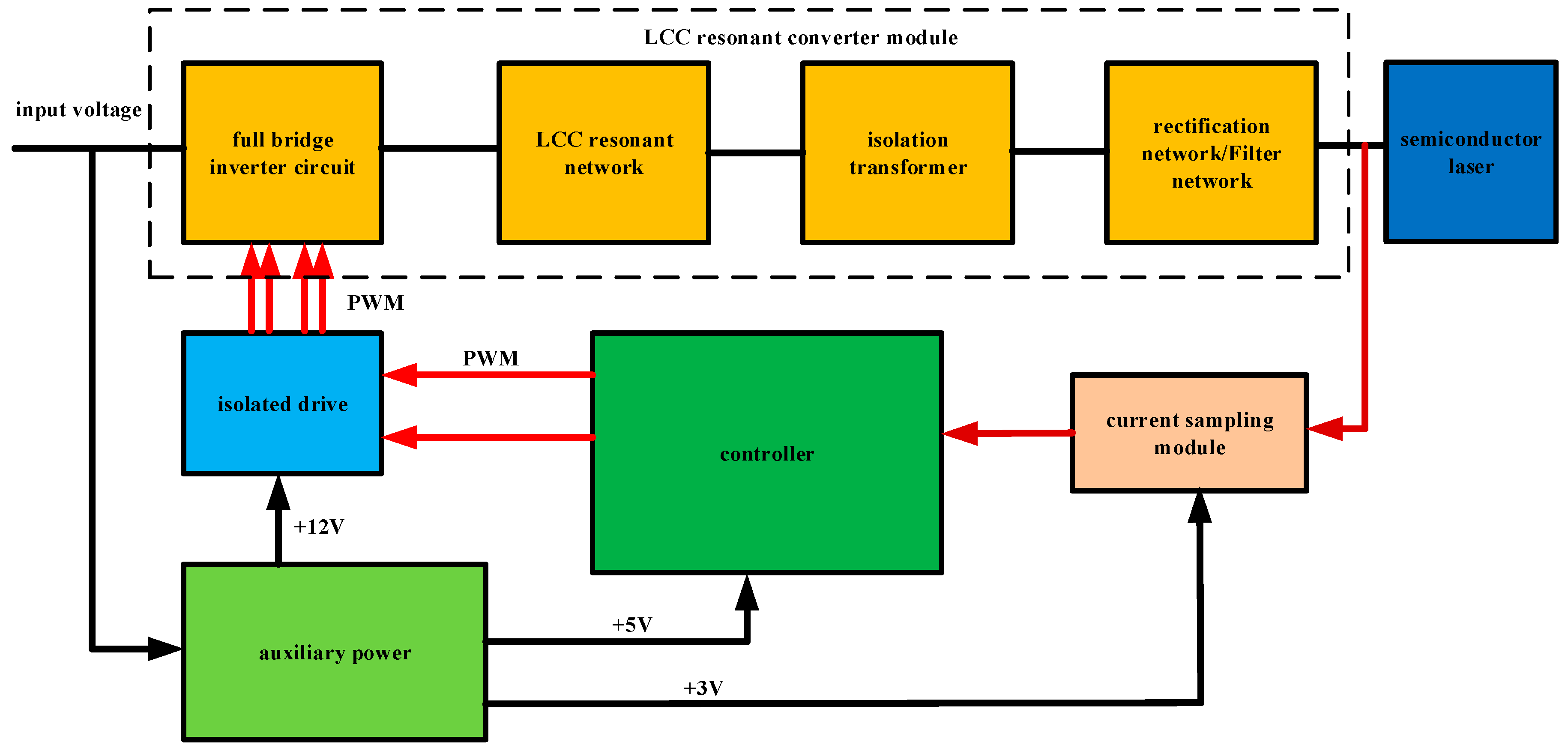
The proposed structure of the semiconductor laser power supply system is illustrated in Figure 1, comprising primarily of an LCC resonant converter module, a controller module, a current acquisition module, and an auxiliary power supply module.
The LCC resonant converter module, depicted in Figure 1, serves as the cornerstone of the power supply system by delivering a constant current. It encompasses a full-bridge inverter network, an LCC resonant network, a full-bridge rectifier network, and an LC filter network. The current acquisition module primarily samples the output current into the controller module, establishing a closed-loop feedback control mechanism. The controller module utilizes the appropriate algorithm to calculate the sampling current, thereby generating the signal that drives the MOS tube. It also assists in supplying power to the controller, drive circuit, and current sampling circuit.
Figure 1.
The power supply structure of semiconductor laser.
Figure 1.
The power supply structure of semiconductor laser.
2.1. Mathematical Model Analysis of LCC Resonant Converter
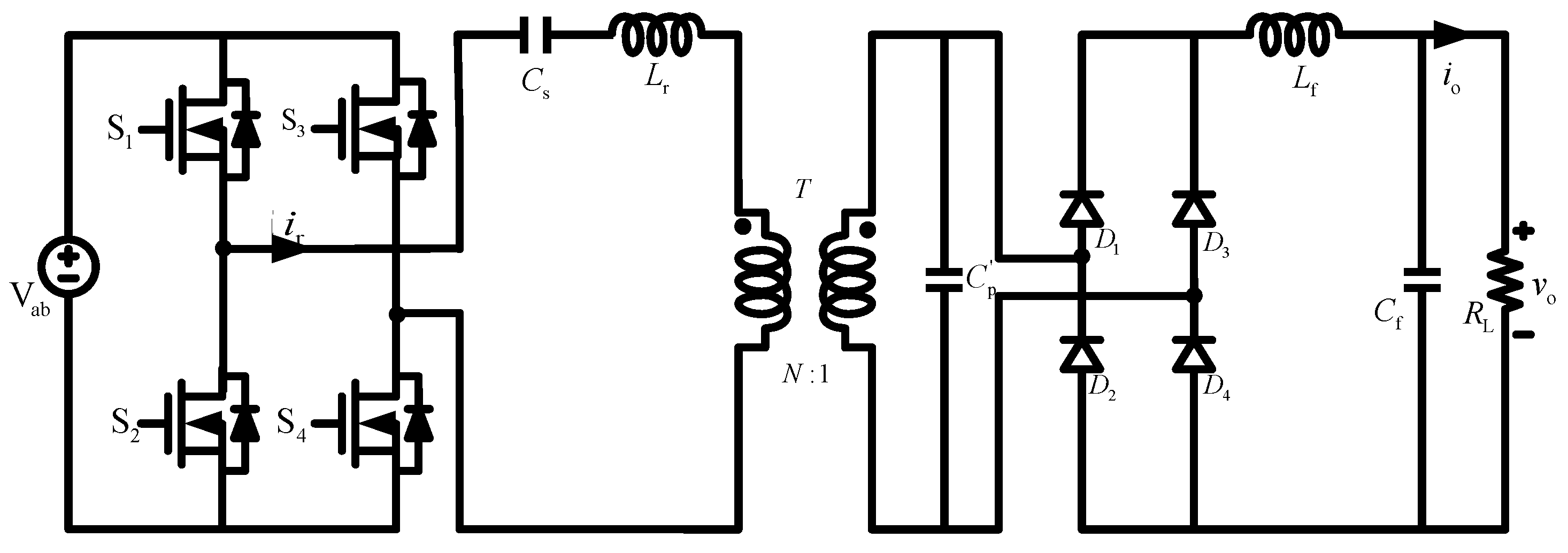
The topology of the LCC resonant converter is illustrated in Figure 2. From a topological perspective, the LCC resonant converter exhibits not only the characteristics of a series resonant converter for DC component isolation and transformer protection but also possesses wide-range input/output regulation capabilities akin to those of a parallel resonant converter. Consequently, it demonstrates excellent constant current source characteristics and robust output short-circuit resistance [19,20]. In order to optimize the volume of resonant converter, reduce the circuit current and circuit equivalent capacitance, increase the characteristic impedance of resonant network, and reduce the current stress borne by the converter, the parallel resonant capacitor() is designed on the secondary side of the transformer, so that the parallel resonant capacitor() and series resonant inductor() become parasitic parameters that cannot be ignored by the transformer under high frequency operation. It has good internal short-circuit protection function.
Figure 2.
The Topology of LCC resonant converter.
Figure 2.
The Topology of LCC resonant converter.
Because the mathematical model of LCC resonant converter is nonlinear, it is not conducive to the analysis of its working state, so it is necessary to linearize its nonlinear terms. When the frequency of the small-amplitude disturbed signal is much lower than the switching frequency of the system, the whole resonant converter can be considered as a quasi-steady-state system. In order to simplify the analysis, extended description function analysis [21,22] and linear differential equation theory are used to approximate the nonlinear terms, and the mathematical model of the steady-state system is obtained:
The output voltage
is:
io is the output current; vo the output voltage; irs and irc are amplitude of sinusoidal component and cosine component of resonant current ir respectively; are the amplitude of the sinusoidal and cosine components of the series resonant capacitor voltage , respectively; are the amplitude of the sinusoidal and cosine components of the series resonant capacitor voltage , respectively; ωs is the operating angular frequency; n indicates the ratio of turns of the transformer; vg indicates the input voltage; d represents duty cycle; iLf represents the current through the filtered inductor Lf; vCf represents the voltage of filter capacitor Cf. rc represents the ESR of the filter capacitance; RL indicates the resistance of the load.
Solve equations (1) through (9), The voltage gain of the open loop DC point of the LCC resonant converter is obtained:
represents the equivalent capacitance of the resonant network.
According to the relationship between voltage gain and current gain, the current gain can be obtained by normalizing equation (10):
ω=ωs/ωr, ωr is the angular frequency of the resonant network, , , , Zr indicates the characteristic impedance.
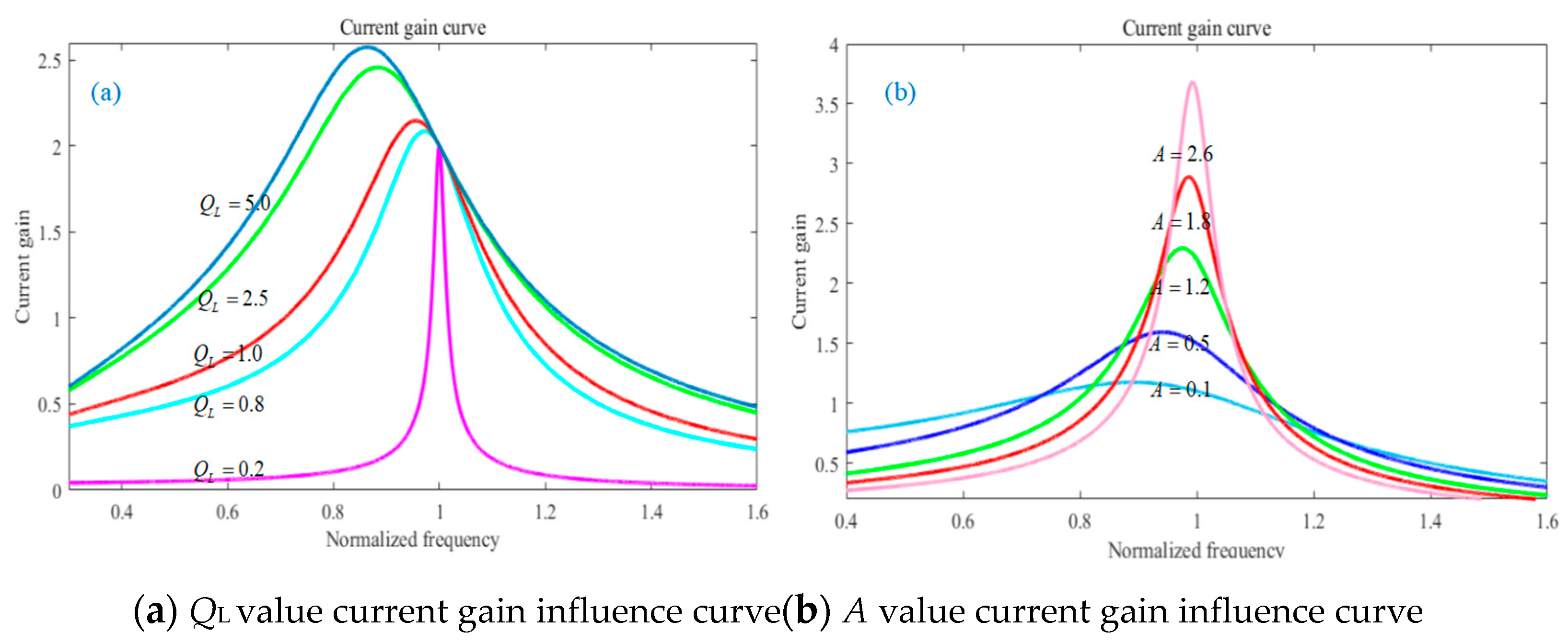
It can be seen from equation (11) that when ω=1, the LCC resonant converter exhibits constant current characteristics, and the output current is independent of the load, but only related to the input voltage and resonance parameters. When the LCC resonant converter works in this mode, the output current can remain unchanged even if the semiconductor laser load changes. In order to study the influence of current gain GI on QL, A, d and n, assuming A=n=1 and d=π, the change curve of current gain with different values of QL and A is drawn, as shown in Figure 3.
Figure 3.
Parameter influence curve of current gain.
Figure 3.
Parameter influence curve of current gain.
As can be seen from Figure 3(a), when the QF value increases continuously, the value of the current gain also increases. When the load is open (limQL→∞), the voltage gain GI will change sharply and tend to infinity, which will damage the power system in serious cases. When ω=1, the current gain is independent of the load, showing constant current characteristics; As can be seen from Figure 3(b), when the capacitance ratio (A value) increases, the current gain will change in the same direction as the A value, that is, with the increase of the A value, and when ω > 1, the smaller the A, the more gentle the current gain change.
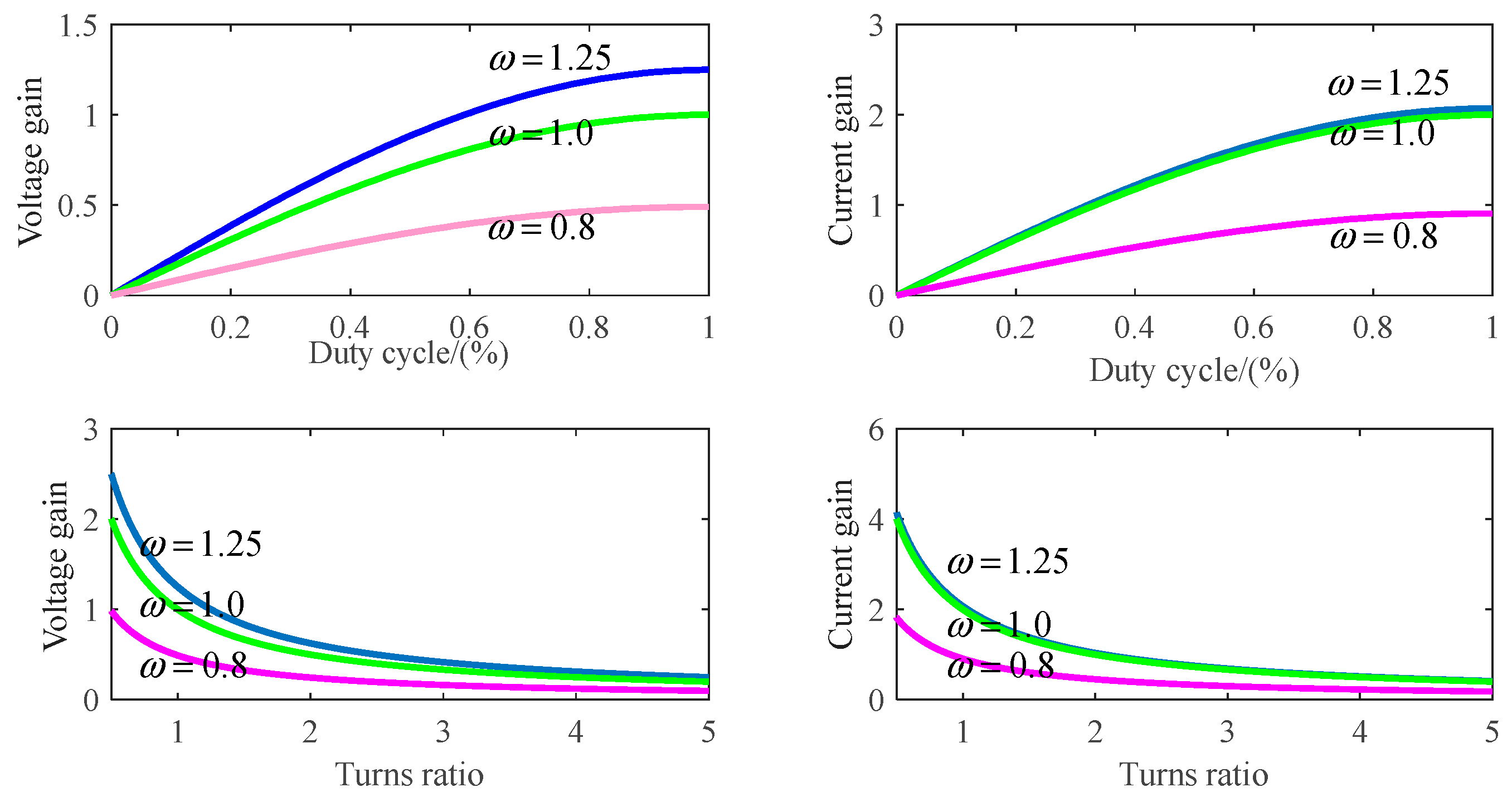
The values of duty cycle (d) and coil turns (n) of the transformer also affect the LCC resonant converter, and the gain influence curve of its output current and voltage is shown in Figure 4.
Figure 4.
Effect curve of d and n values on current-voltage gain.
Figure 4.
Effect curve of d and n values on current-voltage gain.
According to the influence curve of d value and n value on current-voltage gain, it can be seen that voltage gain and current gain change dramatically near ω=1. With the increase of d value, voltage gain and current gain increase, and decrease with the increase of n value, and when ω > 1, the smaller n or the larger d value, the more gradual the change of voltage and current gain.
2.2. Design of LCC Resonator Parameters
Ignoring the loss in the power transmission of the LCC resonant converter, the resonant current peak
Ir is obtained from the power conservation, which is expressed as:
Where, φ represents the impedance Angle.
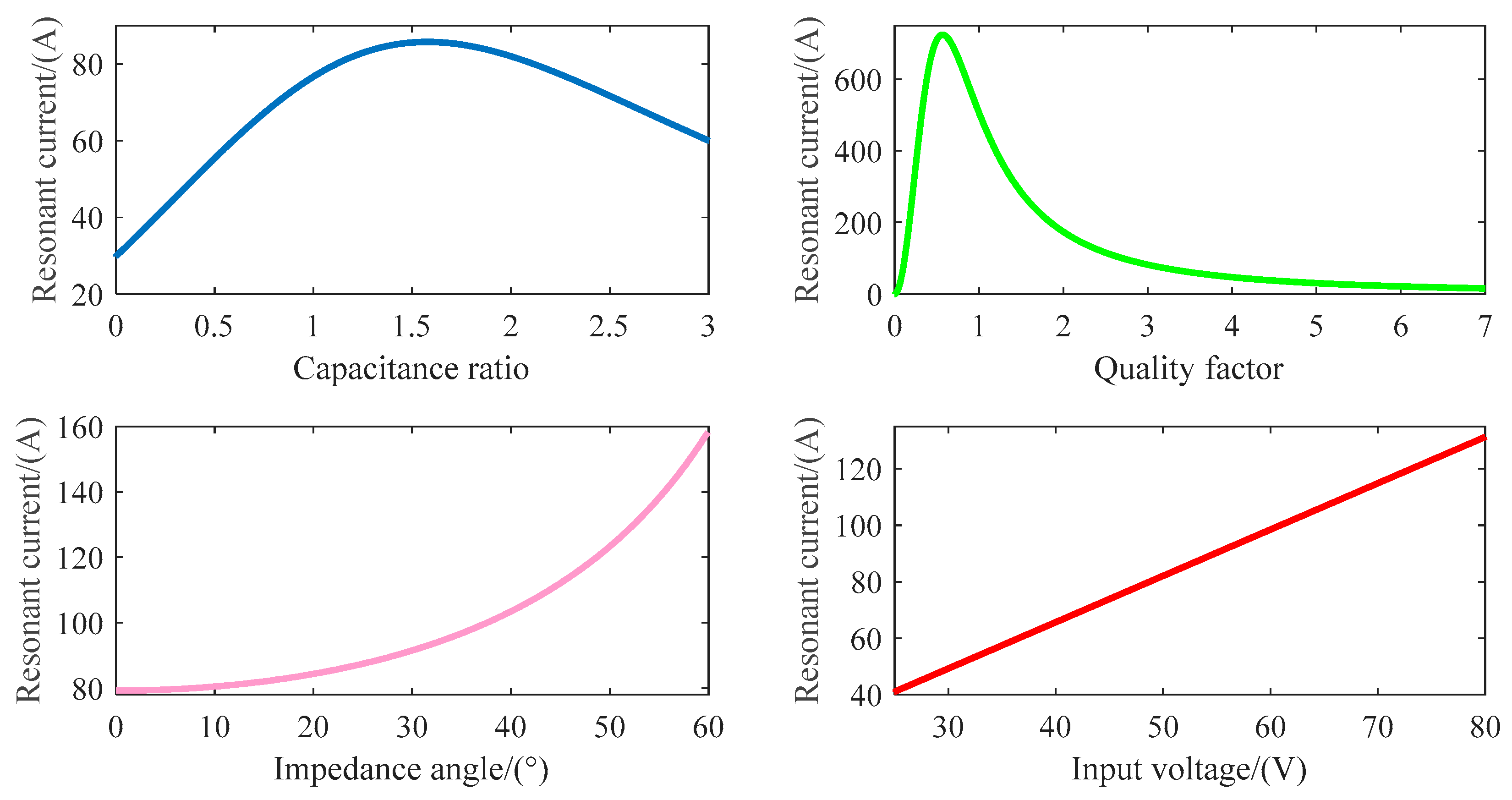
The characteristic curve of resonant current peak Ir affected by capacitance ratio A, quality factor QL, impedance Angle φ and input voltage Vi is shown in Figure 5. It can be seen from the characteristic curve that when the converter current gain, load and input voltage are constant, the smaller the φ is, the smaller the value of Ir is, and the smaller the current stress of the switching tube is. Only by ensuring φ > 0 can the ZVS conduction of the MOS tube be ensured, and sufficient margin is often left in the actual selection, generally within the range of 15° < φ < 30°. At the same time, too small quality factor and capacitance ratio will cause the resonant current peak to be too large, and the increase of input voltage will also cause the resonant current to increase.
Figure 5.
Resonant current peak characteristics.
Figure 5.
Resonant current peak characteristics.
In order to obtain more accurate parameters of the resonant network, reduce the current stress of the resonant components, and ensure that the resonant converter can achieve ZVS conduction, the following parameter design steps are given:
(1) The peak range of resonant current is determined according to input voltage, output power and output current;
(2) Select the appropriate resonant frequency and operating frequency range;
(3) The quality factor and capacitance ratio are determined according to the resonant current peak range;
(4) The transformer ratio n is calculated according to formula (13).
In formula (13), θ represents the conduction Angle of the rectifier tube.
(5) Finally, the LCC resonator parameters are calculated by formulas (14)-(16).
Series resonant capacitance:
Parallel resonant capacitance:
3. Power System Control Strategy and Algorithm Analysis
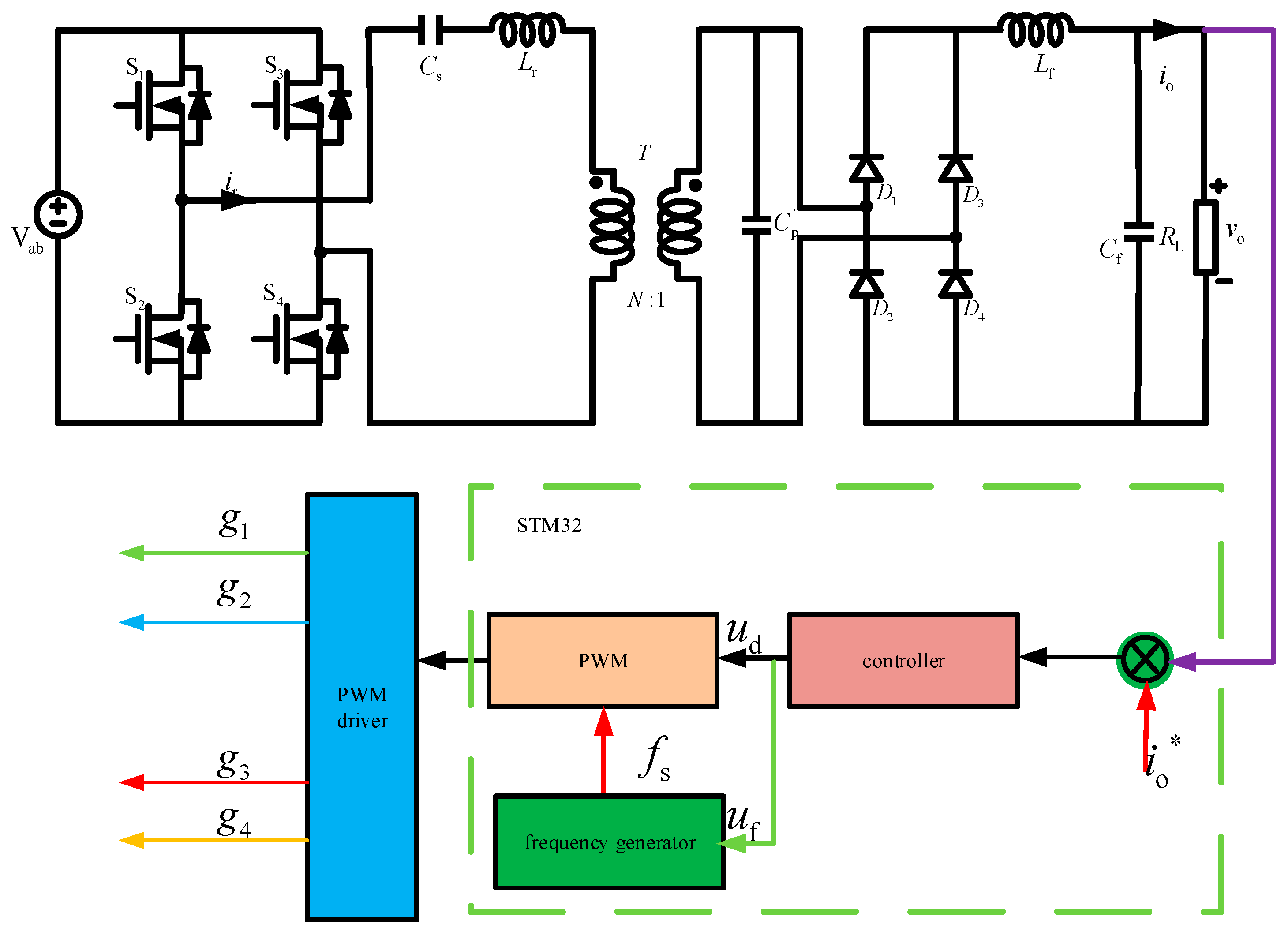
In order to overcome the disadvantages of the traditional control strategy, the variable frequency phase-shift composite control strategy is adopted, and its structure is shown in Figure 6.
In Figure 6, io* represents the given value of output current, ud and uf represent the control quantity of the phase and frequency of the controller output respectively, fs represents the carrier signal frequency, and g1~g4 represents the MOSFET drive signal respectively. This control strategy enables the controller to keep the output current stable by adjusting the switching frequency and the on-angle at the same time when the input/output changes, and still realize the soft switching under the condition of narrow switching frequency and wide input voltage/wide output range, thus improving the working efficiency and the service life of the device.
Figure 6.
Variable frequency phase shifting compound control strategy structure.
Figure 6.
Variable frequency phase shifting compound control strategy structure.
When the output current is increased, the increase of switching frequency fs will lead to the decrease of the on-angle φ. Therefore, under the combined action of fs and φ, the converter can achieve a wide input voltage in a narrow switching frequency range and achieve steady current output and soft switching under a wide output power condition.
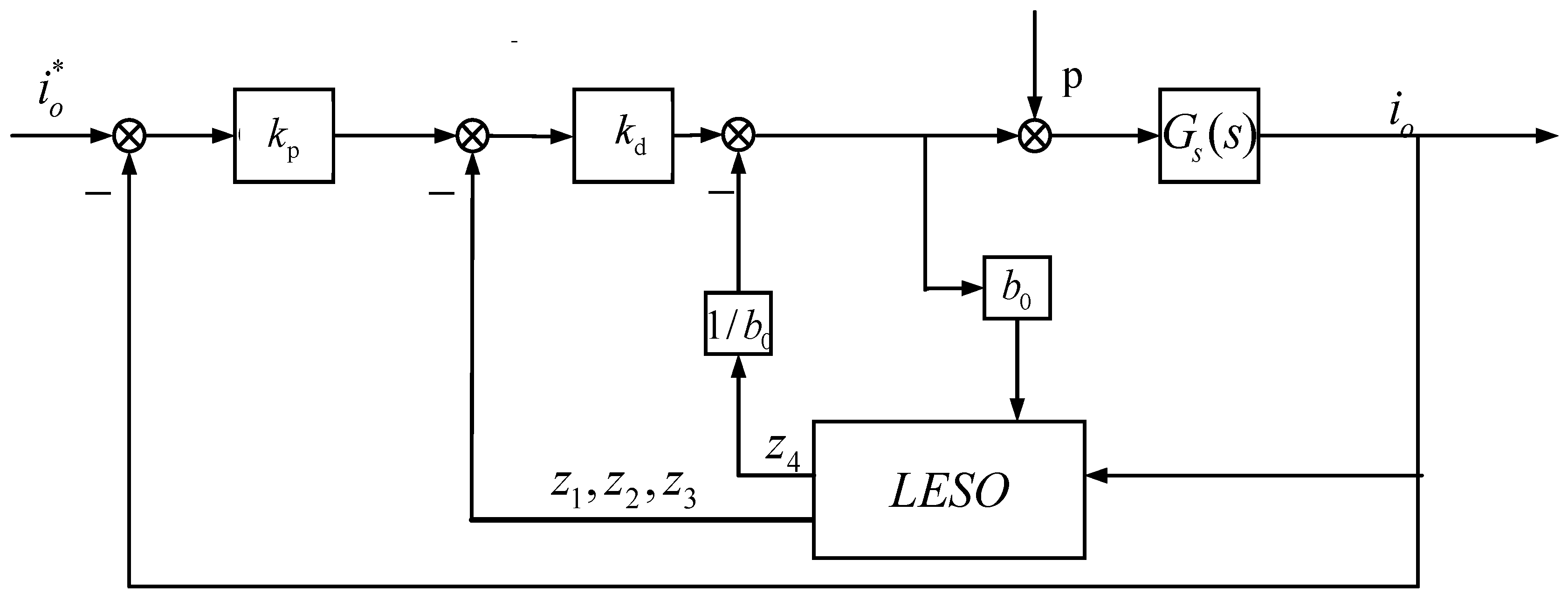
The traditional PID controller relies too much on the system model when designing parameters. In view of the complexity of the semiconductor laser load characteristics, the PID controller is easy to produce integral saturation and insufficient anti-interference ability, which makes the PID controller difficult to meet the design requirements. Therefore, the LADRC control algorithm is adopted, and its current loop structure is shown in Figure 7, where Gs(s) represents the control object transfer function, LESO represents the linear expansion observer, kp represents the scale coefficient of the controller, kd represents the differential coefficient, and b0 represents the compensation factor. The design of this algorithm does not depend on the exact model, and can observe and track the disturbance of the system in real time. It can overcome the shortcomings of PID controller and restrain the current instability caused by multi-factor disturbance.
Figure 7.
Linear active disturbance rejection current loop control algorithm.
Figure 7.
Linear active disturbance rejection current loop control algorithm.
The total disturbance p of the system can be estimated by the linear extended observer (LESO):
Where, u and y represent the input and output of the system respectively; L is LESO gain matrix; z is LESO state variable; is the output value estimated by the system.
The transfer function of LCC resonant converter can be approximated as a second-order system, so it is necessary to design a third-order extended observer to observe the system state and the total disturbance.
According to the bandwidth method [25], observer bandwidth
ωo, all poles of the extended observer are assigned in the left half plane, and the parameter tuning problem is simplified to the selection of observer bandwidth, and the corresponding observer gain is as follows:
The reconstructed system after disturbance compensation can be approximated as an integral series system. When the disturbance is observable, the second-order system can be reconstructed as a second-order integral series system by disturbance compensation. After disturbance compensation, the series integral system can obtain good control performance through simple linear error feedback rate control. The controller design is as follows:
Where, r represents the given input; represents the first derivative of a given input; u0 indicates the controller output.
4. Simulation and Test Results
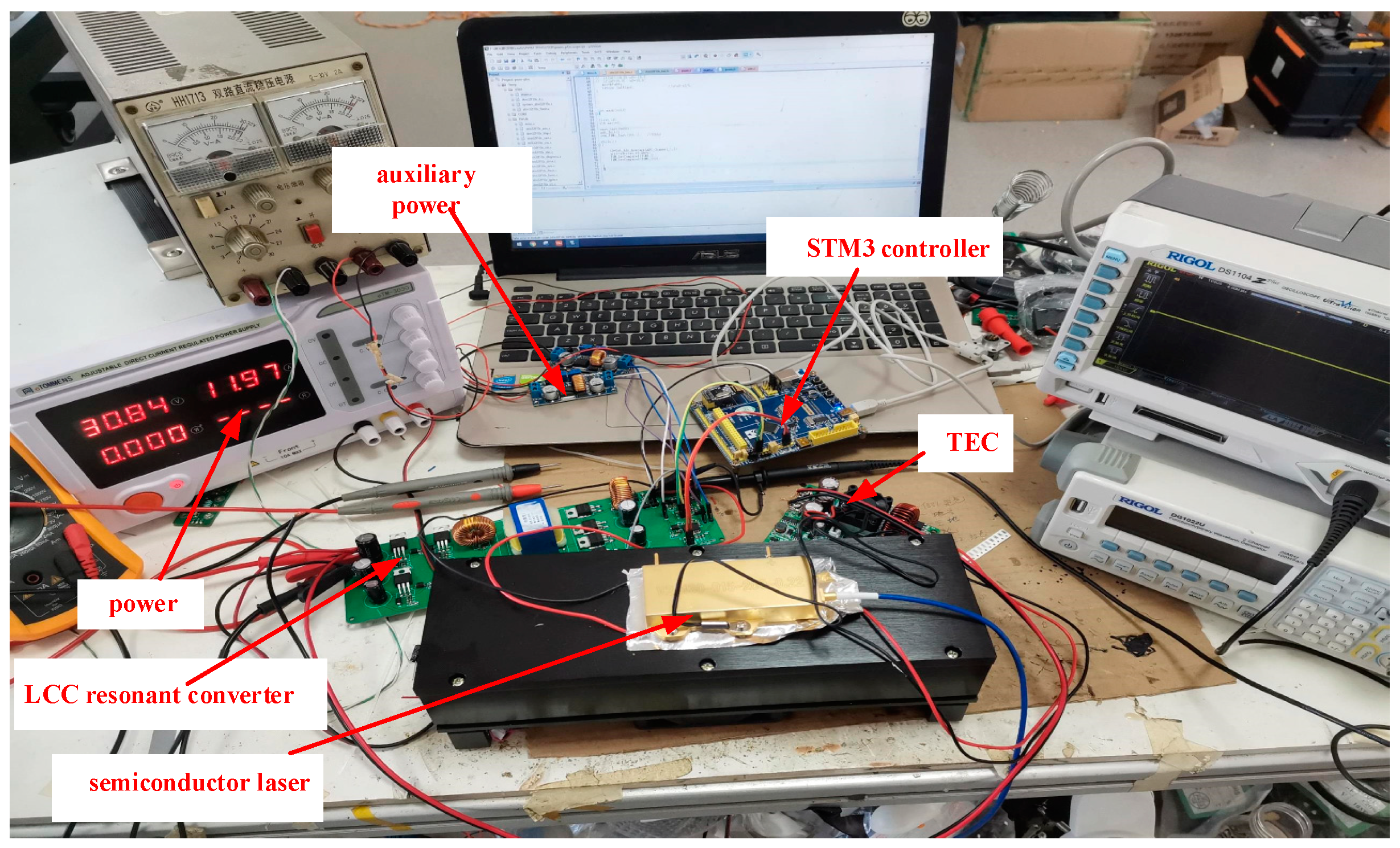
In order to verify the correctness of the semiconductor laser power supply scheme, Matlab/Simulink is used to build a semiconductor laser drive power supply simulation model. The prototype test platform with LCC resonant converter and STM32 controller as the core is shown in Figure 8. By testing the constant current output characteristic, anti-interference characteristic, working efficiency and ripple characteristic of the semiconductor laser driving power supply, it is proved that the design is reasonable and meets the design requirements.
Figure 8.
Prototype test platform.
Figure 8.
Prototype test platform.
The output voltage of the test prototype is 10~15 V, the output current is 0~40 A adjustable, the operating frequency is 51.5kHz, the resonant capacitor Cs is 354 nF, the resonant capacitor C’p is 9.03 μF, the resonant inductor Lr is 42.9 μH, and the transformer turns ratio n is 3.5.
4.1. Constant Current Characteristic Test of Semiconductor Laser Power Supply
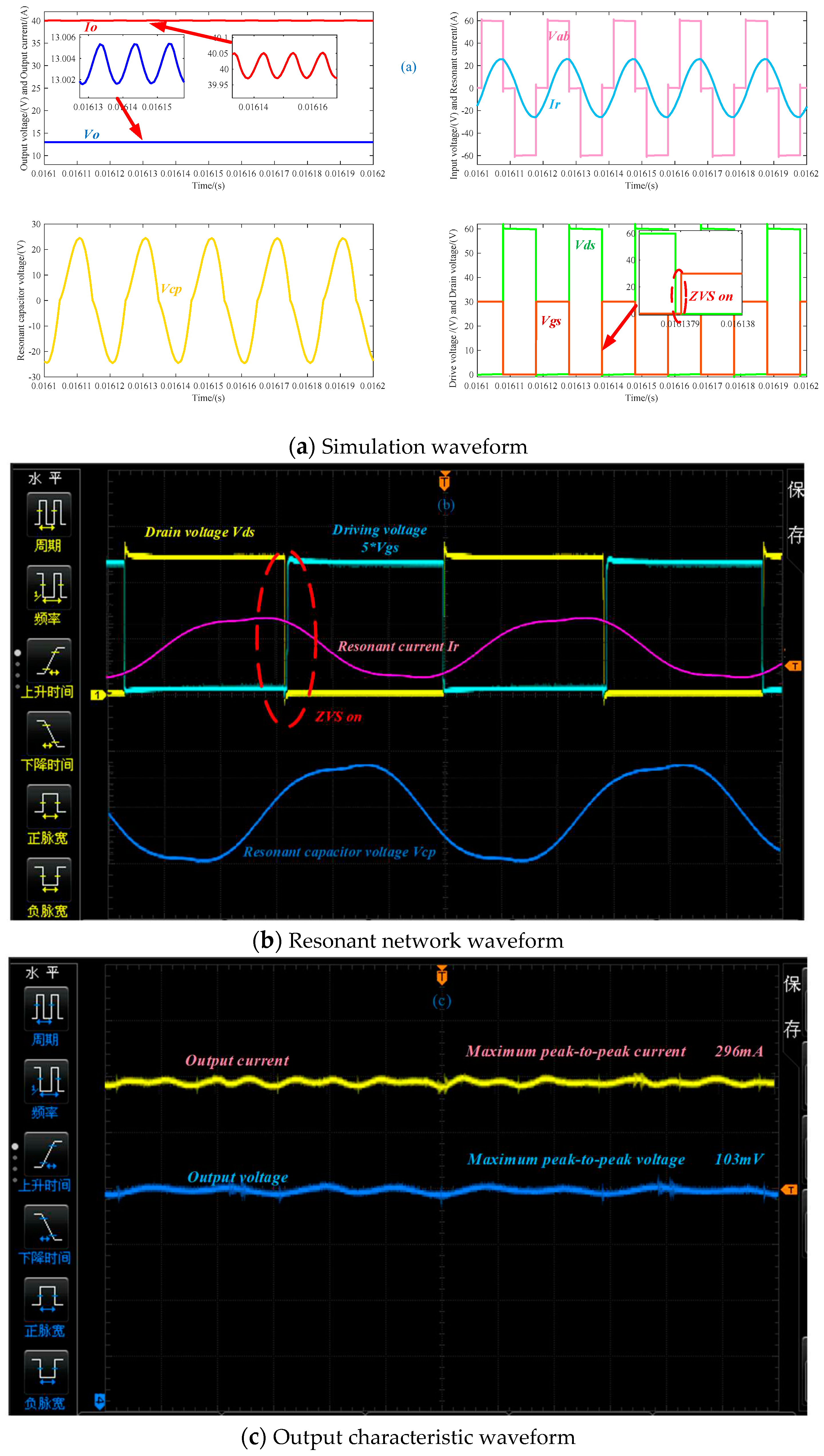
The simulation and test results of the constant current (40A) characteristics of the semiconductor laser power supply are shown in Figure 9, where Vgs and Vds are respectively the drive voltage and the drain-source voltage of the MOS tube, Vab is the input voltage of the resonant network, Ir is the resonant current, and Vcp is the shunt capacitor voltage. It can be seen from the simulation and test results that the variable frequency phase-shift composite control method extends the input voltage/output power range of the LCC resonant converter by synchronously adjusting the switching frequency and duty ratio, narifies the switching frequency range, and effectively reduces the current and voltage stress of the switching tube. The output current ripple coefficient is < 0.8%, and the output voltage ripple coefficient is < 0.45%. It can realize ZVS conduction under any power input voltage, effectively reduce the loss of power tube, and improve the performance of LCC resonant converter.
Figure 9.
Simulation and experimental results of constant current characteristics of semiconductor laser power supply.
Figure 9.
Simulation and experimental results of constant current characteristics of semiconductor laser power supply.
4.2. Experiment on Anti-Interference Characteristics of Semiconductor Laser Power Supply
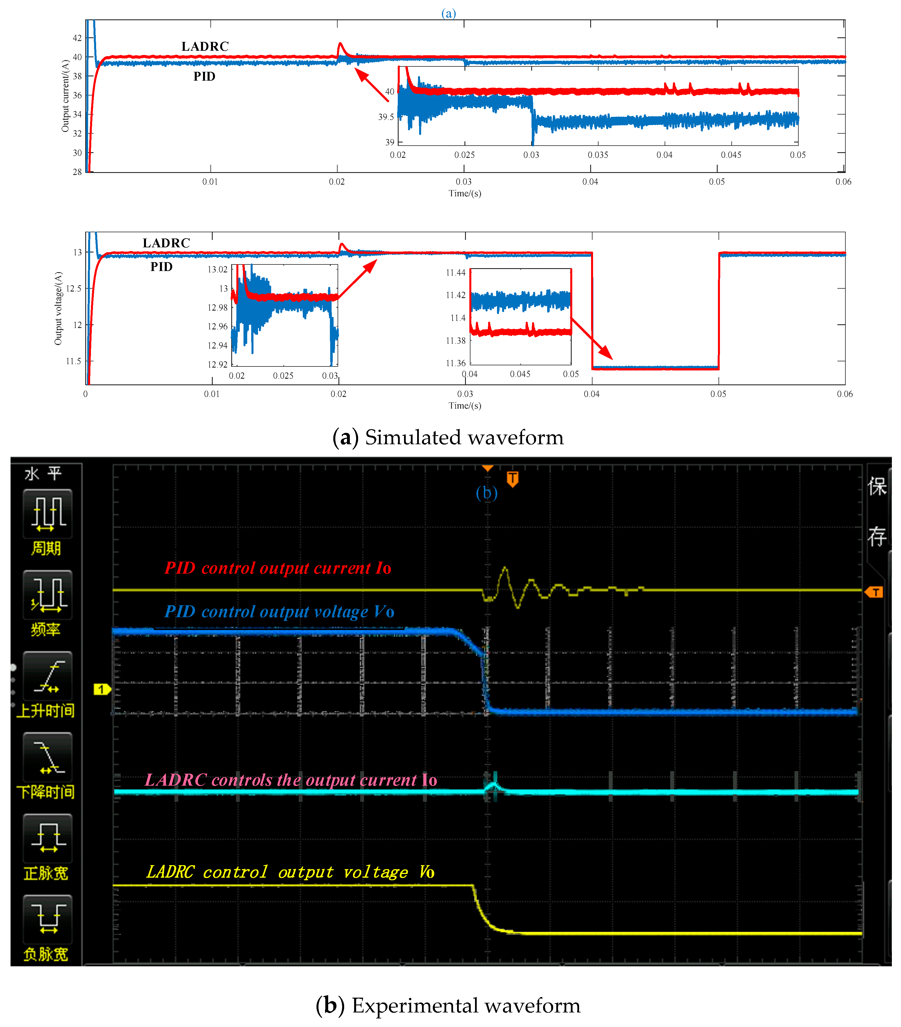
The simulation and test results of anti-interference characteristics of semiconductor laser power supply are shown in Figure 10. When t=0.02~0.03s, the input voltage Vin=60V changes to Vin=80V, and when t=0.04~ 0.05s, the load switches from full load to light load. According to the simulation and test results, the output current of the PID algorithm has a fast response speed, a large overjump, a large error and a large current ripple. When the input voltage or load is transformed, the ripple of the current and voltage increase and the current and voltage remain at the set value. Therefore, the LADRC algorithm has a good performance in anti-interference.
Figure 10.
Simulation and experimental results of anti-jamming characteristics of semiconductor laser power supply.
Figure 10.
Simulation and experimental results of anti-jamming characteristics of semiconductor laser power supply.
4.3. Power Efficiency Characteristic Test of Semiconductor Laser
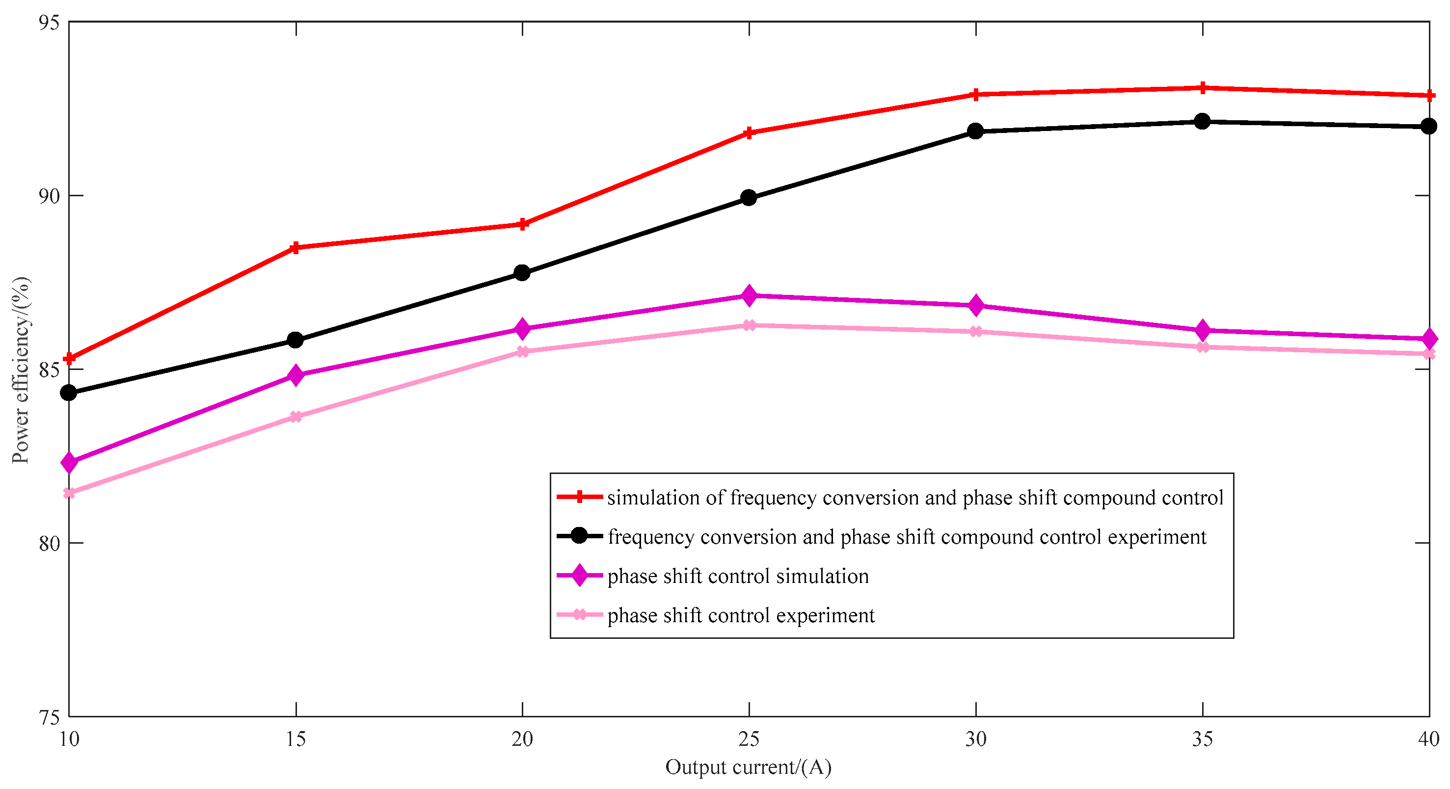
The simulation and test outcomes of the semiconductor laser power supply efficiency, as illustrated in Figure 11, reveal that the conventional frequency conversion control exhibits limited output adjustment capability and stability, leading to an overall low power supply efficiency. Consequently, only traditional phase shift control and composite control with frequency conversion phase shift are subjected to testing and analysis. Based on the simulation and test results, various control strategies yield differing power efficiencies; specifically, the phase-shifting control strategy induces hard switching states in the converter switch, thereby increasing switching losses and reactive power losses of the resonant converter. By implementing inverter phase-shifting compound control under full load conditions, a maximum power supply efficiency of 92% can be achieved concurrently with superior constant current characteristics.
Figure 11.
Simulation and experimental results of power efficiency of semiconductor laser.
Figure 11.
Simulation and experimental results of power efficiency of semiconductor laser.
5. Conclusions
The present study investigates the power supply system of high-performance semiconductor lasers, establishes a mathematical model of the LCC resonant converter, designs the parameters of the LCC resonant device, analyzes the drawbacks of conventional control strategy algorithms, and proposes the implementation of a frequency conversion phase shift compound control strategy and LADRC algorithm. This approach not only enhances the power supply efficiency of semiconductor lasers but also reduces the current stress on the device. Furthermore, it achieves zero-voltage-switching (ZVS) of the switching tube, minimizes switching losses, and exhibits strong anti-interference capabilities. These unique characteristics of the LCC resonant converter make it suitable for high-performance semiconductor laser drive power supplies.
Acknowledgments
This research was funded by Shaanxi Science and Technology Department (Program No.2020GY-158) and 2022 “Insight Action” Achievement Transformation and Application Project (Program No.628020320). The authors thank all the anonymous reviewers for their very helpful comments to improve the paper.
References
- Yang, Y.F. Research on high power semiconductor laser. Electron. Compon. Inf. Technol. 2022, 6, 41–43. [Google Scholar]
- Ning, Y.Q.; Chen, Y.Y.; Zhang, J.; et al. Brief review of development and techniques for high power semiconductor lasers. Acta Opt. Sin. 2021, 41, 191–200. [Google Scholar]
- Liu, X.X.; Han, J.H.; Cai, H.; et al. Review of high repetition-rate mid-infrared lasers for photoelectric countermeasures. Laser Technol. 2021, 45, 271–279. [Google Scholar]
- Xu, Y.F.; Shi, Y.J.; Shao, J.Z.; et al. Design of high precision pulse power supply for high power semiconductor laser. Laser Technol. 2023, 47, 108–114. [Google Scholar]
- Tian, Y.L.; Li, C.S.; Zhang, Z.Y. High-accuracy and high-stability constant current power for semiconductor lasers. J. Xi’an Jiaotong Univ. 2019, 53, 1–5. [Google Scholar]
- Yang, C.L.; Jia, H.Z.; Xia, G.Z. Design for the circuit to eliminate surge of the laser diode power supply. Appl. Laser 2008, 28, 310–313. [Google Scholar]
- Wu, J.W.; Qi, Y.; Wu, X.K. High-efficiency laser diode driver for aerospace applications. Aerosp. Shanghai (Chin. Engl.) 2020, 37, 81–87. [Google Scholar]
- Thompson, M.T.; Schlecht, M.F. High power laser diode driver based on power converter technology. IEEE Trans. Power Electron. 1997, 12, 46–52. [Google Scholar] [CrossRef]
- Yang, J.T.; Wang, J.A.; Wang, Y.; et al. Design and research of a new high performance power supply for semiconductor lasers. Chin. J. Electron Devices 2021, 44, 817–823. [Google Scholar]
- Zhao, Q.L.; Li, S.; Cao, R.R.; et al. Design of pulse power supply for high-power semiconductor laser diode arrays. IEEE Access 2019, 7, 92805–92812. [Google Scholar] [CrossRef]
- Zhang, L.; Chen, J.S.; Gao, J.; et al. Design of driving power and temperature control system for high power semiconductor laser. Infrared Laser Eng. 2018, 47, 102–108. [Google Scholar]
- Liu, J.N.; Zheng, H.; Sun, Y.H.; et al. Research on a multi-branch micro-second laser drive power and control technology for laser cleaning. Chin. J. Electron Devices 2021, 44, 322–327. [Google Scholar]
- Zhang, Z.F.; Zhai, Y.S.; Zhan, S.U.; et al. A novel method to drive semiconductor laser for optical frequency standard based on constant voltage source. Optik 2015, 126, 3924–3926. [Google Scholar] [CrossRef]
- Orietti, E.; Mattavelli, P.; Spiazzi, G.; et al. Analysis of multi-phase LLC resonant converters[C]//2009 Brazilian Power Electronics Conference. Bonito-Mato Grosso do Sul, Brazil. IEEE, 2009: 464-471.
- Hyeon, B.C.; Cho, B.H. Analysis and design of the $LmC$ resonant converter for low output current ripple. IEEE Trans. Ind. Electron. 2012, 59, 2772–2780. [Google Scholar] [CrossRef]
- Lü, Y.; Gao, J.Y.; Jiang, Y.J. Design of efficient power supply for high power infrared laser diode. Laser Infrared 2019, 49, 309–314. [Google Scholar]
- Wang, C.; Ma, X.M.; Yu, P.P.; et al. Research of laser diode driver with interleaved single ended forward conversion. Laser Technol. 2016, 40, 665–669. [Google Scholar]
- Zhong, X.L.; Wang, J.; Luo, Y.H.; et al. Research on power control system of semiconductor laser with active temperature. Appl. Laser 2021, 41, 608–613. [Google Scholar]
- Zhao, Q.L.; Cao, R.R.; Wang, D.Y.; et al. Design of pulse power supply for diode pumped solid state laser. High Power Laser Part. Beams 2018, 30, 129–134. [Google Scholar]
- Cao, R.R.; Wang, D.Y.; Zhao, Q.L.; et al. Wide range voltage of diode laser driver. High Power Laser Part. Beams 2018, 30, 12–15. [Google Scholar]
- Yuan, Y.S.; Yi, C.Y.; Peng, N. T-type half-bridge LCC resonant converter with L-R composite modulation. Trans. China Electrotech. Soc. 2022, 37, 892–904. [Google Scholar]
- Liao, H.F.; Shuai, D.X.; Long, T.Y. Research on Li-ion battery charger based on LCC resonant converter. Chin. J. Power Sources 2021, 45, 669–672. [Google Scholar]
- Zhan, L.N.; Wang, C.F.; Ma, C. Modeling of LLC resonant converter based on extended describing function method. Syst. Simul. Technol. 2014, 10, 211–216. [Google Scholar]
- Hu, F.Z.; Xiong, J.F.; Qi, C.C. Modeling and analysis of bidirectional full-bridge CLLLC resonant converter. J. Air Space Early Warn. Res. 2019, 33, 446–450. [Google Scholar]
- Ma, M.; Liao, P.; Cai, Y.X.; et al. First-order active disturbance rejection control and parameter tuning method based on particle swarm optimization for LCL grid-connected inverter. Electr. Power Autom. Equip. 2021, 41, 174–182. [Google Scholar]
|
Disclaimer/Publisher’s Note: The statements, opinions and data contained in all publications are solely those of the individual author(s) and contributor(s) and not of MDPI and/or the editor(s). MDPI and/or the editor(s) disclaim responsibility for any injury to people or property resulting from any ideas, methods, instructions or products referred to in the content. |
© 2023 by the authors. Licensee MDPI, Basel, Switzerland. This article is an open access article distributed under the terms and conditions of the Creative Commons Attribution (CC BY) license (http://creativecommons.org/licenses/by/4.0/).
