1. Introduction
In recent years, there has been an increasing demand for faster internet with an exponential growth in the number of online-connected applications and their number of users [
1]. To meet the projected demand, wireless data rates in the terabit per second range are required. These rates are achievable with higher bandwidths offered in the terahertz (THz) band (0.1 to 10
) of the electromagnetic (EM) spectrum [
2]. Currently, many applications are expected to benefit from short-range wireless connectivity in the THz domain. For example, wireless networks on chip (WNoC) [
3] presents the opportunity for on-chip and chip-to-chip communication, combating wiring delays and increasing the compactness of input/output (I/O) ports. Similarly, wireless nanosensor networks [
4], comprised of chemical sensors, biosensors, and physical sensors, and their integration with macroscale networks in the so-called Internet of Nano-Things [
5] will enable transformative applications in the industrial, biomedical, and military fields. However, the progress in these areas is hampered by the lack of a compact, efficient, room-temperature operating THz source for high-power, low-noise radiation.
One of the most promising approaches to developing an active THz source is to use electron plasma oscillations in the two-dimensional (2D) electron channel of field-effect transistors (FETs). Recent experiments in graphene FETs demonstrated high-quality 2D electron plasma oscillations in the THz domain at room temperatures [
6,
7]. The compact FET size (roughly a few microns), its compatibility with planar CMOS technology, and the ease of external control of the plasma amplitude and frequency make FETs a very attractive candidate for the development of a tunable THz source. Our previous works involve the development of the muliphysics simulation platform of a graphene-based plasmonic THz generator [
8], designing the FET based on experimental setups [
9], and integrating on-chip modulation to the FET [
10].
While plasmonic FETs offer a compact package for THz signal generation, the EM radiation often lacks gain and directivity. To combat this issue, several passive elements can be applied to the devices to help bridge the THz gap, such as graphennas [
11,
12,
13]. Graphene supports the propagation of tightly confined Surface Plasmon Polariton (SPP) waves with a reduction of propagation speed in comparison to its vacuum EM propagation speed counterpart. These graphene-based plasmonic nano-antennas take advantage of the high confinement factor in graphene, reducing the antenna size to a few
m, up to two orders of magnitude below the size of metallic antennas in the THz regime [
14]. The radiation pattern of a graphenna is similar to an equivalent metallic antenna, with comparable efficiencies. This compact setup and ease of integration fit well in WNoCs and other nanosystem applications. However, for longer propagation distances a larger radiating element is required, such as a metallic antenna.
In addition to graphennas, lenses may be applied to directional antenna and graphenna systems to further enhance their radiation efficiency, or applied directly to the source. Terahertz lenses can be implemented in several ways, such as fixed, typically with dielectric materials [
15,
16], or programmable, typically with metamaterials [
17,
18], coming in a hemispherical shape of a few hundred microns to a few hundred millimeters in size. Their simplicity allows seamless integration into several THz systems, such as waveguides, horn antennas, antenna array systems, on-chip antennas, and FETs, to name a few.
Traditional metallic antennas for passive THz emission, reviewed in [
19], include horn antennas [
20], dipole antennas, and microstrip antennas [
21], and provide a larger output power due to their large size. Horn antennas offer a highly directive, rotationally symmetric beam pattern with a gain above 30 dBi, low cross-polarization level of -30 dB with 98% coupling efficiency [
22,
23]. Microstrip antennas, a substrate-based planar antenna, come in a variety of forms such as butterfly, U-shaped, log-periodic, and patch antennas. While microstrip antennas typically exhibit a lower gain compared to horn antennas [
24], this trade-off is offset by their inherent advantages, including a compact form factor, ease and low cost of fabrication, and higher degree of tunability, enabling precise impedance matching and optimization of their radiative performance.
In this study, we design a graphene FET THz source integrated with a microstrip patch antenna, facilitated through a tailored metamaterial feed structure. A microstrip patch antenna is chosen for its ease of implementation and integration into the FET system without destroying the asymmetric boundary conditions required for our device setup. Leveraging our computational framework, which self-consistently solves electron transport and electromagnetic equations in MATLAB [
8] with antenna engineering simulations in COMSOL, we aim to optimize the radiation characteristics of the FET-antenna system. The graphene-based FET is constructed based on our previously developed model [
9]. It features the asymmetric geometry [
25] designed to facilitate the boundary conditions required for the implementation of the Dyakonov-Shur (DS) instability in the transistor. This instability induces the onset of plasmonic oscillations in the FET channel within the THz frequency band. To enable efficient coupling from the plasmonic channel to the gate and subsequently sufficient current flow to the antenna via the feed, we employ a Hyperbolic Metamaterial (HMM) in the gate/feed system. Our results show that the proposed antenna and feeding system enhance the radiation from the graphene FET by nearly 20 times.
2. Materials and Methods
The proposed device amalgamates a microstrip patch antenna with a FET featuring a graphene channel. This union is achieved through a meticulously engineered feed structure, with the key importance of not breaking the asymmetric boundary conditions of the DS instability. The device architecture encompasses several integral components, each designed to facilitate active, efficient THz signal radiation. This section breaks down the system into several components to present the intricacies of the device geometry.
2.1. Field-Effect Transistor
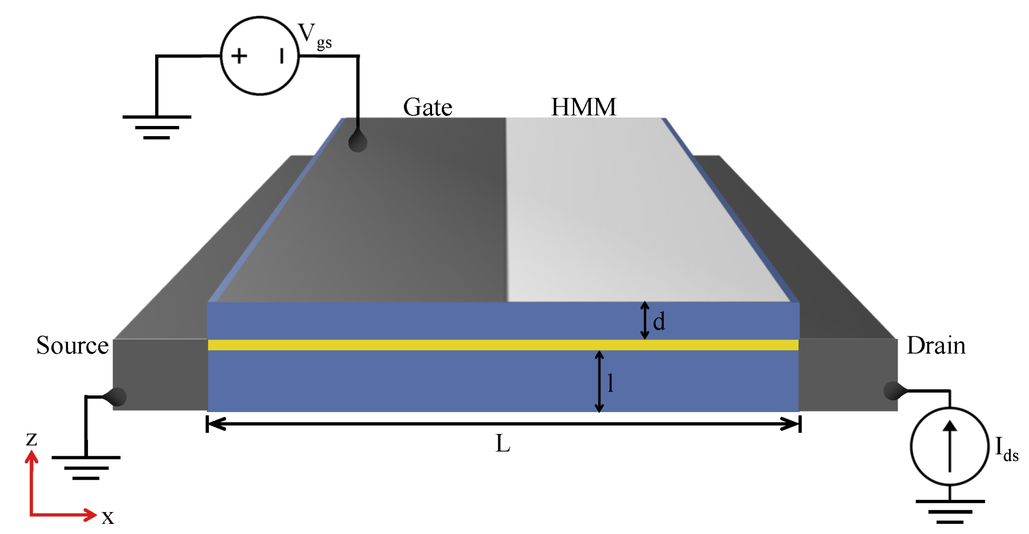
At the core of our device lies the FET, displayed in
Figure 1, a critical component in the system in charge of generating the THz signal. The graphene layer serves as the plasmonic cavity with a channel length (
L) of 1
m, sandwiched between two silicon dioxide (SiO
2) dielectric layers serving as the top barrier and bottom substrate, with depths of
d = 35 nm and
l = 4.95
m, respectively. A metallic reflector is placed below the substrate to confine the EM waves within the device. The gate contact is asymmetrically positioned atop the dielectric barrier closer to the source contact, giving rise to an asymmetrical configuration. Superimposed upon the upper SiO
2 layer to the right of the metallic gate is the HMM – a pivotal element in our device’s functionality.
The physical mechanism to convert the plasma oscillations in the FET electron channel into an EM signal was proposed by Dyakonov and Shur in Ref. [
26]. The authors theoretically demonstrated that in a FET biased by a DC current with a plasmonic cavity formed in the FET channel, the plasma wave amplitude may exponentially increase after multiple reflections from the source and the drain contacts. This instability occurs if asymmetric boundary conditions are imposed at opposite ends of the plasmonic cavity for plasma wave reflections. Specifically, a large AC impedance between the ohmic contact and the gate at one side of the FET cavity (the drain side,
) and a small AC impedance at the opposite end (the source side,
) when a DC current flows from the drain to the source. In the instability endpoint, stationary sustained plasma oscillations are developed in the plasmonic channel and the energy supplied by the DC current is balanced by Joule losses and radiation [
8,
27,
28].
In early works, ideal boundary conditions with the gate-source impedance
and the gate-drain impedance
were assumed [
26]. It was later shown that the DS instability takes place at any finite boundary impedance provided that
and Joule losses are sufficiently small [
9,
29]. Practical implementations of the finite asymmetric boundary impedances rely on geometric asymmetry in the FET. Previous experimental demonstrations were exploited by shorting the source and gate contacts [
30], asymmetrically positioning the gate contact with respect to the source and drain contacts [
31], depleting the channel on one side, and an engineered FET structural asymmetry [
25]. Consequently, resonant THz emission at plasma frequencies tunable by the gate voltage was observed. Transport measurements in these structures demonstrated sustainable plasma oscillations in the FET cavity consistent with the DS instability. Our simulated FET utilizes a combination of asymmetries to realize the DS instability in the plasmonic cavity for THz signal generation, including the applied gate voltage
asymmetrically depleting the channel, with the applied current
ensuring electron flow for the plasmonic cavity.
2.2. Microstrip Patch Antenna and Feed
The microstrip patch antenna, a vital component for efficient THz signal radiation, is meticulously designed to maximize its radiative efficiency. It features a width of 120 m and a length 64.1 m. An imperative feature of the patch antenna is the simplistic control of the impedance to match the FET-feed structure. Strategic perforations in the patch antenna near the feed and precise choice of permittivity values for the substrate and feed are adopted to optimize both radiation efficiency and impedance matching. The depth of the patch substrate, feed, and FET substrate are consistent at l = 4.95 m. This depth allows the EM waves generated from the instability and reflected from the bottom metallic layer to constructively interfere in the FET, and allows efficient radiation in the THz regime for the microstrip patch antenna.
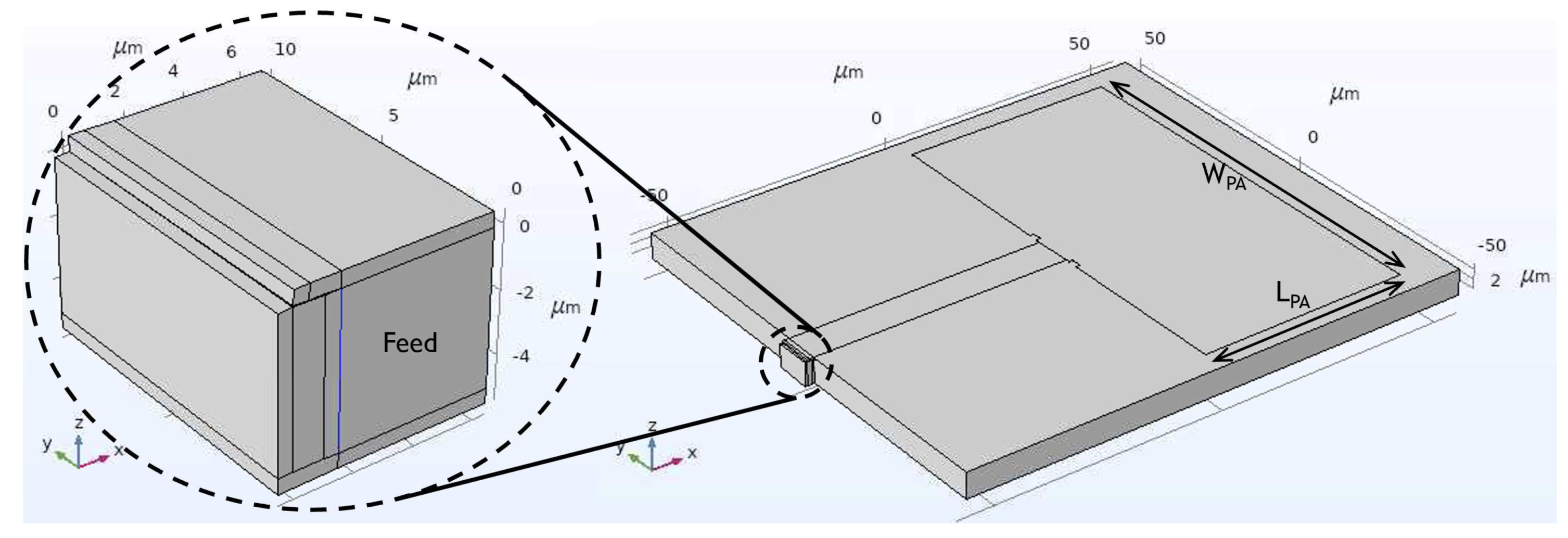
The feed structure, seamlessly integrated with the antenna, is strategically situated to the right of the FET’s drain contact, where the gate that carries the current continues to the feed top contact (shown in
Figure 2). It features dimensions of 60.5
m in length (
) and 8
m in width (
). The gate, contacts, and bottom reflector of the FET effectively contain the electromagnetic radiation within the enclosed region. This containment augments the coupling efficiency of plasmonic waves in graphene with the gate. Concurrently, the metallic bottom layer of the feed structure acts as the grounding plane for the feed and antenna, establishing a comprehensive electromagnetic circuitry.
Figure 3 provides an overview of the entire setup encompassing the FET, feed, and microstrip patch antenna, with a detailed zoom-in on the FET structure.
2.3. Hyperbolic Metamaterial
The employment of the HMM as a pivotal element in our device architecture is substantiated by its anisotropic behavior suitable to our objective. The dispersion of the HMM conforms to a hyperboloid shape [
32], with one directional component of permittivity (
) extending infinitely in the direction where
is negative. Effective metamaterials with hyperbolic dispersion have been experimentally realized using layered metal-dielectric structures in a repeated stack, or via nanowire arrays, in the THz regime [
33], generally achieved using a semiconductor such as graphene as opposed to a metal in the layered structure [
34], and more in the optical range [
35], for sub-wavelength imaging [
36,
37], focusing [
38], and other applications [
39,
40,
41].
Notably, the HMM plays a dual role, functioning as both a dielectric in the out-of-plane direction and a metal in the in-plane direction. Precisely, the properties of the HMM are harnessed to behave as a dielectric in the direction where the permittivity (
) is negative, while concurrently behaving as a metal in the orthogonal direction [
42]. This utilization of the HMM endows us with the sought-after asymmetry in gate-source and gate-drain capacitances and impedances. Note the asymmetry is only in the
z direction, but our numerical simulations have demonstrated this is sufficient for the onset of the DS instability.
Furthermore, the regions of the dispersion relation that extend to infinity signify the existence of extremely large wavevectors (
k) or infinitesimally short wavelengths (
) that satisfy the equation. This, in turn, implies the presence of an unbounded photonic density of states within the material, rendering it exceptionally efficient for both radiation and absorption processes. The plasmonic oscillations in the channel are efficiently coupled to the metallic gate and the HMM. In our device configuration, the HMM assumes the role of a metal type (Type II,
and
) on the right side of the gate, aligned parallel to the two-dimensional electron gas (2DEG), while acting as a dielectric in perpendicular dimension (
z). The effective dielectric tensor components for the parallel
and perpendicular
direction with respect to the anisotropy axis is given by [
43]
where
(
) is the thickness and
(
) is the dielectric constant of the metallic (dielectric) component. By tuning these parameters such that
, one can attain the hyperbolic regime. This type II configuration facilitates the controlled flow of current into the antenna.
3. Simulation Platform
In this section, we explain in detail the simulation platform utilized to comprehensively investigate the performance of the proposed microstrip patch antenna with an integrated graphene-based FET. The simulation methodology involves a dual-stage approach: first, we model the FET and feed system using MATLAB, where hydrodynamic equations for electron transport in graphene and Finite-Difference Time-Domain (FDTD) techniques for EM field modeling are employed, derived in [
8] and [
9]. The dimensions and complexity of the FET make MATLAB the suitable choice for the transient response of the system. Subsequently, we employ COMSOL Multiphysics to simulate the microstrip patch antenna. The larger dimensions of the patch antenna make COMSOL the suitable choice for the radiative characteristics of the system. Our previous attempts showed a transient response of the FET too long for the iterative solver to be modeled in COMSOL, and antenna dimensions too large for the FDTD solver in MATLAB. However, the FET is modeled in COMSOL without the DS instability transient response to ensure impedance matching and to minimize reflections. This dual-stage simulation strategy enables us to address the inherent complexities of the device.
3.1. MATLAB-Based Simulation of the FET and Feed System
The FET and feed system are primarily modeled in MATLAB, where we employ hydrodynamic equations for electron transport in graphene. These equations encompass critical parameters such as electron density (
n), electron current density (
j), and drift velocity (
v), which are interconnected through the relationship
. The electron density (
) is initialized with a depleted region following the Fermi function dependent on the applied gate voltage, and (
) is updated in the iterative loop using the continuity equation,
We utilize the Euler equation augmented with a scattering term to model the electron current density (
). The Euler equation for massless 2D Dirac fermions to describe the electron dynamics in the DC current-biased graphene layer has the form
Here
,
is the equilibrium electron density,
is the drift velocity due to stationary electron flow
in the channel,
is the electron momentum relaxation time,
is the electron Fermi velocity in graphene, and
is the electron charge. The self-consistent electric field
is induced by the charged fluctuations in the electron system. For electron channels with non-uniform equilibrium electron density
considered in this paper, the electric field
includes a static built-in electric field
producing the non-uniform equilibrium electron density distribution. The total field
is split in Eq. (
3) as
, where
is the induced electric field. A small “kick” is applied to the initial current density for the onset of plasmonic reflections in the channel. These equations form the basis of our iterative solver, facilitating the study of charge transport in graphene within the FET.
To couple the EM field interactions, we employ the FDTD method to solve Maxwell’s equations. Specifically, we solve for the current density (
) using the hydrodynamic solver and subsequently input this current density into the FDTD-based EM solver to compute the electric field component (
),
where
and
are the electric and magnetic components of the EM field induced by the electric current
in the channel. This electric field distribution (
) is then fed back into the hydrodynamic solver, creating a closed-loop self-consistently solved iterative process that ensures a comprehensive analysis of the collective plasma excitations in the 2D graphene channel of the FET and the accompanying electromagnetic radiation generated in the instability regime. The resulting steady-state current at the feed-end of the HMM gate is recorded and subsequently transferred to COMSOL Multiphysics as the antenna feed input.
3.2. COMSOL-Based Simulation of the Microstrip Patch Antenna
In the second stage of our simulation approach, we employ COMSOL Multiphysics to model the microstrip patch antenna integrated with the FET. Due to the large dimensions of the antenna structure, a full electromagnetic simulation using the FDTD in MATLAB becomes impractical. Instead, we opt for the transient interface simulation technique using the steady-state current extracted from MATLAB.
In this COMSOL simulation, we inject the recorded current from the MATLAB simulation into the feed port of the microstrip patch antenna. The steady-state response is carefully observed over a short time frame, allowing us to analyze the antenna’s radiation characteristics. Importantly, the impedance matching is pre-established, mitigating the need to account for reflections and simplifying the analysis. This is done first by calculating the impedance of the FET and the feed in MATLAB, as well as the feed and microstrip patch antenna in COMSOL, and optimizing the parameterized dimensions and materials to match the impedances. Following, the impedance match is ensured by attaching an inactive FET to the antenna-feed system in COMSOL and minimizing the reflections to the FET-feed port at the resonant frequency.
This dual-stage simulation strategy provides a comprehensive insight into the device’s operation. While MATLAB is utilized to investigate the intricate charge transport within the FET and its coupling with the EM field, COMSOL is employed to scrutinize the antenna’s radiative performance, especially when dealing with dimensions beyond the capabilities of the MATLAB FDTD model and transient response times that exceed the feasibility of iterative solvers in COMSOL.
4. Results
In this section, we present the results of our comprehensive simulation and analysis of the microstrip patch antenna integrated with the graphene-based FET. These results shed light on the device’s charge transport dynamics, impedance matching, radiative characteristics, and key operating frequency.
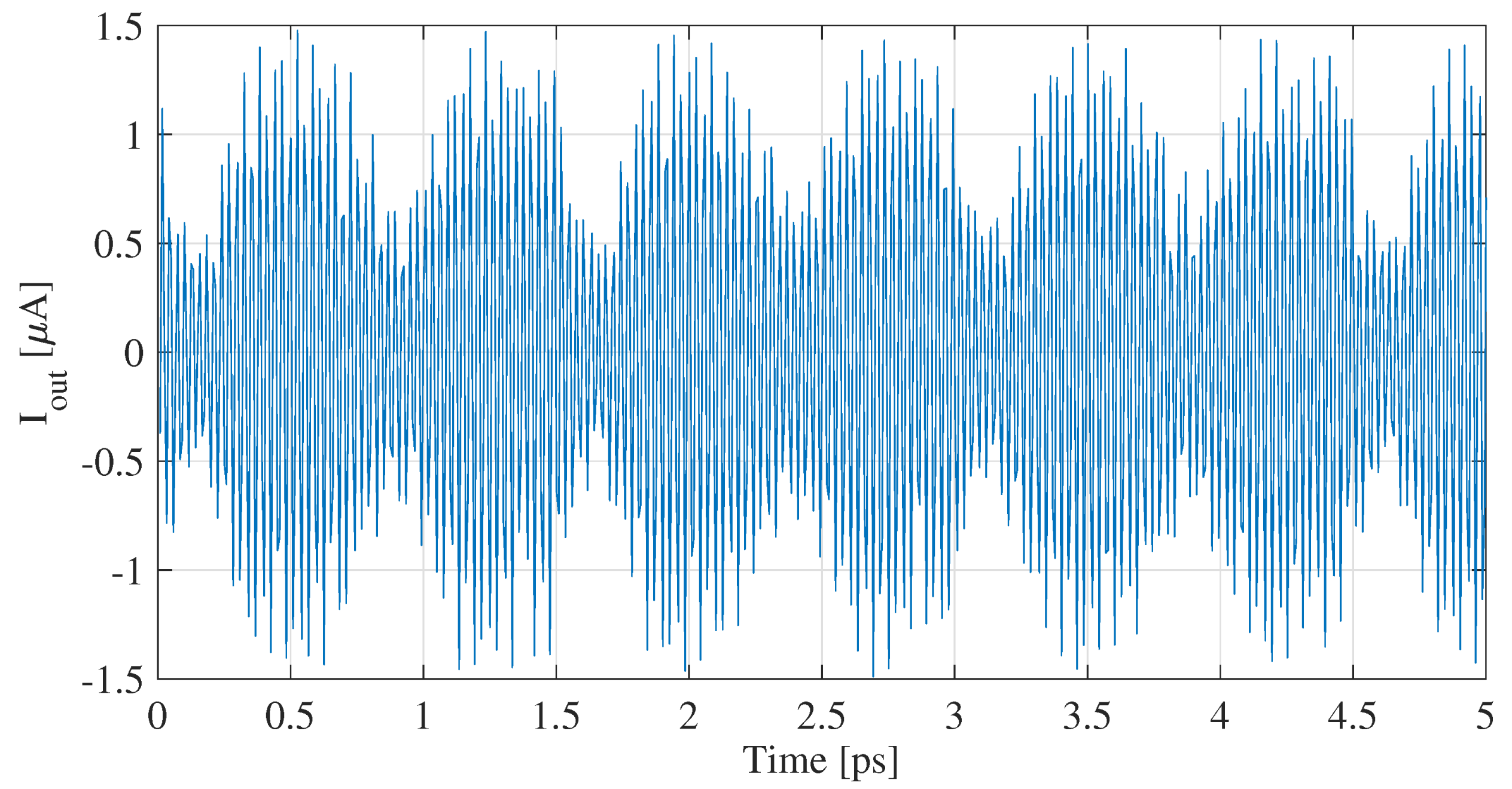
We begin with a detailed examination of the time-domain plot of the recorded current on the FET gate, as depicted in
Figure 4. This plot provides insights into the coupling efficiency of the plasmons from the graphene layer to the HMM gate. With minimal leakage confirmed from the simulations and a measured current in the
A range, a high coupling efficiency is ascertained.
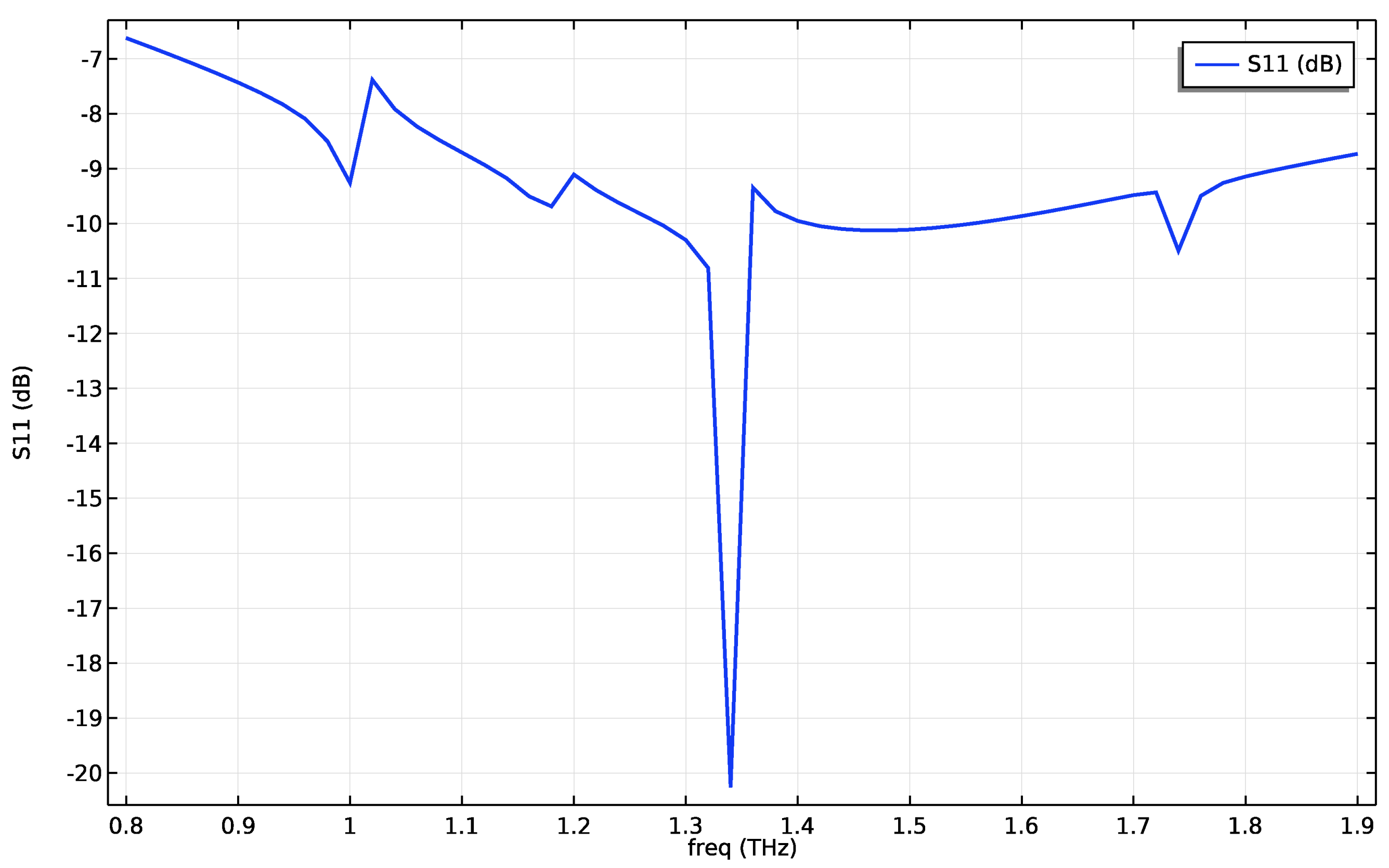
Next, we turn our attention to the S11 curve of the FET-antenna system, illustrated in
Figure 5. The S11 curve characterizes the reflection coefficient and, significantly, reveals the impedance matching capabilities of the antenna system. Notably, the S11 curve showcases minimal reflections at a frequency of 1.34672 THz, the resonant frequency of the current received from the FET, demonstrating optimal impedance matching and minimal power loss due to reflections.
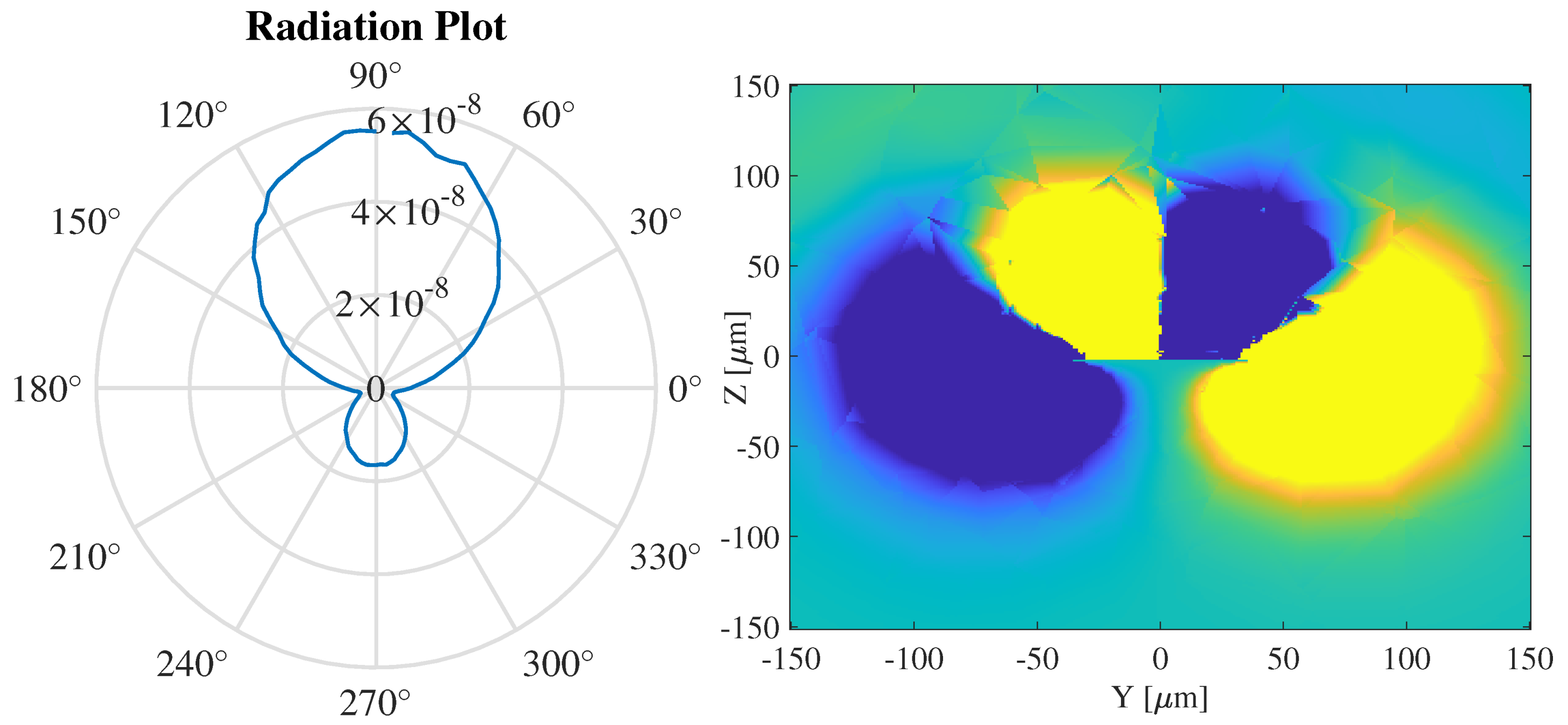
Regarding the radiative characteristics, we present the radiation pattern of the FET-antenna in
Figure 6(a) and the 2D EM field distribution via a 2D time-averaged Poynting vector in
Figure 6(b) with the
axis fixed at the center of the patch antenna. The 2D representation of the radiation pattern allows us to assess the antenna’s directivity, beamwidth, and angular distribution of radiated power. The simulations have yielded a directivity of
D = 52.7 dBi, with a radiative power of 2.2
W. For comparison, the detached asymmetric FET in [
9] without a bottom reflector or HMM provides 45 nW of radiative power. This large enhancement comes from the efficient coupling of the plasma waves to the gate, reducing the radiation efficiency of the stand-alone FET. The FET-antenna field plot, obtained from COMSOL and transferred to MATLAB, shows the field characteristics of the system in the transient interface with the current extracted from the FET. The microstrip patch antenna is centered on the
axis and the top of the antenna is aligned with
0.
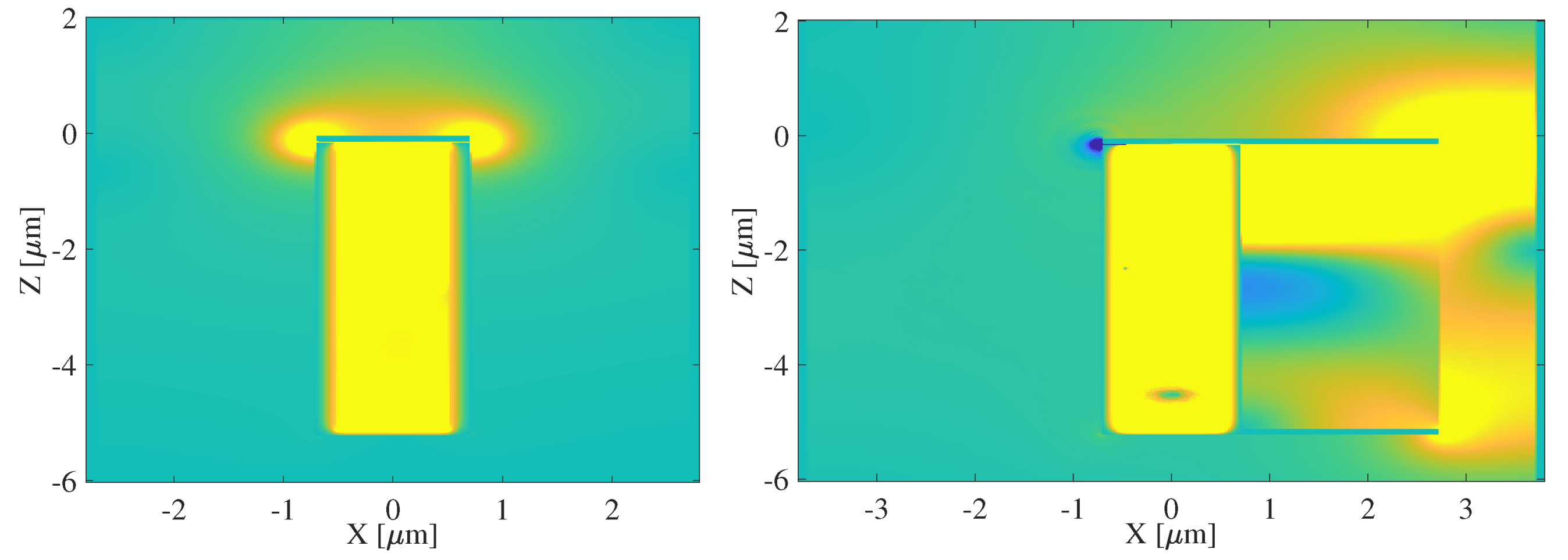
The 2D EM field distribution is analyzed using a time-averaged Poynting vector, first of the FET in
Figure 7(a) then of the FET-feed configuration in
Figure 7(b). The FET field plot, obtained from MATLAB with the device containing the metallic gate on the source side, HMM gate on the drain side, and the bottom reflector, confirms minimal leakage from the device to ensure maximum power transfer to the antenna. A small amount of radiative leakage is found at the top, where the boundary conditions required for the onset of the DS instability are sensitive, thus a small space between the gate and source/drain contacts are needed. The attached feed shown in
Figure 7(b) confirms the containment of the EM radiation within the FET for maximum power transfer to the feed. The small leakage is still observed on the source side of the FET, however the current and EM power are clearly transferred to the gate-feed extension.
The combined examination of these results offers a comprehensive understanding of the FET-antenna system, its resonance behavior, and its ability to efficiently radiate Terahertz signals at the resonant frequency.
5. Conclusions
In conclusion, our investigation of the microstrip patch antenna integrated with a graphene-based FET has revealed promising prospects for active Terahertz signal radiation. The FET’s charge transport dynamics and electrodynamics have been explored, leading to insights into transient behavior and power efficiency. Notably, our study identified a resonant frequency of 1.34672 THz, where the FET-antenna system exhibited optimal impedance matching and minimal reflections, making it a robust candidate for Terahertz signal generation.
The radiation pattern analysis of the FET-antenna showcased its favorable directional properties, highlighting its potential for applications in Terahertz communication, sensing, and imaging. The device’s high degree of tunability for impedance matching further underscores its versatility. Overall, this research provides valuable insights into the design and performance of Terahertz radiation systems, offering a promising path for advancements in this critical frequency range.
Author Contributions
Conceptualization, J.J., G.A., and J.C.; methodology, J.J., J.C., and X.R.; software, J.C. and X.R.; validation, J.J. and J.C.; formal analysis, J.C.; investigation, J.C.; resources, J.J.; data curation, J.C. and X.R.; writing—original draft preparation, J.C.; writing—review and editing, J.C.; visualization, J.C.; supervision, J.J. and G.A.; project administration, J.J. and G.A.; funding acquisition, J.J. All authors have read and agreed to the published version of the manuscript.
Funding
This work was partially supported by the Air Force Office of Scientific research (AFOSR) under Grant No. FA9550-16-1-0188 and the US National Science Foundation under Grant No. CNS-2011411.
Conflicts of Interest
The authors declare no conflict of interest. The funders had no role in the design of the study; in the collection, analyses, or interpretation of data; in the writing of the manuscript; or in the decision to publish the results.
References
- Oughton, E.J.; Lehr, W.; Katsaros, K.; Selinis, I.; Bubley, D.; Kusuma, J. Revisiting wireless internet connectivity: 5G vs Wi-Fi 6. Telecommunications Policy 2021, 45, 102127. [Google Scholar] [CrossRef]
- Akyildiz, I.F.; Han, C.; Hu, Z.; Nie, S.; Jornet, J.M. Terahertz band communication: An old problem revisited and research directions for the next decade. IEEE Transactions on Communications 2022, 70, 4250–4285. [Google Scholar] [CrossRef]
- Abadal, S.; Alarcón, E.; Cabellos-Aparicio, A.; Lemme, M.C.; Nemirovsky, M. Graphene-enabled wireless communication for massive multicore architectures. IEEE Communications Magazine 2013, 51, 137–143. [Google Scholar] [CrossRef]
- Akyildiz, I.F.; Jornet, J.M. Electromagnetic wireless nanosensor networks. Nano Communication Networks 2010, 1, 3–19. [Google Scholar] [CrossRef]
- Akyildiz, I.F.; Jornet, J.M. The internet of nano-things. IEEE Wireless Communications 2010, 17, 58–63. [Google Scholar] [CrossRef]
- Boubanga-Tombet, S.; Knap, W.; Yadav, D.; Satou, A.; But, D.B.; Popov, V.V.; Gorbenko, I.V.; Kachorovskii, V.; Otsuji, T. Room-temperature amplification of terahertz radiation by grating-gate graphene structures. Phys. Rev. X 2020, 10, 031004. [Google Scholar] [CrossRef]
- Dong, Y.; Xiong, L.; Phinney, I.; Sun, Z.; Jing, R.; McLeod, A.; Zhang, S.; Liu, S.; Ruta, F.; Gao, H.; others. Fizeau drag in graphene plasmonics. Nature 2021, 594, 513–516. [Google Scholar] [CrossRef] [PubMed]
- Crabb, J.; Cantos-Roman, X.; Jornet, J.M.; Aizin, G.R. Hydrodynamic theory of the Dyakonov-Shur instability in graphene transistors. Physical Review B 2021, 104, 155440. [Google Scholar] [CrossRef]
- Crabb, J.; Roman, X.C.; Jornet, J.; Aizin, G. Plasma instability in graphene field-effect transistors with a shifted gate. Applied Physics Letters 2022, 121. [Google Scholar] [CrossRef]
- Crabb, J.; Cantos-Roman, X.; Aizin, G.R.; Jornet, J.M. Amplitude and Frequency Modulation with an On-chip Graphene-based Plasmonic Terahertz Nanogenerator. IEEE Transactions on Nanotechnology 2022, 21, 539–546. [Google Scholar] [CrossRef]
- Jornet, J.M.; Akyildiz, I.F. Graphene-based nano-antennas for electromagnetic nanocommunications in the terahertz band. Proceedings of the Fourth European Conference on Antennas and Propagation. IEEE, 2010, pp. 1–5.
- Llatser Martí, I.; Kremers, C.; Chigrin, D.N.; Jornet Montaña, J.M.; Lemme, M.C.; Cabellos Aparicio, A.; Alarcón Cot, E.J. Radiation characteristics of tunable graphennas in the terahertz band. Radioengineering 2012, 21, 1–8. [Google Scholar]
- Jornet, J.M.; Akyildiz, I.F. Graphene-based plasmonic nano-antenna for terahertz band communication in nanonetworks. IEEE Journal on selected areas in communications 2013, 31, 685–694. [Google Scholar] [CrossRef]
- Llatser, I.; Kremers, C.; Cabellos-Aparicio, A.; Alarcón, E.; Chigrin, D.N. Comparison of the resonant frequency in graphene and metallic nano-antennas. AIP Conference Proceedings. American Institute of Physics, 2012, Vol. 1475, pp. 143–145.
- Llombart, N.; Chattopadhyay, G.; Skalare, A.; Mehdi, I. Novel terahertz antenna based on a silicon lens fed by a leaky wave enhanced waveguide. IEEE Transactions on Antennas and Propagation 2011, 59, 2160–2168. [Google Scholar] [CrossRef]
- Yurduseven, O.; Juan, N.L.; Neto, A. A dual-polarized leaky lens antenna for wideband focal plane arrays. IEEE Transactions on Antennas and Propagation 2016, 64, 3330–3337. [Google Scholar] [CrossRef]
- Tao, H.; Strikwerda, A.; Fan, K.; Padilla, W.J.; Zhang, X.; Averitt, R. Reconfigurable terahertz metamaterials. Physical review letters 2009, 103, 147401. [Google Scholar] [CrossRef] [PubMed]
- Jiang, X.Y.; Ye, J.S.; He, J.W.; Wang, X.K.; Hu, D.; Feng, S.F.; Kan, Q.; Zhang, Y. An ultrathin terahertz lens with axial long focal depth based on metasurfaces. Optics Express 2013, 21, 30030–30038. [Google Scholar] [CrossRef] [PubMed]
- He, Y.; Chen, Y.; Zhang, L.; Wong, S.W.; Chen, Z.N. An overview of terahertz antennas. China Communications 2020, 17, 124–165. [Google Scholar] [CrossRef]
- Peytavit, E.; Lampin, J.F.; Akalin, T.; Desplanque, L. Integrated terahertz TEM horn antenna. Electronics Letters 2007, 43, 1. [Google Scholar] [CrossRef]
- Dhillon, A.S.; Mittal, D.; Sidhu, E. THz rectangular microstrip patch antenna employing polyimide substrate for video rate imaging and homeland defence applications. Optik 2017, 144, 634–641. [Google Scholar] [CrossRef]
- Chahat, N.; Reck, T.J.; Jung-Kubiak, C.; Nguyen, T.; Sauleau, R.; Chattopadhyay, G. 1.9-THz multiflare angle horn optimization for space instruments. IEEE Transactions on Terahertz Science and Technology 2015, 5, 914–921. [Google Scholar] [CrossRef]
- Rebeiz, G.M. Millimeter-wave and terahertz integrated circuit antennas. Proceedings of the IEEE 1992, 80, 1748–1770. [Google Scholar] [CrossRef]
- Park, S.; Kim, C.; Jung, Y.; Lee, H.; Cho, D.; Lee, M. Gain enhancement of a microstrip patch antenna using a circularly periodic EBG structure and air layer. AEU-International Journal of Electronics and Communications 2010, 64, 607–613. [Google Scholar] [CrossRef]
- Barut, B.; Cantos-Roman, X.; Crabb, J.; Kwan, C.P.; Dixit, R.; Arabchigavkani, N.; Yin, S.; Nathawat, J.; He, K.; Randle, M.D.; others. Asymmetrically engineered nanoscale transistors for on-demand sourcing of terahertz plasmons. Nano Letters 2022, 22, 2674–2681. [Google Scholar] [CrossRef] [PubMed]
- Dyakonov, M.; Shur, M. Shallow water analogy for a ballistic field effect transistor: New mechanism of plasma wave generation by dc current. Phys. Rev. Lett. 1993, 71, 2465–2468. [Google Scholar] [CrossRef] [PubMed]
- Nafari, M.; Aizin, G.R.; Jornet, J.M. Plasmonic HEMT terahertz transmitter based on the Dyakonov-Shur instability: Performance analysis and impact of nonideal boundaries. Phys. Rev. Applied 2018, 10, 064025. [Google Scholar] [CrossRef]
- Mendl, C.B.; Polini, M.; Lucas, A. Coherent terahertz radiation from a nonlinear oscillator of viscous electrons. Appl. Phys. Lett. 2021, 118, 013105. [Google Scholar] [CrossRef]
- Cheremisin, M.; Samsonidze, G. D’yakonov-Shur instability in a ballistic field-effect transistor with a spatially nonuniform channel. Semiconductors 1999, 33, 578–585. [Google Scholar] [CrossRef]
- Knap, W.; Lusakowski, J.; Parenty, T.; Bollaert, S.; Cappy, A.; Popov, V.; Shur, M. Terahertz emission by plasma waves in 60 nm gate high electron mobility transistors. Appl. Phys. Lett. 2004, 84, 2331–2333. [Google Scholar] [CrossRef]
- El Fatimy, A.; Dyakonova, N.; Meziani, Y.; Otsuji, T.; Knap, W.; Vandenbrouk, S.; Madjour, K.; Théron, D.; Gaquiere, C.; Poisson, M.; others. AlGaN/GaN high electron mobility transistors as a voltage-tunable room temperature terahertz sources. J. Appl. Phys. 2010, 107, 024504. [Google Scholar] [CrossRef]
- Smith, D.; Schurig, D. Electromagnetic wave propagation in media with indefinite permittivity and permeability tensors. Physical Review Letters 2003, 90, 077405. [Google Scholar] [CrossRef]
- Zaitsev, A.; Demchenko, P.; Makarova, E.; Tukmakova, A.; Kablukova, N.; Asach, A.; Novotelnova, A.; Khodzitsky, M. Hyperbolic Bismuth–Dielectric Structure for Terahertz Photonics. physica status solidi (RRL)–Rapid Research Letters 2020, 14, 2000093. [Google Scholar] [CrossRef]
- Alekseyev, L.V.; Podolskiy, V.A.; Narimanov, E.E. Homogeneous Hyperbolic Systems for Terahertz and Far-Infrared Frequencies. Advances in OptoElectronics 2012. [Google Scholar] [CrossRef]
- Yang, X.; Yao, J.; Rho, J.; Yin, X.; Zhang, X. Experimental realization of three-dimensional indefinite cavities at the nanoscale with anomalous scaling laws. Nature Photonics 2012, 6, 450–454. [Google Scholar] [CrossRef]
- Liu, Z.; Lee, H.; Xiong, Y.; Sun, C.; Zhang, X. Far-field optical hyperlens magnifying sub-diffraction-limited objects. science 2007, 315, 1686–1686. [Google Scholar] [CrossRef]
- Rho, J.; Ye, Z.; Xiong, Y.; Yin, X.; Liu, Z.; Choi, H.; Bartal, G.; Zhang, X. Spherical hyperlens for two-dimensional sub-diffractional imaging at visible frequencies. Nature communications 2010, 1, 143. [Google Scholar] [CrossRef]
- Smith, D.R.; Schurig, D.; Mock, J.J.; Kolinko, P.; Rye, P. Partial focusing of radiation by a slab of indefinite media. Applied physics letters 2004, 84, 2244–2246. [Google Scholar] [CrossRef]
- Noginov, M.; Li, H.; Barnakov, Y.A.; Dryden, D.; Nataraj, G.; Zhu, G.; Bonner, C.; Mayy, M.; Jacob, Z.; Narimanov, E. Controlling spontaneous emission with metamaterials. Optics letters 2010, 35, 1863–1865. [Google Scholar] [CrossRef]
- Krishnamoorthy, H.N.; Jacob, Z.; Narimanov, E.; Kretzschmar, I.; Menon, V.M. Topological transitions in metamaterials. Science 2012, 336, 205–209. [Google Scholar] [CrossRef]
- Tumkur, T.; Zhu, G.; Black, P.; Barnakov, Y.A.; Bonner, C.; Noginov, M. Control of spontaneous emission in a volume of functionalized hyperbolic metamaterial. Applied Physics Letters 2011, 99. [Google Scholar] [CrossRef]
- Poddubny, A.; Iorsh, I.; Belov, P.; Kivshar, Y. Hyperbolic metamaterials. Nature photonics 2013, 7, 948–957. [Google Scholar] [CrossRef]
- Agranovich, V.; Kravtsov, V. Notes on crystal optics of superlattices. Solid State Communications 1985, 55, 85–90. [Google Scholar] [CrossRef]
|
Disclaimer/Publisher’s Note: The statements, opinions and data contained in all publications are solely those of the individual author(s) and contributor(s) and not of MDPI and/or the editor(s). MDPI and/or the editor(s) disclaim responsibility for any injury to people or property resulting from any ideas, methods, instructions or products referred to in the content. |
© 2023 by the authors. Licensee MDPI, Basel, Switzerland. This article is an open access article distributed under the terms and conditions of the Creative Commons Attribution (CC BY) license (http://creativecommons.org/licenses/by/4.0/).
