1. Introduction
With the increase in power and operational capabilities of systems as well as the miniaturization of hardware dimensions, the complementary metal-oxide-semiconductor (CMOS) technology has faced serious problems. As a result, researchers in this field have sought to find ways to improve power consumption and circuit area. The use of GDI as a method for improving power and area utilization has been proven due to its use of fewer transistors and minimal power loss compared to CMOS technology. The simplest GDI circuit is created by connecting two PMOS and NMOS transistors, in which the source terminals of the N-type and P-type transistors are connected to "P" and "N" inputs instead of being connected to ground or supply voltage [
1]. Each of the P, N, and D terminals in the GDI method may be used as both input and output depending on the circuit structure. The structure of the GDI cell has a basis similar to the CMOS inverter structure. Various binary functions can be implemented in GDI using only two transistors, whereas other techniques require the use of 6 to 12 transistors for each of these functions [1, 2]. The advantages of GDI over CMOS include the use of fewer transistors, faster speed, less power loss, and reduced complexity in Boolean functions. Multiple GDIs can also be connected for designing multi-input gates [
3]. Although GDI-based digital integrated circuits have their advantages, such as low power consumption and simplified designs, they do have a drawback in that they lack the ability to achieve a full-swing capability, so Ref. [
4] has combined dynamic logic style and GDI to achieve full-swing capability.
With nanoscale circuit design, the use of alternative technologies is necessary more than ever. As a transistorless technology, QCA is a candidate technology to replace CMOS technology with lower power consumption and higher speed. In this technology, the physical simulation of automata is done using quantum point cells [
5]. This technology offers low energy consumption, high-speed switching, and very small dimensions by integrating Boolean logic and Coupled Quantum Dot characteristics [
6]. In this logic, binary information is transmitted based on the coulombic repulsion between adjacent cells, solving the problems caused by wired connections between transistors, which was a major issue in CMOS technology. Furthermore, by placing electrons in quantum points of cells, binary values of 0 or 1 are encoded [
7]. Finally, it can be said that compared to CMOS, QCA can implement very large-scale integration (VLSI) architecture with much lower energy consumption and higher speed at the nanoscale [
5].
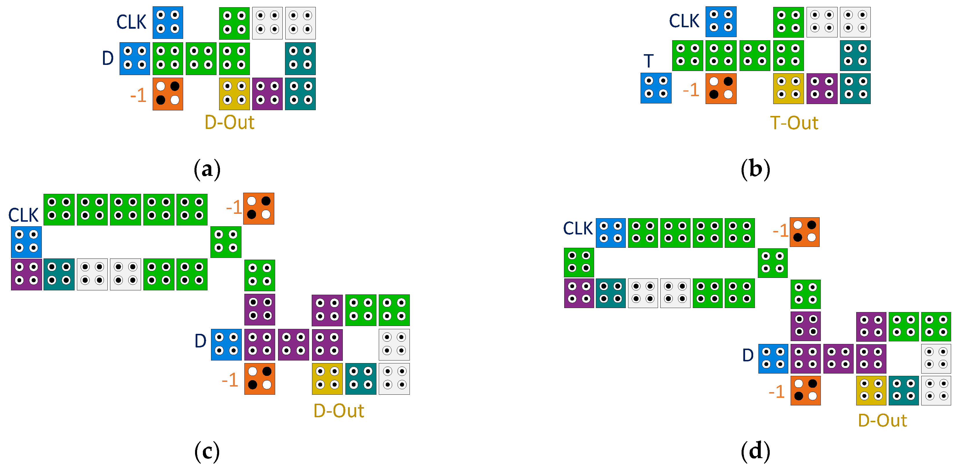
The objective of this paper is to introduce an optimized GDI block based on QCA as a standard design unit capable of performing basic functions for implementing a wide range of digital combinational and sequential circuits. Given the challenges posed by existing design methodologies and taking into account the comprehensiveness of the design and the multitude of executable functions of the proposed block, it can serve as a novel design logic. Additionally, by interconnecting several of these proposed blocks as fundamental gates, it becomes feasible to design more intricate combinational and sequential circuits. For instance, within this paper, a four-bit parity circuit and a single-bit memory are both designed and subjected to simulation through the combination of two of these proposed blocks.
The organization of the article is as described below:
Section 2 Gives a summary of the QCA technology used in digital design. The proposed QCA-MGDI block is designed, simulated, and evaluated in
Section 3.
Section 4 presents the designed combinational circuits using the proposed MGDI-QCA block and their simulation and evaluation results. In
Section 5, several sequential circuits are designed using the proposed block. The conclusion is presented in
Section 6, followed by a comparison of the results with some previous works in Section 7 and a conclusion.
2. An overview of QCA-based circuits
Circuits in QCA technology consist of several QCA cells. Inside every cell, there are four dots and two extra electrons. These electrons freely move inside the cell. The placement of these electrons on either of the two main diagonals of the cell creates a logical charge of 0 or 1. In this method, the charge level of each cell is determined based on the susceptibility to the Coulomb force between the four adjacent cells, the four diagonal cells on all four sides, and the upper- and lower-layer cells. Therefore, to determine the charge of each cell, it is necessary to determine the charge of the adjacent cells[
5] . In
Figure 1, a quantum cell is depicted in two polarization states of 0 and 1.
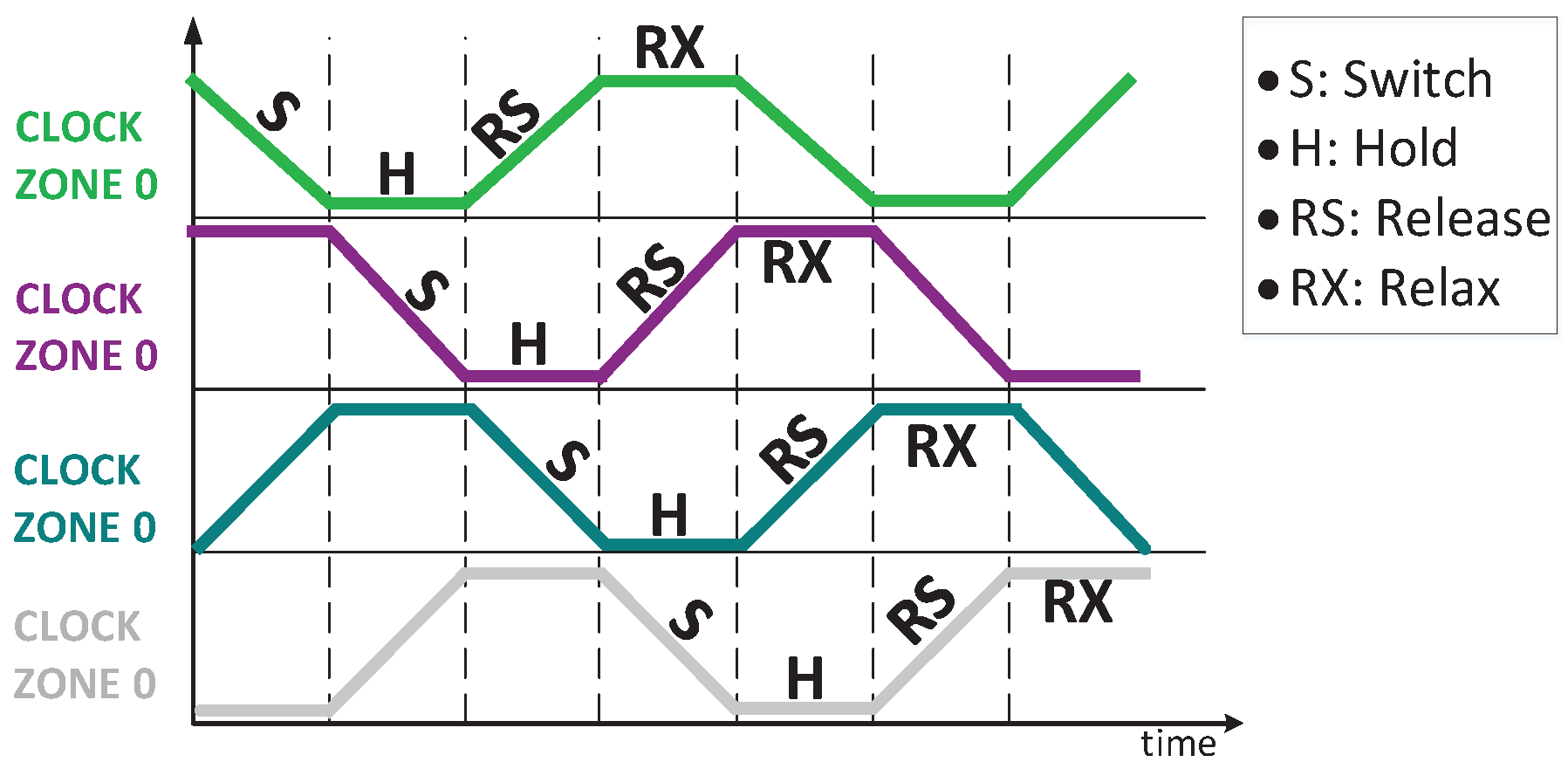
Clock zone in QCA technology, in addition to controlling data flow, also supplies energy to cells. As it is shown in
Figure 2, this structure in QCA consists of four zones: 0, 1, 2, and 3, each zone formed by four distinct clock phases as shown in
Figure 2. These phases include: switch, hold, release, and relax [
8]. The polarization of each cell is determined in the switch state. Then, the polarization determined in the hold stage remains constant. In the release stage, the polarization of the cell is gradually reduced, and in the relax stage, the polarization of the cell disappears completely [
9].
If
is the energy of the kink between two cells a and b, this energy is related to the energy of two cells with opposite polarization. The total circuit energy is calculated based on equation (1), where the
is the polarization of cell b. Also,
is the electron tunneling energy inside cell a. Sigma is applied to all cells that are in the effective radius from cell a, which is usually determined before simulation. In equation (2),
is the polarization state of the cell, and
is the polarization of the neighboring cell. Using this function, the simulation engine calculates the state of each cell using the other cells that are within the effective radius. This calculation is repeated with a pre-determined tolerance until the entire system converges.
To investigate the energy level and determine the polarization of dynamic circuits, simulation is performed using the correlation vector engine. The kink energy indicates the amount of energy of cells a and b with opposite polarization. One can readily determine the amount of energy by evaluating the electrostatic interaction among all charges [
15]. To achieve this objective, the electrostatic interaction between each point in cell a and a different point within the same cell is computed by utilizing equation (3). In this equation, the constant of proportionality k is called Coulomb's constant.
To calculate the kink energy, first this energy is calculated for cells with opposite polarity and then for cells with the same polarity, and these two values are subtracted from each other. Since the cell charge is neutral, the interaction between cells decreases through the quadrupole-quadrupole interaction with the inverse ratio of the fifth power of the distance between them. Therefore, the kink energy rapidly decreases with increasing distance and effective neighbor radius.
Types of cells in QCA include simple cells and rotated cells. By placing multiple simple cells next to each other, a 90◦ wire is created. In this wire, the input polarization is transferred to the adjacent cells without changing until the end of the wire. By using rotated cells, a 45◦ wire is created, where the complementary polarization of the input is transferred to the adjacent cell, and this process continues to the end of the wire. For this reason, this wire is also called an inverter chain [10, 11].
Additionally, there are two design methods for designing crossover wires, namely the coplanar and multilayer methods. In the coplanar method, to allow crossover wires to pass over two perpendicular wires, one wire of the 45◦ type and another of the 90◦ type are used. In this method, cross-coupling effects are created in the crossover wires due to the displacement and inconsistency of cells. To overcome this challenge and increase circuit robustness, some work has been done, which has led to an increase in circuit area and overhead [
12]. The first method involves the crossover of wires based on different clock phases, which has less overhead cost compared to other methods [
12]. In this method, two-phase cells (switch and release), as well as two-phase cells (hold and relax) can pass over each other without the effect of destructive polarization. The second method, called the multilayer method, uses multiple layers for design. In both methods, crossed cells are not interacting with each other [
13].
The 3-input majority gate and the inverter gate are two basic gates in QCA technology. They can be used to simulate AND & OR gates, and combined with the inverter gate, they can be used to create other combinational and sequential circuits. However, the main challenge with this design method is the increase in delay and circuit area, due to the large number of gates and the need for internal connections between them [
14]. The use of more comprehensive gates, which can perform more operations than the majority and inverter gates, can reduce the area, power consumption, and delay [
6].
On the other hand, in QCA technology, the set of design rules, timing constraints, and layering considerations encompass specific geometric and connectivity limitations that ensure performance reliability and circuit sensitivity reduction [
15]. These rules define the minimum and maximum number of cells in a clock zone or the synchronization of input currents to a gate. Accordingly, each QCA clock zone must consist of at least two cells to maintain its influence in the subsequent clock zone. As per timing law, all input signals of a specific gate must be set in the same timing zone and prior to the clock zone of that gate. Similarly, the output wire connected to the next gate must reside in a clock zone after the intermediate cells. This structure guarantees the transmission of polarized signals [
15,
16,
17]. Another design guideline in the QCA structure involves prioritizing the implementation of gates like mux and xor over general gates like majority and not gates. In order to simplify the functions, first, as much as possible, the simplification is done with the help of higher priority gates in order to use fewer basic gates, consequently reducing area, delay, and power consumption [
18].
As described in the [
19], the linear synthesis tool is given as input to the Layout Generator. By reading the logical inputs and circuit expansion, this set detects the placement of the gates and finally draws the gates and describes the input signals. Finally, the output layout is delivered to QCADesigner so that the design can be done automatically. It's worth mentioning that the aforementioned process pertains to combinational circuits and does not address the development of the place and route tool. In the reference by [
18], the circuit is divided into primary and secondary level blocks. In the primary phase, blocks are divided into cell and gate levels. The design is carried out using two methods: canonical and evaluation. The interconnecting wires are selected. If the design has been performed with clock application, both categories of primary and secondary level blocks are instantiated. By establishing connections and applying the clock, the design concludes. In this article, a circuit design approach based on the proposed blocks is also presented in Section4.
Using optimization methods to design circuits involves using successful methods from other technologies in the target technology. For example, in reference [
4], a combination of GDI and dynamic logic called D-GDI is proposed for designing dynamic XOR cells and ultimately full adders. This method significantly reduces the area, Power Delay Product (PDP), and the parasitic capacitances connected to the output node and other intermediate nodes. Additionally, the D-GDI full adder circuit has reduced power consumption by 20% compared to the best available sample. In reference [
20] and in an improved version of this cell, the chip area for pull-up and pull-down networks is reduced by approximately 80% and 50%, respectively, compared to the basic GDI cell. Moreover, the PDP of this cell is also improved.
In [
1], based on the circuit proposed in reference [
20], a GDI block is designed in QCA technology. This block uses 16 QCA cells to implement seven functions. The area of the QCA-GDI block is 0.02 um2 and its delay is 2 clock pulses. Additionally, in this work, using the QCA-GDI cell, MUX circuits with two and four inputs were designed and simulated; these circuits include respectively 16 and 30 cells with an average energy of 29.66 µeV. A two-input XOR with 39 cells, a delay of 2 clock phases, and an energy of 44.48 µeV was also designed and implemented. A full-wave rectifier (FWR) was designed and simulated with 30 cells and a delay of 2 clock phases. This block also has a high number of cells and a large area, but the low delay and the accessibility of input and output cells are the advantages of this method.
In reference [
21], a three-input Universal Logic Gate (ULG) has been designed in QCA technology. This gate is "planar" and capable of implementing AND, OR, and XOR gates. The area of the block with 11 cells is 0.01 um2 and it operates in 1 clock phase. Although the reduction in the cell number, small area, and very low delay are advantages of the proposed method, the low robustness and small number of operations are its disadvantages.
In reference [
22], a 30-cell universal gate with 6 input cells has been designed. This block, designed in 3 layers, implements 13 standard universal gate functions. An area of 0.11 um2 is one of its disadvantages, indicating a large number of cells. However, a delay of 1 clock phase and the accessibility of input and output cells are advantages of this method.
In [
23], according to the suggested approach in [
24], the design of several basic circuits, adders, and comparators has been implemented in QCA technology. In this reference, an XOR gate with 11 cells in two clock phases and an area of 0.012 um2 and a MUX gate with 19 cells and an area of 0.02 um2 are designed. Also, the proposed adder circuit in this work with 73 cells and an area of 0.08 um2 and the single-bit comparator circuit with 25 cells and an area of 0.03 um2 are designed and simulated. The advantage of this method is the low delay in the designed circuits and gates. The use of various structures in the design, large number of cells, and high area are the disadvantages of this approach.
In [
25], a QCA-based GDI block using 11 cells is presented. The area of the block is equal to 0.01 um2 and its delay is one clock phase. This block is based on the majority function according to equation (4). Using the presented block, nine basic functions are executed.
However, using the GDI method in designing a universal gate in QCA technology can reduce power consumption and lead to a reduction in the area of the circuits designed with this method, due to the unnecessary use of basic gates. Therefore, this article aims is to propose a new QCA-based MGDI block as a standard design unit for designing basic functions for implementing various digital circuits, in such a way that for the first time, the standard 4-input block is employed to mitigate circuit complexity and reduce area occupancy. Ultimately, the proposed design exhibits a 19% decrease in cell count, a 29% reduction in total wasted energy, an increase in the number of implementable functions to 21 (compared to the conventional GDI technique's 6 functions), and a 44% decrease in average energy dissipation at the same level of occupancy. As indicated in
Table 2, certain functions can be implemented using various combinations of inputs, enhancing the design's flexibility. Additionally, the designed GDI block is incorporated into multiple combinational and sequential circuits to verify its operational accuracy.
3. Proposed MGDI-QCA block
One of the feasibility assessment methods for optimizing circuits is pattern recognition from optimization techniques used in other technologies and simulating them in the target technology. It is known that the GDI technique is one of the methods for improving energy efficiency and reducing area occupancy in CMOS technology. Using this technique, various binary functions can be implemented with the least number of transistors, resulting in a 60 to 80 percent saving in area for basic gate designs [
26]. In
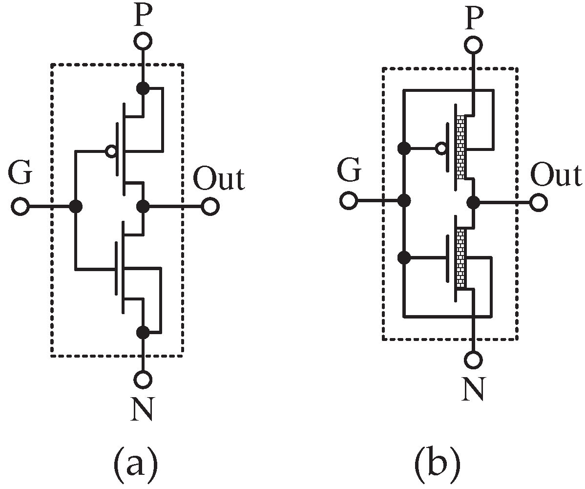
Figure 3-a, a basic GDI cell with 4 terminals is shown, and in
Figure 3-b, an enhanced GDI is observed.
Table 1 illustrates different Boolean functions that can be generated using this block[
1]. Furthermore, for designing multi-input gates, multiple GDIs can be interconnected[
1].
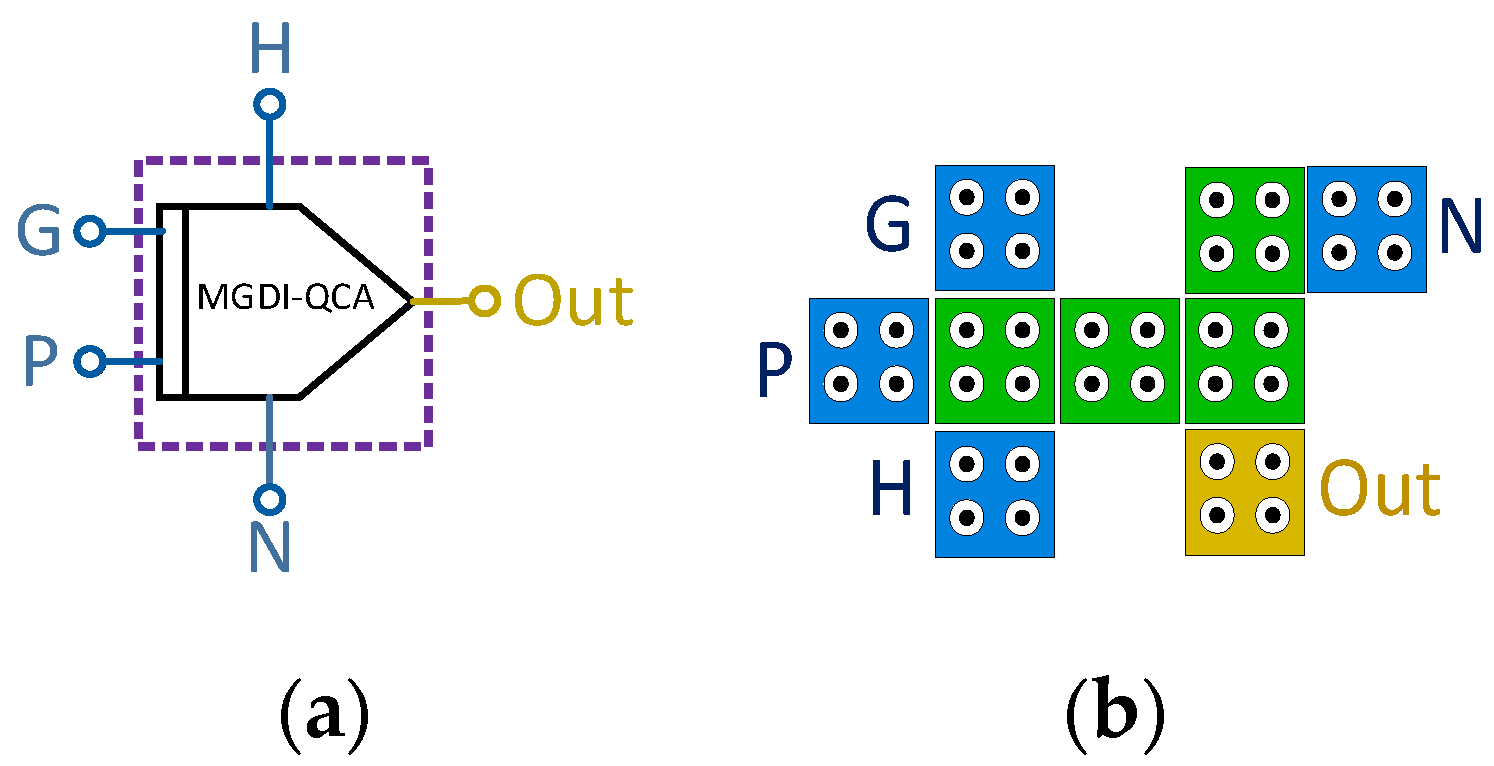
In this article, first by modifying the GDI structure, a four-input GDI called Modified GDI (MGDI) is designed, and then the resulting MGDI is simulated in QCA technology. The proposed MGDI-QCA block, as shown in
Figure 4, consists of 9 cells, including four input terminals (P, G, N, and H) and one output cell. The features of the proposed architecture include single-layer design and the avoidance of cross-coupling methods, as these methods lead to increased noise and area occupancy. Furthermore, designing the proposed cell in a single clock phase has resulted in an optimally delayed circuit. Subsequently, while adhering to design rules and principles of clocking, along with proper positioning of each input and output terminal of the proposed block, simulation of the proposed block has been conducted, and the consumed energy has been calculated. In this context, QCADesigner-E version 2.0.3 has been utilized in the 18-nanometer technology, employing default simulation parameters as per
Table 3 and utilizing simulation engines such as dual vector and coherence vector.
The equation for the proposed MGDI-QCA block is presented in equation (5), which is written based on its Karnaugh map and its simplification.
As shown in
Table 2,the significant increase in the number of output modes of the proposed block compared to the standard mode is the result of proper arrangement for adding an additional input.
Table 2.
Logic functions implemented by the proposed MGDI cell.
Table 2.
Logic functions implemented by the proposed MGDI cell.
| H |
N |
P |
G |
OUT |
|
H |
N |
P |
G |
OUT |
| 0 |
0 |
B |
A |
AND (A, B) |
|
0 |
B |
A |
1 |
A |
| 1 |
B |
0 |
A |
|
1 |
B |
A |
0 |
| B |
A |
0 |
1 |
|
1 |
B |
A |
1 |
B |
| 1 |
1 |
B |
A |
OR (A, B) |
|
0 |
B |
A |
0 |
| 0 |
B |
1 |
A |
|
0 |
1 |
B |
A |
B+A' |
| B |
A |
1 |
0 |
|
1 |
B |
1 |
A |
| -1 |
-1 |
1 |
A |
Buffer(A) |
|
B |
A |
1 |
1 |
A+B’ |
| -1 |
1 |
-1 |
A |
NOT(A) |
|
1 |
0 |
B |
A |
A'B |
| B |
C |
- |
A |
Maj (A, B, C) |
|
0 |
B |
0 |
A |
| 0 |
C |
B |
A |
MUX=A’C+AB |
|
B |
A |
0 |
0 |
AB’ |
| 1 |
C |
B |
A |
MUX=A’B+AC |
|
B |
0 |
0 |
A |
0 |
| C |
B |
A |
0 |
MUX=AC+BC’ |
|
B |
1 |
1 |
A |
1 |
| C |
B |
A |
1 |
MUX=BC+AC’ |
|
B |
A |
0 |
C |
AB’C’+ABC |
| B |
0 |
1 |
A |
XOR (A, B) |
|
B |
A |
1 |
C |
A+B’C+BC’ |
| B |
1 |
0 |
A |
XNOR (A, B) |
|
A |
0 |
C |
B |
AB’C+A’BC |
| A |
C’ |
C |
B |
TIEO (A, B, C) |
|
A |
1 |
C |
B |
A’+C+B’ |
| B |
A |
A’ |
C |
|
|
|
|
|
|
Table 3.
This is a table. Tables should be placed in the main text near to the first time they are cited.
Table 3.
This is a table. Tables should be placed in the main text near to the first time they are cited.
| Parameter |
Value |
Parameter |
Value |
| Cell size |
18 nm*18 nm |
Relative permittivity |
12.9 |
| Dot diameter |
5 nm |
Clock high |
9.8 e-022J |
| Cell-to-cell spacing |
2.9 nm |
Clock low |
3.8 e-023J |
| Number of samples |
12800 |
Clock shift |
0.0e+000 |
| Convergence tolerance |
0.001 |
Clock amplitude factor |
2 |
| Radius of effect |
41 nm |
Layer separation |
11.5 nm |
| Maximum iterations per sample |
100 |
|
|
In
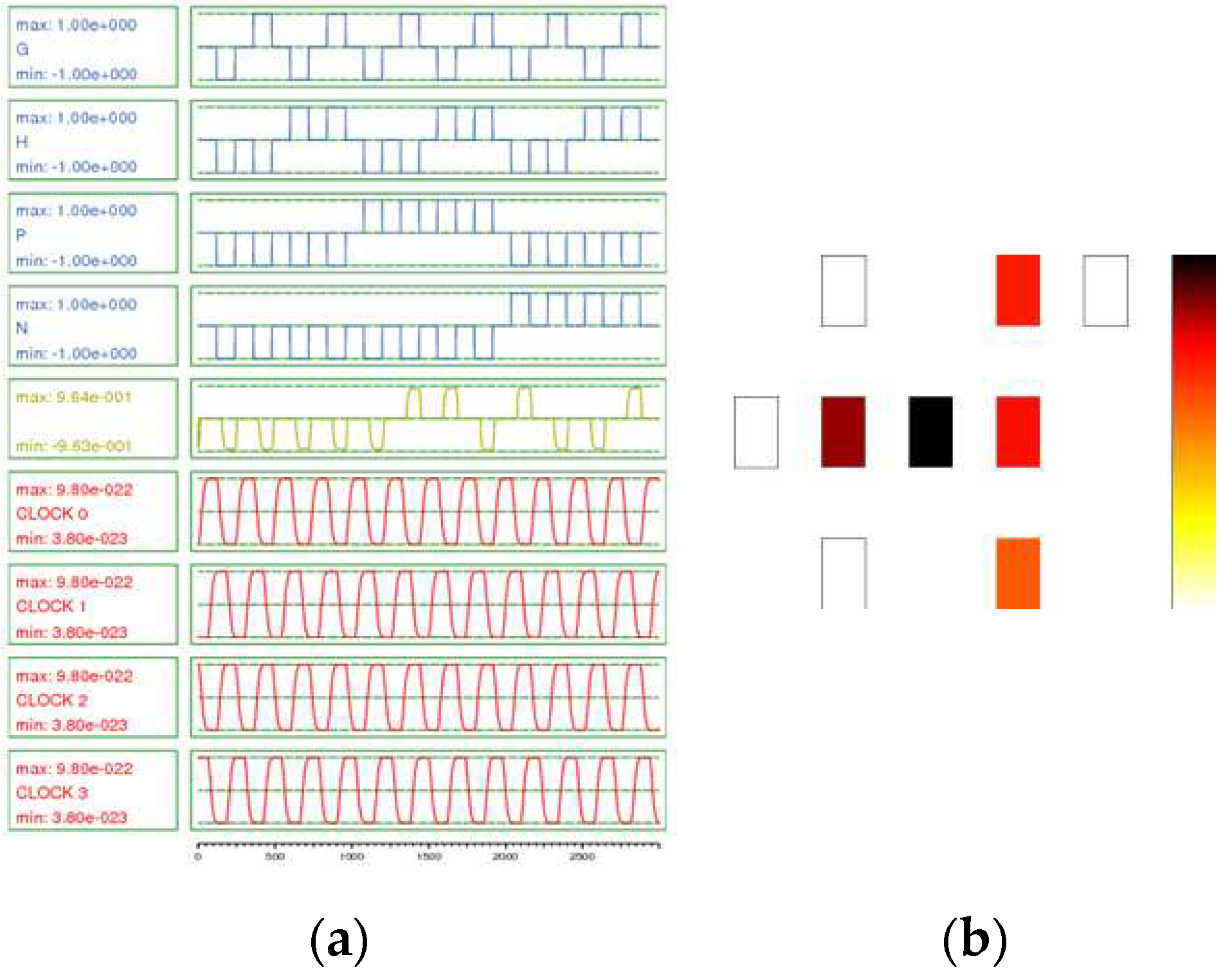
Figure 5, the energy consumption distribution map and the analysis of the block's operation (including output states for various inputs and different clock phases) using QCAPro simulator are depicted. It is evident that from a logical perspective, the performance validity of the block is confirmed in all cases
Table 4 provides the consumed energy of the proposed block at three energy levels, calculated and presented according to the method proposed in [
27]. Clearly, the static energy stemming from leakage power is significantly lower than the dynamic energy arising from switching, displaying a similar state to circuits of CMOS technology. The Avg Energy Dissipation of the circuit, represented by Ebath_total, is estimated as the sum (Ebath) for each clock pulse cycle by each cell in the design, aiming to illustrate the overall wasted energy.
4. Designed combinational circuits using the proposed MGDI-QCA block
As shown in
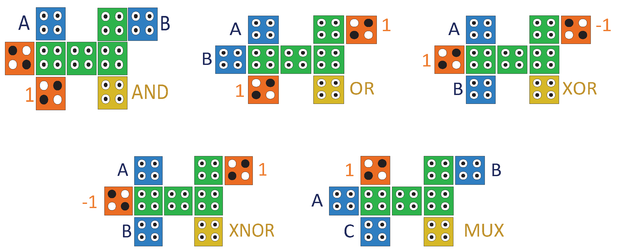
Table 2, by using the proposed block and only with a different value from the unit structure of the proposed block, various basic functions (such as AND, OR, NOT, BUFFER, XOR, XNOR, MUX, Majority, and three input Exclusive OR) can be implemented. For example, according to equation (6), by setting the values of A, -1, B and -1 to the outputs of gates G, P, N, and H, respectively, the AND gate can be obtained.Additionally, equation (7) represents the OR gate, which is generated by assigning values A, 1, B, and -1 to input terminals. Similarly, for constructing the XOR gate, values A, 1, 0, and B are placed at the input terminals, according to equation (8). Equation (9) expresses the XNOR gate. To create this gate, input terminals G, P, N, and H are respectively assigned values A, -1, 1, and B.
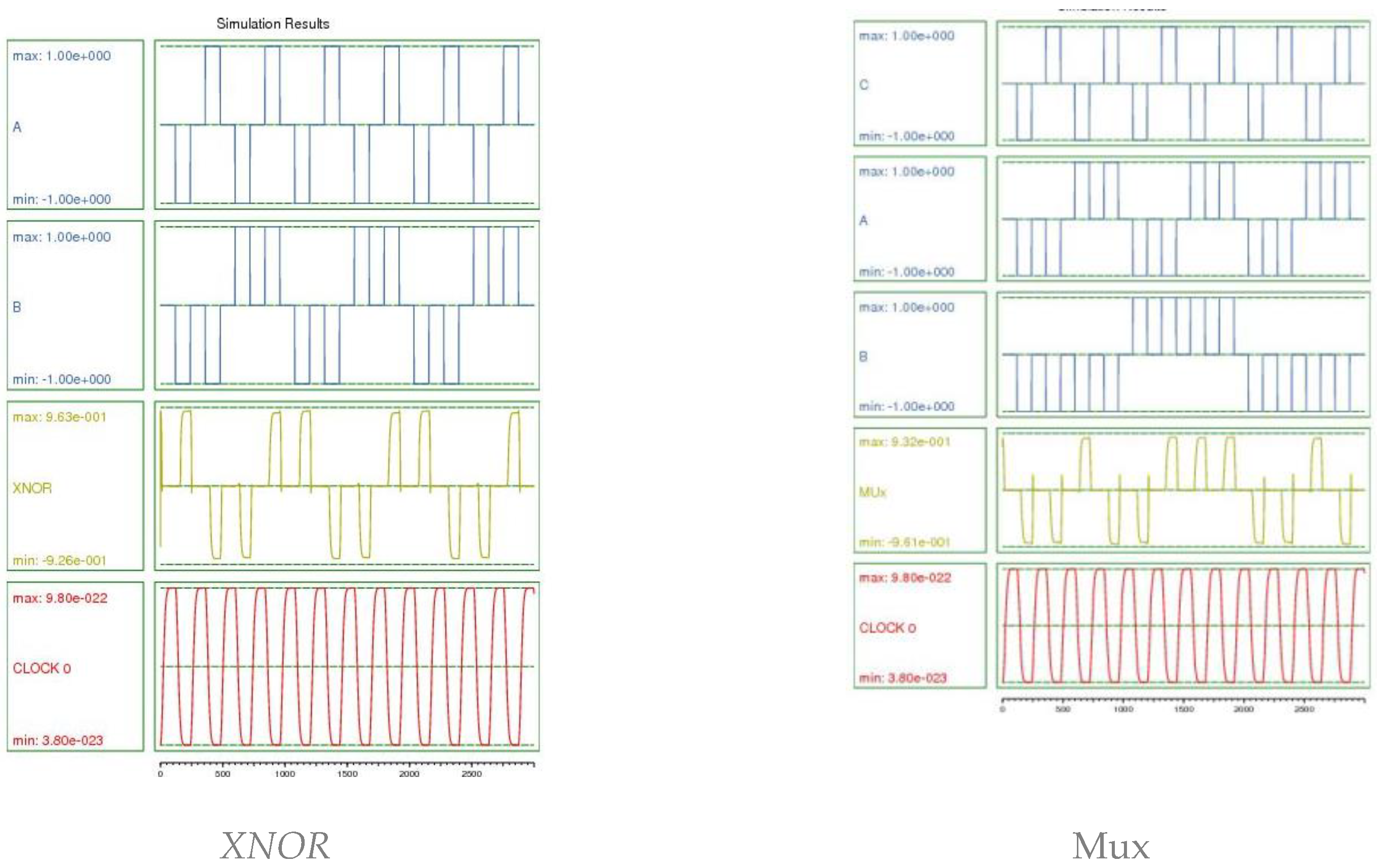
Figure 6 illustrates the design of some basic gates using the proposed block. The simulation results of two examples are shown in
Figure 7. The results demonstrate the correctness of the logical operation of the proposed gates design and the flexibility of the proposed block in designing combinational circuits.
In addition to the mentioned basic gates, by connecting multiple proposed blocks, more complex combinational and sequential circuits can be designed. As outlined in the design flowchart in
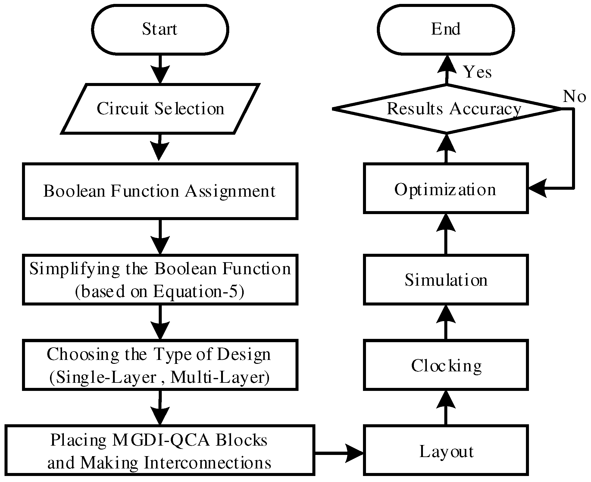
Figure 8, to design various circuits using the proposed block, after selecting the desired circuit and writing its logical function, simplification is performed based on Equation (5). Then, by choosing the design type (multi-layer or single layer) and adhering to design and scheduling rules, the placement of the proposed block and the combination of blocks are carried out. After simulation and result analysis, the design and simulation steps are repeated until reaching the optimal state.
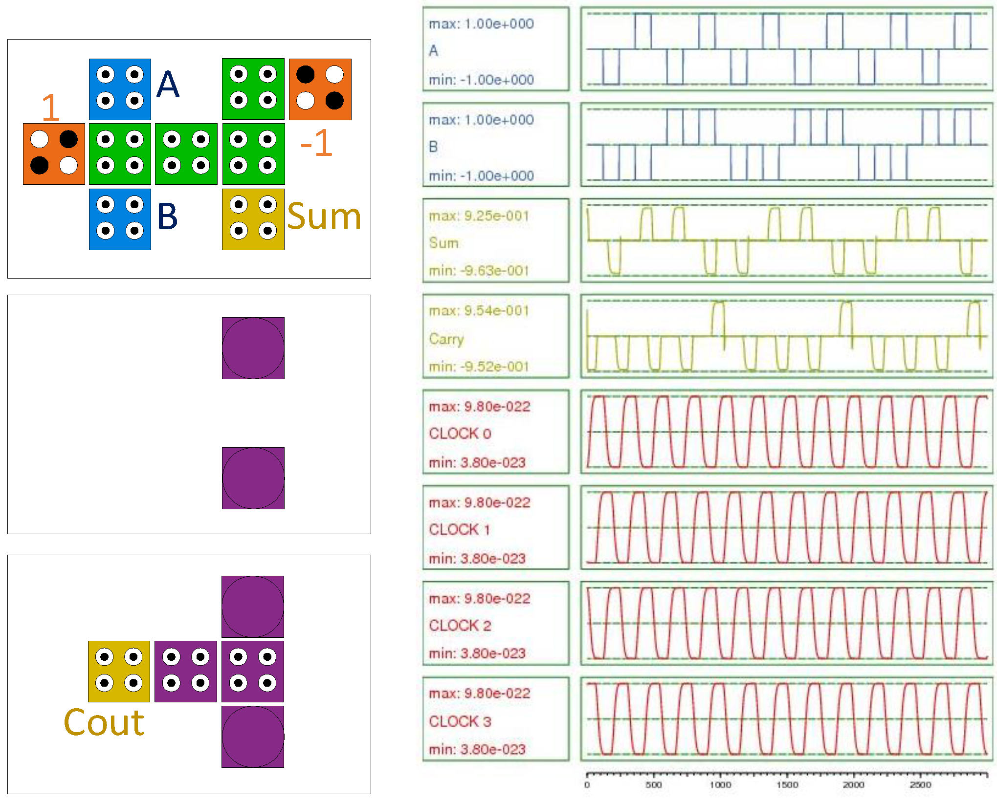
Figure 9 illustrates a three-layer proposed basic half-adder circuit, which consists of an XOR gate for computing the Sum bit and an AND gate for computing the Carry bit.
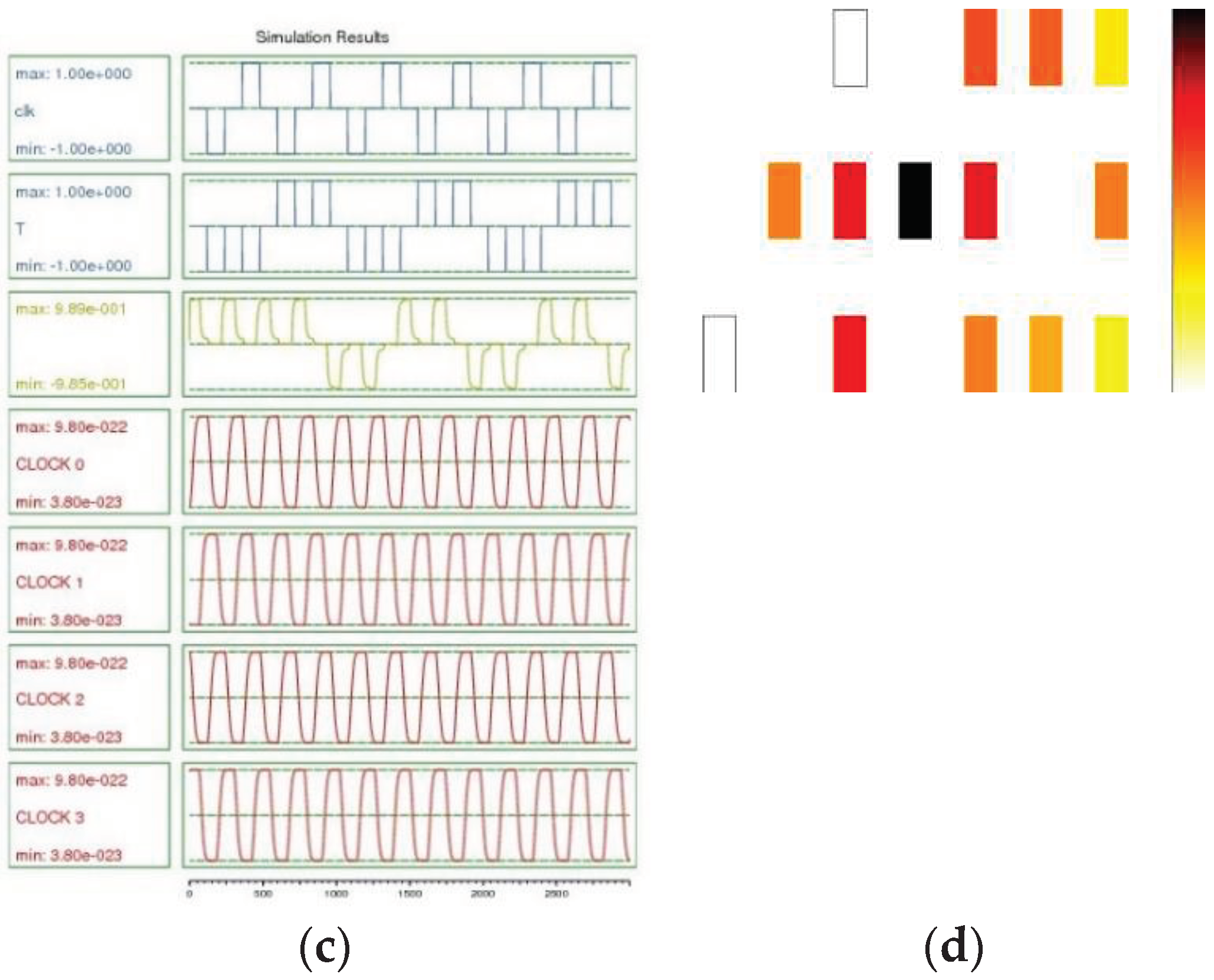
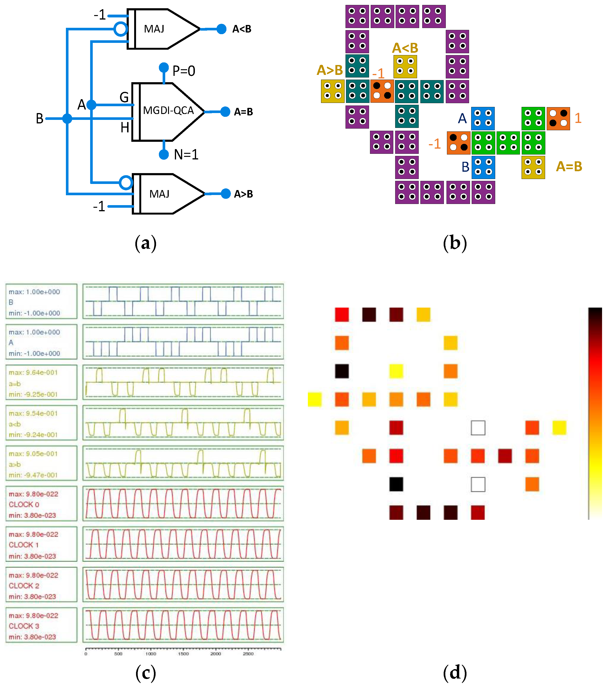
Using the proposed MGDI-QCA block, a single-bit comparator on a single layer, along with its structure, circuit, simulation results, and energy levels, is shown in
Figure 10. The same aspects are also illustrated as an example of a four-bit parity generator circuit in
Figure 11.
We know that quantum coherence transmitting electric fields can lead to noise interference when implemented at small distances. This asymmetry results in the creation of hidden noisy paths within the structure. Furthermore, this phenomenon becomes apparent in the separation of desired and undesired signals. Since QCA cells are linear, they exert a two-phase influence on neighboring cells; a small change in the polarity of one cell leads to a larger change in an adjacent non-polar cell, causing simultaneous reinforcement of both desired and undesired signals. The existing positive feedback leads to stronger polarity and signal injection[
28]. However, as also mentioned in[
13], this effect is more pronounced in multi-layer circuits and, in general, is neglected in previous works due to the lack of an appropriate noise model in QCA and the suitability of the transmitted signal shape. In this paper, due to adherence to design rules and appropriate clocking of the designed structure, as seen in
Figure 5,
Figure 7,
Figure 9,
Figure 10,
Figure 11 and
Figure 13 the responses appear acceptable. This observation is evident in the comparison of outputs with previous works, under the same software and identical conditions.
5. Comparison
In this section, the results of the proposed design are compared with some previous works. Also, the sequential and combinational circuits designed by the proposed block are compared with previous similar circuits in terms of parameters such as area, delay and quantum cost. For this purpose, the proposed circuit simulations have been performed using the 2.0.3 version of QCADesigner-E in 18-nanometer technology. Accordingly, simulation engines such as dual vector and coherence vector have been used to determine the polarization of the cells with default simulation parameters. Similar results were obtained using both simulation engines, indicating the accuracy of the proposed design. According to the comparison in
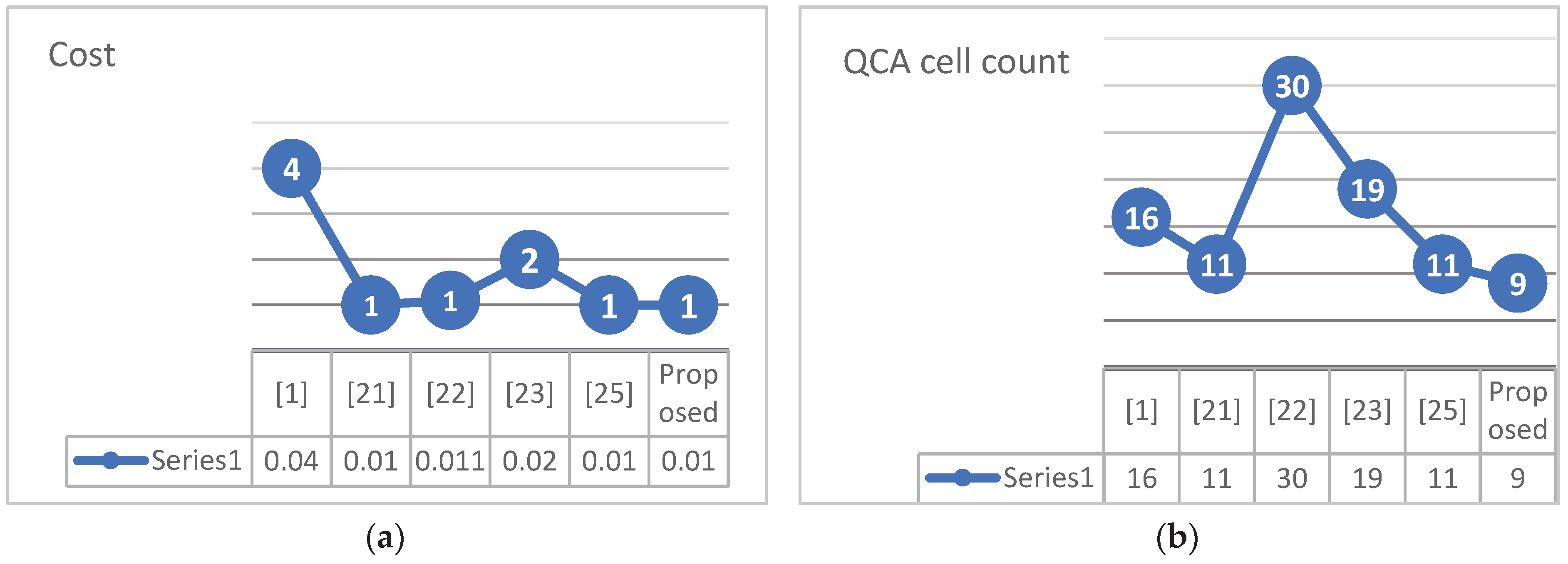
Table 5, the proposed MGDI-QCA block is better than all previous works in terms of the number of cells. It also has advantages in terms of area and delay compared to previous works, such that if the product of area occupation and delay is defined as the cost function, only references [
21] and [
25] have a similar cost, while the circuit in reference [
21] is of the coplanar type and the circuit in reference [
25] has 11 cells. These details are also shown in the vector graphs in
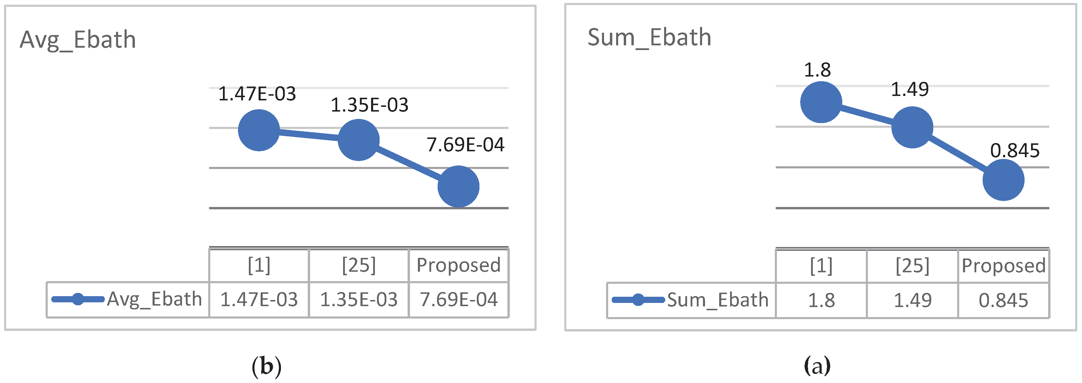
Figure 15. The energy consumption of the proposed design has been examined using QCAPro as given in
Table 6. The results indicate an energy consumption close to half that of other works. Additionally, the results of evaluating the total and average dissipated energy are shown in
Figure 16.
Table 7 presents the comparison results of several 2/1 MUXes in previous works and the proposed design. It is evident that the proposed circuit has the least number of cells and is more suitable in terms of occupied area and clock count. Similar results are shown in
Table 8 and
Table 9 for the comparison of several XORs and single-bit comparators, respectively, indicating the advantages of the proposed circuits over others. It should be noted that although the comparator circuit in reference [
29] has a larger number of cells, it is more suitable in terms of area occupation and clock count than the proposed circuit. The results of the comparison for several 4-bit parity generators in previous works and the proposed design are displayed in
Table 10. Although the circuit in reference [
30] has advantages in terms of area and cost, the proposed design, which uses MGDI-QCA, is 31% more efficient in the number of cells, and QCAPro simulation shows that its energy consumption has improved by 67%.
Regarding sequential circuits, the results obtained from comparing the evaluation parameters in
Table 11 Show the superiority of the suggested Flip-Flop in comparison to other designs. Although the cell number and area in the suggested design are the same as the corresponding parameters of the circuit in reference [
31], the delay and cost of the proposed circuit have a 67% improvement compared to the circuit in reference [
29]. Several memory designs are compared in
Table 12. The results show that the proposed design performs similarly to the circuit in reference [
32] in terms of area and cost, but it is superior in terms of the number of cells. Also, although the cells in the circuit in reference [
33] are fewer than the proposed memory cells, the proposed design, with the help of the MGDI-QCA block, has improved by 34%, 50%, and 67% in terms of area, delay, and cost, respectively. Additionally, in the cell designed in reference [
33], four AND gates and one OR, NOT, and MUX gate are used, leading to an increase in its area and delay.
Figure 1.
Two different polarization states of a QCA cell.
Figure 1.
Two different polarization states of a QCA cell.
Figure 2.
Four different phases in each clock zone [
10].
Figure 2.
Four different phases in each clock zone [
10].
Figure 3.
a) Gate Diffusion Input (GDI) cell. b) Basic Modify GDI Cell [
1].
Figure 3.
a) Gate Diffusion Input (GDI) cell. b) Basic Modify GDI Cell [
1].
Figure 4.
Proposed MGDI-QCA structure a) schematic design and b) simulation.
Figure 4.
Proposed MGDI-QCA structure a) schematic design and b) simulation.
Figure 5.
Proposed MGD-QCAI cell a) simulation results and b) energy dissipation map with 0.5Ek.
Figure 5.
Proposed MGD-QCAI cell a) simulation results and b) energy dissipation map with 0.5Ek.
Figure 6.
Some basic gates implementable using the proposed MGDI-QCA block.
Figure 6.
Some basic gates implementable using the proposed MGDI-QCA block.
Figure 7.
Simulation results of two sample gates implemented using the proposed cell.
Figure 7.
Simulation results of two sample gates implemented using the proposed cell.
Figure 8.
Design Flowchart for Combinatorial and Sequential Circuits Design Using the Proposed MGDI Block.
Figure 8.
Design Flowchart for Combinatorial and Sequential Circuits Design Using the Proposed MGDI Block.
Figure 9.
Three-layer half-adder using the proposed MGDI-QCA block. (a) Circuit and (b) Simulation results.
Figure 9.
Three-layer half-adder using the proposed MGDI-QCA block. (a) Circuit and (b) Simulation results.
Figure 10.
Single-bit comparator using the proposed cell a) schematic design, b) structure, c) simulation, and d) Energy dissipation map with 0.5Ek.
Figure 10.
Single-bit comparator using the proposed cell a) schematic design, b) structure, c) simulation, and d) Energy dissipation map with 0.5Ek.
Figure 11.
4-bit parity generator using the MGDI-QCA cell a) schematic design, b) structure, c) simulation, and d) Energy dissipation map with 0.5Ek.
Figure 11.
4-bit parity generator using the MGDI-QCA cell a) schematic design, b) structure, c) simulation, and d) Energy dissipation map with 0.5Ek.
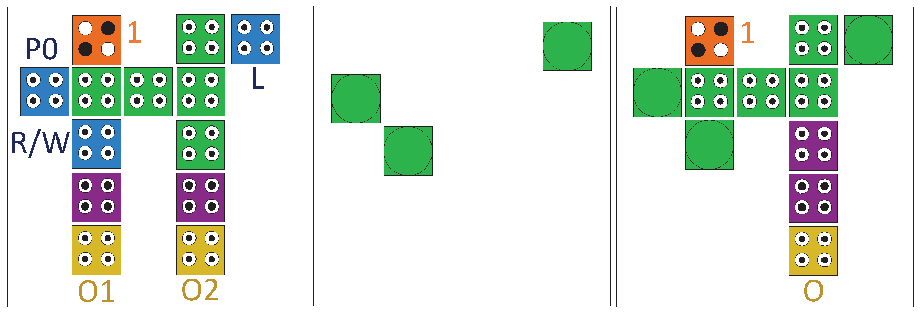
Figure 14.
Proposed reversible memory layers.
Figure 14.
Proposed reversible memory layers.
Figure 15.
Comparison between of the proposed block and previous works. a) Cost b) Number of cells.
Figure 15.
Comparison between of the proposed block and previous works. a) Cost b) Number of cells.
Figure 16.
a) Evaluation of the avg_ebath energy consumed, b) sum_ebath energy consumed by the proposed block and the previous works.
Figure 16.
a) Evaluation of the avg_ebath energy consumed, b) sum_ebath energy consumed by the proposed block and the previous works.
Table 1.
Various Logic Functions for Different Input Combinations of GDI Cell [
1].
Table 1.
Various Logic Functions for Different Input Combinations of GDI Cell [
1].
| N |
P |
G |
D |
Functions |
| 0 |
B |
A |
A’B |
F1 |
| B |
1 |
A |
A’+B |
F2 |
| 1 |
B |
A |
A+B |
OR |
| B |
0 |
A |
A.B |
AND |
| C |
B |
A |
A’B+AC |
Mux |
| 0 |
1 |
A |
A’ |
NOT |
Table 4.
This is a table. Tables should be placed in the main text near to the first time they are cited.
Table 4.
This is a table. Tables should be placed in the main text near to the first time they are cited.
| |
Tunneling Energy |
| |
0.5 EK |
1 EK |
1.5 EK |
| Avg Leakage Energy Dissipation |
0.0015 |
0.00459 |
0.00826 |
| Avg Switching Energy Dissipation |
0.00951 |
0.00835 |
0.00722 |
| Avg Energy Dissipation of circuit |
0.01101 |
0.01294 |
0.01549 |
| Max Kink Energy |
0.00148 |
0.00148 |
0.00148 |
Table 5.
Assessing the suggested MGDI cell in comparison to other existing works.
Table 5.
Assessing the suggested MGDI cell in comparison to other existing works.
| Reference |
Technique |
QCA cell count |
Area
𝛍m2) |
Latency
(Clock zones) |
Crossover type |
Cost
(Area*Latency) |
| [1] |
GDI |
16 |
0.02 |
2 |
Without |
0.022 |
| [21] |
ULG |
11 |
0.01 |
1 |
Coplanar |
0.01 |
| [22] |
ULG |
30 |
0.011 |
1 |
Without |
0.011 |
| [23] |
GDI |
19 |
0.02 |
1 |
Without |
0.02 |
| [25] |
GDI |
11 |
0.01 |
1 |
Without |
0.01 |
| Proposed |
MGDI |
9 |
0.01 |
1 |
Without |
0.01 |
Table 6.
Results of evaluation of energy lost in the proposed MGDI-QCA cell and previous works.
Table 6.
Results of evaluation of energy lost in the proposed MGDI-QCA cell and previous works.
| Reference |
Energy dissipation
(total) eV |
Energy dissipation
(average per cycle) eV |
| |
Sum_Ebath |
Error |
Avg_Ebath |
Error |
| [1] |
1.61e-002 |
-1.75e-003 |
1.47e-003 |
-1.59e-004 |
| [25] |
1.49e-002 |
-1.61e-003 |
1.35e-003 |
-1.46e-004 |
| Proposed |
0.845e-002 |
-0.907e-003 |
0.769e-003 |
-0.825e-004 |
Table 7.
Comparison results of MUX 2 * 1 in the proposed design with previous works.
Table 7.
Comparison results of MUX 2 * 1 in the proposed design with previous works.
| Reference |
QCA cell count |
Area
μm2) |
Latency
(Clock zones) |
Cost
(Area*Latency) |
| [34] |
15 |
0.01 |
2 |
0.02 |
| [35] |
12 |
0.01 |
1 |
0.01 |
| [36] |
16 |
0.02 |
2 |
0.04 |
| [23] |
19 |
0.02 |
3 |
0.06 |
| [1] |
39 |
0.126 |
2 |
0.252 |
| [25] |
11 |
0.01 |
1 |
0.01 |
| Proposed |
9 |
0.01 |
1 |
0.01 |
Table 8.
Comparative Results of XOR gate.
Table 8.
Comparative Results of XOR gate.
| Reference |
QCA cell count |
Area
μm2) |
Latency
(Clock zones) |
Cost
(Area*Latency) |
| [37] |
24 |
0.02 |
3 |
0.06 |
| [38] |
27 |
0.02 |
3 |
0.06 |
| [39] |
13 |
0.01 |
1 |
0.01 |
| Proposed |
9 |
0.01 |
1 |
0.01 |
Table 9.
Comparison result of single bit comparator.
Table 9.
Comparison result of single bit comparator.
| Reference |
QCA cell count |
Area
μm2) |
Latency
(Clock zones) |
Cost
(Area*Latency) |
| [40] |
85 |
0.06 |
5 |
0.3 |
| [41] |
58 |
0.05 |
3 |
0.15 |
| [42] |
42 |
0.05 |
3 |
0.15 |
| [29] |
38 |
0.03 |
2 |
0.06 |
| [12] |
37 |
0.06 |
3 |
0.18 |
| [43] |
35 |
0.04 |
3 |
0.12 |
| Proposed |
33 |
0.04 |
3 |
0.12 |
Table 10.
4-bit parity generator comparison results.
Table 10.
4-bit parity generator comparison results.
| Reference |
QCA cell count |
Area
μm2) |
Latency
(Clock zones) |
Cost
(Area*Latency) |
| [44] |
111 |
0.14 |
8 |
1.12 |
| [45] |
97 |
0.1 |
7 |
0.70 |
| [46] |
86 |
0.1 |
6 |
0.60 |
| [47] |
37 |
0.05 |
6 |
0.30 |
| [30] |
38 |
0.02 |
3 |
0.06 |
| Proposed |
29 |
0.06 |
3 |
0.18 |
Table 11.
D Flip-Flop comparison results.
Table 11.
D Flip-Flop comparison results.
| Reference |
QCA cell count |
Area
μm2) |
Latency
(Clock zones) |
Cost
(Area*Latency) |
| [48] |
37 |
0.03 |
6 |
0.18 |
| [28] |
21 |
0.02 |
5 |
0.1 |
| [49] |
24 |
0.02 |
5 |
0.1 |
| [50] |
23 |
0.02 |
4 |
0.08 |
| [51] |
19 |
0.02 |
3 |
0.06 |
| [31] |
13 |
0.01 |
3 |
0.03 |
| Proposed |
13 |
0.01 |
1 |
0.01 |
Table 12.
RAM comparison results.
Table 12.
RAM comparison results.
| Reference |
QCA cell count |
Area
μm2) |
Latency
(Clock zones) |
Cost
(Area*Latency) |
| [52] |
55 |
0.06 |
10 |
0.6 |
| [51] |
87 |
0.07 |
6 |
0.42 |
| [32] |
32 |
0.02 |
2 |
0.04 |
| [33] |
26 |
0.03 |
4 |
0.12 |
| Proposed |
27 |
0.02 |
2 |
0.04 |
