
Submitted:
21 November 2023
Posted:
21 November 2023
You are already at the latest version
Abstract
Porous structures and micropatterning surfaces play a crucial role in the development of highly sensitive force sensors. However, achieving these two conductive architectures typically requires complex materials synthesis and expensive manufacturing processes. In this study, we introduce a novel conductive composite film featuring a porous/micropyramid hybrid conductive architecture, which is achieved through a straightforward process of materials mixing and one-step screen printing. By utilizing a deep eutectic solvent in the ink component, micropores are induced in the printed composite, while the mesh of the screen mask acts as a template, resulting in a micropyramid film surface. We have successfully realized highly sensitive flexible force sensors with multifunctional capabilities for perceiving normal force and shear force.
Keywords:
printed flexible sensors
; conductive composite
; porous structure
; micropyramide structure
; multifunctional force detection.
1. Introduction
Flexible sensors have emerged as a promising technology in the domains of wearable technology and robotics, offering diverse applications including human-machine interfaces, prosthetics, and robotic manipulation. [1,2,3,4] Among the various categories of flexible sensors, flexible force sensors have garnered significant attention due to their capacity to accurately detect and quantify applied forces, thereby providing real-time force feedback to enhance user experience and safety. [5,6,7] Conductive composite materials have displayed remarkable potential in the development of flexible pressure sensors, owing to their excellent electrical conductivity and mechanical flexibility. [8,9] These materials facilitate seamless integration into flexible sensor designs, enabling them to conform to irregular surfaces, withstand deformations, and deliver reliable and precise force measurements. [10,11,12]
The sensitivity of pressure sensors is profoundly influenced by the morphology of the conductive film. [13,14] Two critical architectural features, microporous and micropatterned structures, play a pivotal role in enhancing pressure sensor sensitivity. [15,16,17,18,19,20,21,22,23,24,25] Microporous conductive structures induce a substantial change in bulk resistance when subjected to pressure, owing to their porous nature, which allows the elastic film to be easily compressed. Consequently, this results in heightened sensitivity and an extended sensing range. [15,16,17,18,19,20,21] Conversely, micropatterned structures are related to changes in contact resistance between the sensing layer and the electrode. The microstructure of the sensor mitigates abrupt on-off behavior due to gradually changing contact points, leading to an expanded working range. [22,23,24,25] However, the achievement of these desired microporous and micropatterned structures in conductive films presents significant challenges. Porous structures are typically realized through methods such as immersing porous materials like sponges in a conductive solution or employing a soluble template, such as sugar or salt, in a conductive polymer composite.[19,20] These techniques involve complex and time-consuming processes and present challenges for device patterning, often resulting in films with thicknesses in the order of several millimeters. Micropatterned surfaces are typically achieved through molding, which requires expensive templates. [23,24] More recently, natural-based patterning and laser abrasion have been explored, but they still necessitate multiple steps and often produce films of large dimensions that cannot be readily patterned on the target substrate. [26,27] These material and process limitations significantly hinder the practical application of these sensing structures.
This study introduces an innovative approach for fabricating a conductive film with a hybrid microporous/micropyramid architecture for flexible force sensors. This exceptional conductive architecture is achieved through the design of a composite ink and the selection of a fabrication method. We utilized a Deep Eutectic Solvent (DES) as a liquid template in a mixture of PDMS and graphite composite, which enabled the creation of a porous structure through an annealing process. By adjusting the ink's viscosity with a high graphite loading, we employed the screen-printing method with a mesh mask as the template during printing, resulting in a readily achievable micropyramid structure in the printed film. This proposed method offers advantages in terms of scalability, performance, and cost-effectiveness. We successfully realized high-performance pressure sensors and sensor arrays, demonstrating comprehensive capabilities in detecting pulse waves, human finger tapping, and shear forces.
2. Materials and Methods
2.1. Materials.
Poly(ethylene-phthalate) (PEN) film (Q65HA, 100-μm thick) was procured from Dupont. PDMS (Sylgard 184) was sourced from Dow Corning. Benzophenone (BP) and Diphenylamine (DP) were obtained from TCI Chemical. Graphite (20-micron powder) was purchased from Aldrich. Screen-printable Ag paste (XA-3797) was acquired from Fujikura Kasei, and the screen masks and stencil masks were obtained from SONOCOM CO., LTD. All materials were utilized as received.
2.2. Ink Synthesis.
The preparation of the printable composite inks was conducted in accordance with our prior publications [28,29,30], with minor adjustments. As depicted in Figure S1, BP and DP were blended in a 1:1 molar ratio to create a deep eutectic liquid. The resulting solid mixture was stored at room temperature for 2 hours or annealed at 90 °C for 30 minutes to yield a clear yellowish liquid. A suitable quantity of graphite powder was introduced to the deep eutectic solvent (DES) and blended using a planetary centrifugal mixer (THINKY MIXER AR-100) for 7 minutes (5 minutes of mixing and 2 minutes of degassing). The obtained DES-Graphite gel was further mixed with PDMS (base polymer: cure agent 10:1) using the mixer for 15 minutes to produce a slurry-like composite ink. In this investigation, the weight ratio of PDMS to DES was maintained at 1:1 in the final ink formulations. Detailed information on the ink formulations is provided in Table S1.
2.3. Sensor Fabrication.
The sensors were fabricated using an automatic screen printer (Micro-tec Co., Ltd.). Initially, electrodes were printed onto the PEN film using silver paste and then sintered at 150 °C for 30 minutes. Subsequently, the composite ink was printed on another PEN substrate, and an annealing process was conducted at 75 °C for 1 hour followed by 140 °C for 30 minutes to create the sensing layer. The sensing layer was cut into a circular shape using a knife and assembled to the electrodes in a face-to-face configuration. To ensure stability, a 3M telegram tape was employed to seal the device. The fabricated sensor was trimmed to the desired dimensions and affixed with an FPC connector for subsequent characterization and measurements.
2.4. Characterization.
An optical microscope (Keyence VHX-7000) was utilized to capture optical images of the printed traces and substrate. Scanning electron microscopy (SEM) images were obtained using a HITACHI tabletop microscope (TM4000Plus). Photographs and video of the sensors in the application demonstration were captured with a smartphone camera. The pressure-sensing tests were performed by a force gauge with an auto stage (IMADA). Resistance measurements were recorded using a digital multimeter (KEITHLEY DMM6500) with a 2-wire measurement setup. For the demonstration of human pulse wave and finger tape monitoring, the developed sensors were affixed to the hand of a male volunteer (34 years old).
3. Results and Discussion
3.1. Sensor design and fabrication
Constructing a porous structure or a micropatterned surface for a conductive film is widely acknowledged as two effective approaches to achieve high-performance resistive-type pressure sensors. However, methods for realizing such conductive structures, let alone a hybrid structure combining both architectures, have posed significant challenges. Researchers have intensively explored the use of sugar templates (or salt particles) to create porous structures, often without highlighting the difficulties associated with template removal, thin film formation, and patterning. Meanwhile, micropatterning surfaces typically involve multi-step molding processes with high costs, making them less conducive to scalable manufacturing. While these conventional methods may hold academic value, they fall short in promoting the practical application of flexible sensors, creating a gap between sensor performance and manufacturability. Differing from these previous methods, we have developed a one-step process that involves selecting the right material system and adjusting viscosity while utilizing a printing mask. The sensor layer is realized through a single-step screen printing and annealing process, as depicted in Figure 1a. This scalable approach, devoid of complex treatments, allows for the straightforward production of devices suitable for both mass production and well-defined patterning (see Figure S2). The printed sensing layer and the printed electrode layer are seamlessly assembled face-to-face and sealed using a 3M tape, enabling us to easily create devices with both single sensor patterns and sensor arrays (Figure 1b).
The formation of the hybrid porous/pyramid structure can be attributed to the design of the material system and the selection of the printing process (Figure 1c). The ink is based on our previous discovery, wherein a deep eutectic solvent (DES) induces phase separation between carbon materials and PDMS, serving as a liquid template for the formation of a porous structure.[28] This ink system enables the realization of a porous structure with a one-step printing and annealing process. We use graphite as the conductive filler for this ink and have discovered that it can form a multiscale porous structure due to the porous nature of the graphite powder. As for the micropyramid surface morphology, we have innovatively designed a new approach that using the screen mask to induce it. The screen mask includes microscale mesh, and by adjusting the ink viscosity, the micropyramid structures are raised by the screen mesh during the lift-off of the screen printing mask. This ingenious design allows for the in-situ formation of the micropyramid structure.
The expected working mechanism of the printed sensors is illustrated in Figure 1d, where the hybrid conductive structure induces a hybrid response mode. When pressure is applied to the sensor, the film's pores are compressed, resulting in an increase in the conductive pathways for the graphite and, consequently, a decrease in resistance. Simultaneously, the contact points between the sensing layer and electrode layer increase due to the micropatterned structure, also leading to a decrease in resistance. The combined effect is expected to result in a high-performance sensor compared to those with only individual structures. Thus, in this work, we have developed a sensor that combines the advantages of both conductive structures but achieves this using a significantly simpler process than each of them individually. We believe that this design will have a profound impact on sensor development, benefiting both academia and industry alike.
3.2. Morphology control of printed sensing layers
The scanning electron microscopy (SEM) images of the surface morphologies of the printed film are depicted in Figure 2. Within the developed ink formulations, the weight ratio of PDMS to DES was consistently maintained at 1:1. However, the graphite loading was varied, with values of 0.5, 0.75, 1, and 1.25 for ink-1, ink-2, ink-3, and ink-4, respectively. As illustrated in Figure 2a-2e, it is evident that as the graphite loading increases, the surface morphology becomes progressively more distinct. At lower loadings, the surface retains a smooth appearance, primarily due to the leveling effect of the printed ink. In contrast, ink-4 exhibits a well-defined micropyramid structure with a height of 50 micrometers. The pitch size of 250 micrometers perfectly matches the dimensions of the screen mesh (Figure S3), suggesting that the micropyramid is generated through the lift-off process of the screen mask and maintained after annealing, owing to the high viscosity induced by the elevated graphite loading. Further increases in graphite loading make the printing process more challenging, resulting in a grid-like texture on the film's surface, akin to imprinting, with less uniformity (Figure S4). Consequently, ink-4 is defined as the optimal ink formulation.
In Figure 2e, a cross-section image of the printed film reveals a multiscale porous structure. The larger pores are consistent with our prior findings, attributed to the phase separation between PDMS and graphite induced by DES. Meanwhile, the smaller pores are a consequence of the loose packing of graphite powder after DES evaporation. As a result, we successfully achieved a hybrid microporous/micropyramid structure through a one-step printing process. To validate the template effect of the screen mesh mask, we also printed the film using ink-4 with a stencil mask that lacks a mesh structure. As shown in Figure 2f and 2g, the composite film produced via stencil printing exhibits a relatively smooth surface, though phase separation and porous structures are still evident (Figure 2g). These results unequivocally confirm the formation mechanism described in Figure 1c. The porous structure is induced by the DES, while the screen mesh induces a micropyramid structure. Thus, we have achieved a complex conductive architecture through a one-step printing and annealing process, facilitated by the ingenious design of the ink and the selection of the fabrication process.
3.3. Characterization of sensing performance
The electrical-mechanical performance of the printed sensors has been thoroughly characterized and is presented in Figure 3. The presence of the micropyramid structure plays a pivotal role in enhancing the sensor's sensing range while maintaining a high level of sensitivity. It is a well-known challenge that sensors relying on contact resistance often suffer from a limited sensing range, resulting in an on-off behavior. As depicted in Figure 3a, the composite films based on ink-1 and ink-2 exhibit this on-off behavior due to their smooth surface morphologies. In contrast, the sensor based on ink-4 demonstrates excellent pressure sensing performance with both remarkable sensitivity and an extended sensing range. It's important to note that ink-1 and ink-2 appear to have higher sensitivity than ink-4. However, this is primarily attributed to their initially higher resistance and a substantial resistance change within a limited sensing range. Initial resistance is a crucial factor to consider in contact resistance-based sensors. An uncontacted state may yield high sensitivity values, but it is not suitable for accurately measuring pressure. The introduction of micropyramid structure enhanced the sensing ability of the sensor at the small pressure region.
We also compared the pressure sensing performance of sensors based on different printing methods, as illustrated in Figure 3b. Screen-printed films display superior sensing performance, while stencil-printed films exhibit an on-off behavior due to the absence of the micropatterned surface structure. For sensors without a porous structure, we conducted a performance characterization, as shown in Figure S5. These sensors exhibited pressure responses within a small sensing range. However, upon further force increase, a positive piezoelectric effect was observed. This behavior is attributed to the interaction between the PDMS and graphite within a randomly structured composite, consistent with the results reported in our prior work. [28,29] Hence, the combination of a porous structure and the pyramid structure significantly contributes to the reliability, sensitivity, and expanded sensing range of the sensor. For further characterization, we selected the screen-printed sensor using ink-4 as the optimized sensor. This sensor displayed a rapid response when subjected to a transient force of 0.5N, with a response time calculated at 116ms and a recovery time of 178ms (Figure 3c). Cyclic stability is another critical parameter for sensors. As shown in Figure 3d and Figure 3e, we subjected the sensor to a cyclic force of 1.5N for 1000 cycles, and the resistance changes remained consistently stable without significant degradation. These rapid responses and excellent stability undoubtedly underscore the sensor's potential for real-world applications.
3.4. Application Demonstrations
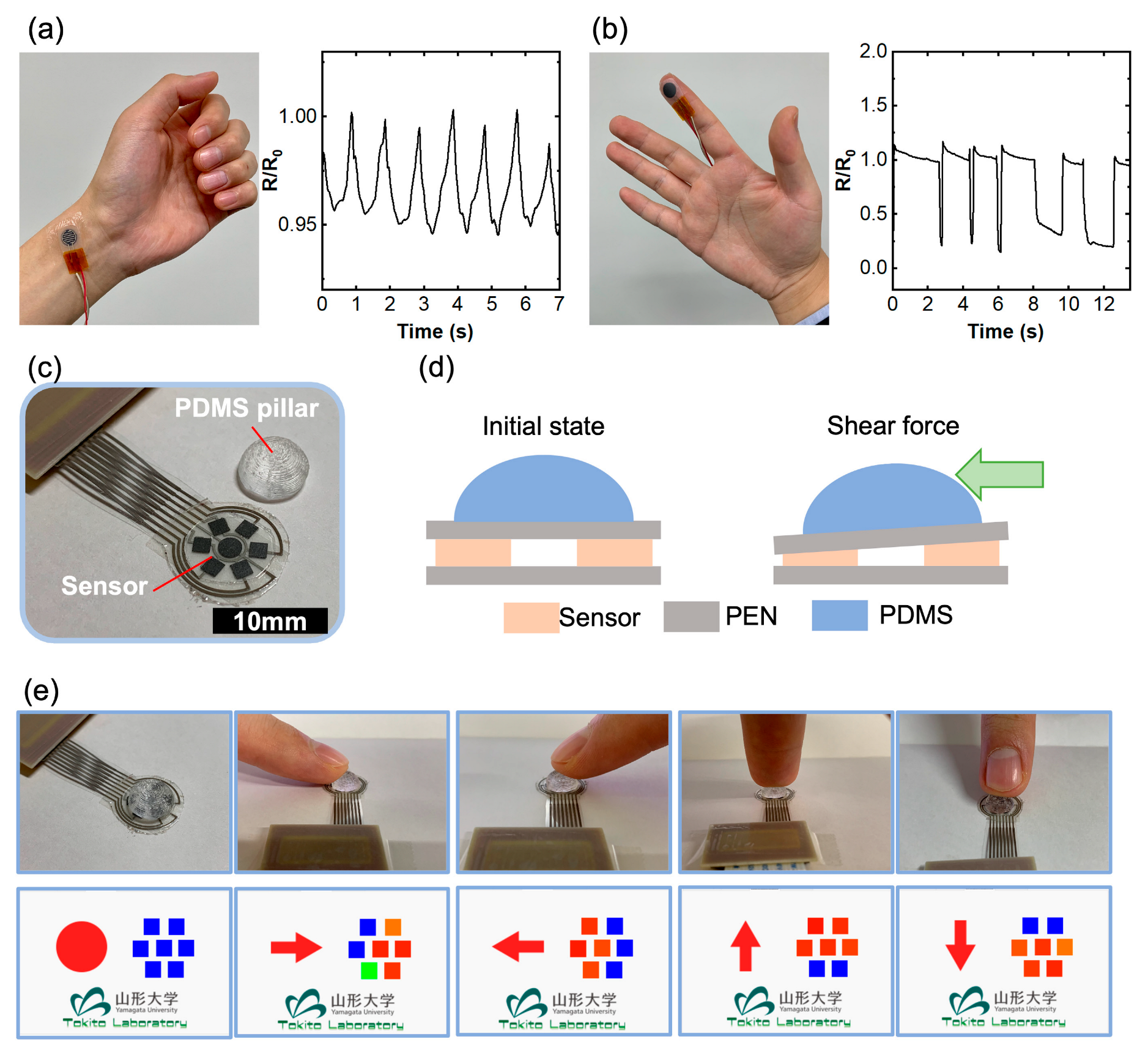
As previously described, the sensor's ease of fabrication, scalability, and patterning, combined with its high-performance electrical-mechanical detection capabilities, make it a versatile tool with the potential for various applications. Figure 4 presents a proof-of-concept demonstration of our developed sensor. When attached to the human wrist, the sensor exhibits a pronounced resistance change that correlates with the pulse wave, as illustrated in Figure 4a. This response is attributed to the high sensitivity, fast response time, and flexibility of our sensor. It underscores the sensor's potential for development as a high-performance healthcare device. Additionally, our sensor finds utility in monitoring human hand gestures when affixed to the fingertip, as demonstrated in Figure 4b. The distinct resistance changes observed during different finger tapping provide evidence of the sensor's applicability for human motion monitoring devices, including applications in augmented reality (AR) and virtual reality (VR).
The sensor's exceptional patterning capability allows for the creation of high-resolution sensor arrays, with individual sensor units as small as 2mm by 2mm. To illustrate this, we designed a 7-sensor array with one sensor in the center and six surrounding sensors for shear force detection. A PDMS pillar is employed to redistribute applied shear force as normal force (Figure 4c). The sensing mechanism is elucidated in Figure 4d: when a shear force is applied to the PDMS pillar from one side, an asymmetric normal force is generated due to the PDMS pillar, with one side experiencing a lesser force and the other side encountering a greater force. Consequently, the force direction can be easily detected. With six sensors in this array, the system demonstrates a resolution of 30 degrees. By integrating an Arduino and GUI design, we successfully showcase shear force detection, as depicted in Figure 4e and Supporting Video S1. With the further development of software and algorithms, the magnitude of force can also be accurately evaluated. These results clearly validate the advantages of our printed sensors in practical applications as multifunctional force sensors, opening up opportunities for a wide range of applications.
4. Conclusions
In this study, we have introduced a straightforward and innovative approach for the fabrication of a novel conductive composite film, characterized by a hybrid microporous/micropyramid structure. This development has enabled the creation of high-performance flexible pressure sensors designed to address multifunctional force perception requirements. The construction of complex conductive architectures, such as the combination of microporous and micropatterning structures, has posed a significant challenge in the field of flexible sensors. As a result, a disparity has existed between high-performance sensor capabilities and practical manufacturing processes. In this work, we have pioneered the use of a porous ink in conjunction with screen mesh printing to achieve a hybrid microporous/micropyramid structure through a straightforward, single-step printing and annealing process. This innovative approach eliminates the need for complex and costly procedures that previous research endeavors have often required. Our research provides a fresh perspective on overcoming the challenges associated with high-performance conductive composites, leveraging skillful ink design and process selection. Its significance extends to both academic exploration and industrial utilization, bridging the gap between sensor capabilities and real-world manufacturing processes.
Supplementary Materials
The following supporting information can be downloaded at the website of this paper posted on Preprints.org, Figure S1: The synthesis process of the printed composite ink; Table S1: Component of the printable composite inks; Figure S2: A printed sensing layer with pattern feature of 2 mm by 2 mm; Figure S3: Optical microscopy image of the screen mesh mask; Figure S4: SEM images of Ink-5 with high loading of Graphite; Figure S5: Comparison of performance of inks with DES (ink-4) and without DES (ink-0).Video S1: Demonstration of shear force detection by a printed sensor array.
Author Contributions
Conceptualization, Y.-F.W.; investigation, Y.-F.W., J.Y., and A.Y.; methodology, Y.-F.W., J.Y. T. K., and T.S.; resources, Y.-F.W., Y.T., T.S., D.K. and S.T.; supervision, S.T.; validation, Y.-F.W.; visualization, Y.-F.W. and J.Y.; writing—original draft, Y.-F.W., J.Y. and D.K.; writing—review and editing, Y.-F.W., T.S. and S.T. All authors have read and agreed to the published version of the manuscript.
Funding
This work was partially supported by JSPS KAKENHI Grant Number 23K13806.
Institutional Review Board Statement
The experiments involving the monitoring of human pulse waves and finger tapping were conducted with the approval of the Yamagata University's institutional review board (R05-16).
Data Availability Statement
Data sharing is not applicable to this article.
Acknowledgments
The authors thank Ms. Minako Watanabe for her indispensable support and assistance throughout the research process.
Conflicts of Interest
The authors declare no conflict of interest.
References
- Wang, M., Luo, Y., Wang, T., Wan, C., Pan, L., Pan, S., ... & Chen, X. Artificial skin perception. Advanced Materials, 2021, 33, 2003014. [Google Scholar] [CrossRef]
- Shih, B.; Shah, D.; Li, J.; Thuruthel, T.; Park, Y.; Iida, F.; Bao, Z.; Kramer-Bottiglio, R.; Tolley, M. Electronic Skins and Machine Learning for Intelligent Soft Robots. Science Robotics 2020, 5, eaaz9239. [Google Scholar] [CrossRef] [PubMed]
- Pang, G., Yang, G., & Pang, Z. Review of robot skin: A potential enabler for safe collaboration, immersive teleoperation, and affective interaction of future collaborative robots. IEEE Transactions on Medical Robotics and Bionics 2021, 3, 681–700. [Google Scholar] [CrossRef]
- Heng, W., Samuel, S., and Wei, Gao. Flexible electronics and devices as human–machine interfaces for medical robotics. Advanced Materials 2022, 34, 2107902. [Google Scholar] [CrossRef] [PubMed]
- Amjadi, M.; Kyung, K. U.; Park, I.; Sitti, M. Stretchable, skin-mountable, and wearable strain sensors and their potential applications: a review. Adv. Funct. Mater. 2016, 26, 1678. [Google Scholar] [CrossRef]
- Trung, T. Q.; Lee, N. E. Flexible and stretchable physical sensor integrated platforms for wearable human-activity monitoring and personal healthcare. Adv. Mater. 2016, 28, 4338. [Google Scholar] [CrossRef] [PubMed]
- Zhao, S.; Li, J.; Cao, D.; Zhang, G.; Li, J.; Li, K.; Yang, Y.; Wang, W.; Jin, Y.; Sun, R.; Wong, C. Recent Advancements in Flexible and Stretchable Electrodes for Electromechanical Sensors: Strategies, Materials, And Features. ACS Applied Materials & Interfaces 2017, 9, 12147–12164. [Google Scholar]
- Liu, H.; Li, Q.; Zhang, S.; Yin, R.; Liu, X.; He, Y.; Dai, K.; Shan, C.; Guo, J.; Liu, C.; Shen, C.; Wang, X.; Wang, N.; Wang, Z.; Wei, R.; Guo, Z. Electrically Conductive Polymer Composites For Smart Flexible Strain Sensors: A Critical Review. Journal of Materials Chemistry C 2018, 6, 12121–12141. [Google Scholar] [CrossRef]
- Yao, S.; Swetha, P.; Zhu, Y. Nanomaterial-Enabled Wearable Sensors for Healthcare. Advanced Healthcare Materials 2017, 7, 1700889. [Google Scholar] [CrossRef]
- Hong, Y., Wang, B., Lin, W., Jin, L., Liu, S., Luo, X., ... & Yang, Z. Highly anisotropic and flexible piezoceramic kirigami for preventing joint disorders. Science advances 2021, 7, eabf0795. [Google Scholar] [CrossRef]
- Liu, H., Zhao, H., Li, S., Hu, J., Zheng, X., Li, R., ... & Su, Y. Adhesion-Free Thin-Film-Like Curvature Sensors Integrated on Flexible and Wearable Electronics for Monitoring Bending of Joints and Various Body Gestures. Advanced Materials Technologies 2019, 4, 1800327. [Google Scholar] [CrossRef]
- Ma, C.; Xu, D.; Huang, Y.C.; Wang, P.; Huang, J.; Zhou, J.; Liu, W.; Li, S.T.; Huang, Y.; Duan, X. Robust Flexible Pressure Sensors Made from Conductive Micropyramids for Manipulation Tasks. ACS Nano 2020, 14, 12866–12876. [Google Scholar] [CrossRef] [PubMed]
- Niu, H.; Zhang, H.; Yue, W.; Gao, S.; Kan, H.; Zhang, C.; Zhang, C.; Pang, J.; Lou, Z.; Wang, L.; et al. Micro-Nano Processing of Active Layers in Flexible Tactile Sensors via Template Methods: A Review. Small 2021, 17, 2100804. [Google Scholar] [CrossRef] [PubMed]
- Ruth, S.R.A.; Feig, V.R.; Tran, H.; Bao, Z. Microengineering Pressure Sensor Active Layers for Improved Performance. Adv. Funct. Mater. 2020, 30, 2003491. [Google Scholar] [CrossRef]
- Ding, Y.; Xu, T.; Onyilagha, O.; Fong, H.; Zhu, Z. Recent Advances in Flexible and Wearable Pressure Sensors Based on Piezoresistive 3D Monolithic Conductive Sponges. ACS Applied Materials & Interfaces 2019, 11, 6685–6704. [Google Scholar]
- Sun, Q.; Zhao, X.; Zhou, Y.; Yeung, C.; Wu, W.; Venkatesh, S.; Xu, Z.; Wylie, J.; Li, W.; Roy, V. Fingertip-Skin-Inspired Highly Sensitive and Multifunctional Sensor with Hierarchically Structured Conductive graphite/Polydimethylsiloxane Foams. Advanced Functional Materials 2019, 29, 1808829. [Google Scholar] [CrossRef]
- Zhou, C.; Sun, W.; Jia, L.; Xu, L.; Dai, K.; Yan, D.; Li, Z. Highly Stretchable and Sensitive Strain Sensor with Porous Segregated Conductive Network. ACS Applied Materials & Interfaces 2019, 11, 37094–37102. [Google Scholar]
- Guo, H.; Tan, Y.J.; Chen, G.; Wang, Z.; Susanto, G.J.; See, H.H.; Tee, B.C. Artificially innervated self-healing foams as synthetic piezo-impedance sensor skins. Nat. Commun. 2020, 11, 5747. [Google Scholar] [CrossRef] [PubMed]
- Tewari, A.; Gandla, S.; Bohm, S.; McNeill, C.R.; Gupta, D. Highly Exfoliated MWNT–rGO Ink-Wrapped Polyurethane Foam for Piezoresistive Pressure Sensor Applications. ACS Appl. Mater. Interfaces 2018, 10, 5185–5195. [Google Scholar] [CrossRef] [PubMed]
- Mu, C.; Song, Y.; Huang, W.; Ran, A.; Sun, R.; Xie, W.; Zhang, H. Flexible Normal-Tangential Force Sensor with Opposite Resistance Responding for Highly Sensitive Artificial Skin. Adv. Funct. Mater. 2018, 28, 1707503. [Google Scholar] [CrossRef]
- Zhao, X.; Wang, W.; Wang, Z.; Wang, J.; Huang, T.; Dong, J.; Zhang, Q. Flexible PEDOT:PSS/Polyimide Aerogels with Linearly Responsive and Stable Properties for Piezoresistive Sensor Applications. Chem. Eng. J. 2020, 395, 125115. [Google Scholar] [CrossRef]
- Pan, L.; Chortos, A.; Yu, G.; Wang, Y.; Isaacson, S.; Allen, R.; Shi, Y.; Dauskardt, R.; Bao, Z. An ultra-sensitive resistive pressure sensor based on hollow-sphere microstructure induced elasticity in conducting polymer film. Nat. Commun. 2014, 5, 3002–3010. [Google Scholar] [CrossRef] [PubMed]
- Peng, S.; Blanloeuil, P.; Wu, S.; Wang, C.H. Rational Design of Ultrasensitive Pressure Sensors by Tailoring Microscopic Features. Adv. Mater. Interfaces 2018, 5, 1800403. [Google Scholar] [CrossRef]
- Wu, C. A new approach for an ultrasensitive tactile sensor covering an ultrawide pressure range based on the hierarchical pressure-peak effect. Nanoscale Horiz. 2020, 5, 541–552. [Google Scholar] [CrossRef]
- Xu, Z.; Wu, D.; Chen, Z.; Wang, Z.; Cao, C.; Shao, X.; Zhou, G.; Zhang, S.; Wang, L.; Sun, D. A flexible pressure sensor with highly customizable sensitivity and linearity via positive design of microhierarchical structures with a hyperelastic model. Microsyst. Nanoeng. 2023, 9, 5. [Google Scholar] [CrossRef] [PubMed]
- Zhao, T.; Li, T.; Chen, L.; Yuan, L.; Li, X.; Zhang, J. Highly Sensitive Flexible Piezoresistive Pressure Sensor Developed Using Biomimetically Textured Porous Materials. ACS Appl. Mater. Interfaces 2019, 11, 29466–29473. [Google Scholar] [CrossRef] [PubMed]
- Guo, X.; Ma, L.; Wu, W.; Li, S.; Lei, X.; Wu, X.; Yu, X.; Liu, F. Ultra-sensitive flexible piezoresistive pressure sensor prepared by laser-assisted copper template for health monitoring. Sens. Actuators A Phys. 2022, 334, 113325. [Google Scholar] [CrossRef]
- Wang, Y. F., Sekine, T., Takeda, Y., Hong, J., Yoshida, A., Kumaki, D., ... & Tokito, S. Deep eutectic solvent induced porous conductive composite for fully printed piezoresistive pressure sensor. Advanced Materials Technologies 2021, 6, 2100731. [Google Scholar] [CrossRef]
- Yoshida, A., Wang, Y. F., Sekine, T., Takeda, Y., Kumaki, D., & Tokito, S. Printed Low-Hysteresis Stretchable Strain Sensor Based on a Self-Segregating Conductive Composite. ACS Applied Engineering Materials 2023, 1, 50–58. [Google Scholar] [CrossRef]
- Wang, F.; Yoshida, A.; Takeda, F.; Sekine, T.; Kumaki, D.; Tokito, S. Printed Directional Bending Sensor with High Sensitivity and Low Hysteresis for Human Motion Detection and Soft Robotic Perception. Sensors 2023, 23, 5041. [Google Scholar] [CrossRef]
Figure 1.
(a) Schematic of the fabrication process for the printed pressure sensor. (b) Illustration of the sensor structure showcasing the hybrid porous/micropyramid conductive architecture and a photograph of the printed sensors. (c) Illustrating the formation mechanism of the sensing layer with the hybrid porous/micropyramid conductive architecture. (d) Diagram illustrating the pressure sensing mechanism of the printed sensors.
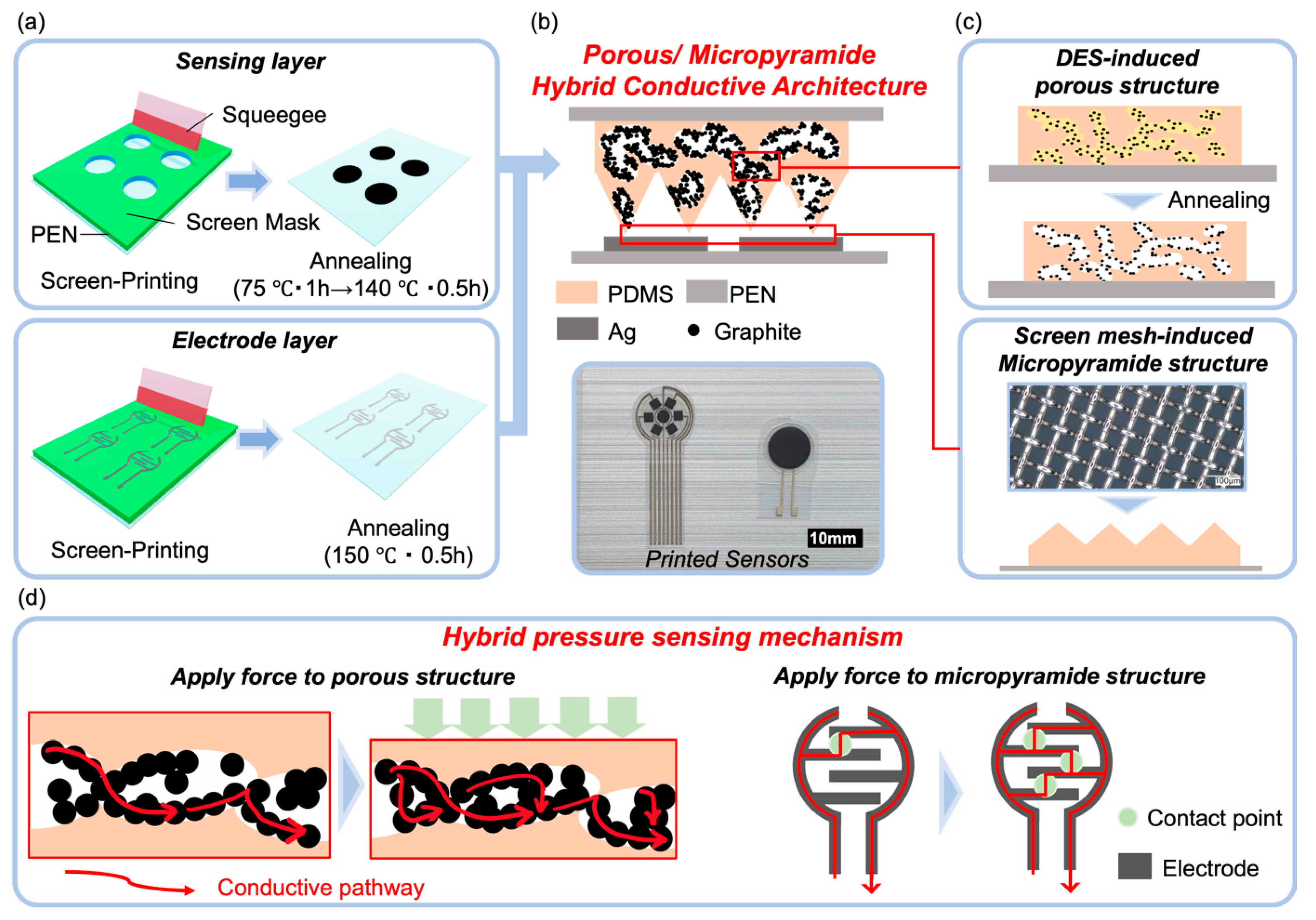
Figure 2.
Surface Morphologies of the Printed Composite Films. (a-c) SEM images taken at a 45-degree observation angle of the screen-printed conductive films using (a) ink-1, (b) ink-2, (c) ink-3, and (d) ink-4. (e) Cross-sectional SEM image of the screen-printed conductive film using ink-4, highlighting the typical large pores marked by a yellow curve and small pores marked by a red curve. (f) SEM image at a 45-degree observation angle of the stencil-printed conductive films using ink-4. (g) Cross-sectional SEM image of the stencil-printed conductive film using ink-4. Scale bars: (a-d, f) 500 μm; (e, g) 100 μm.
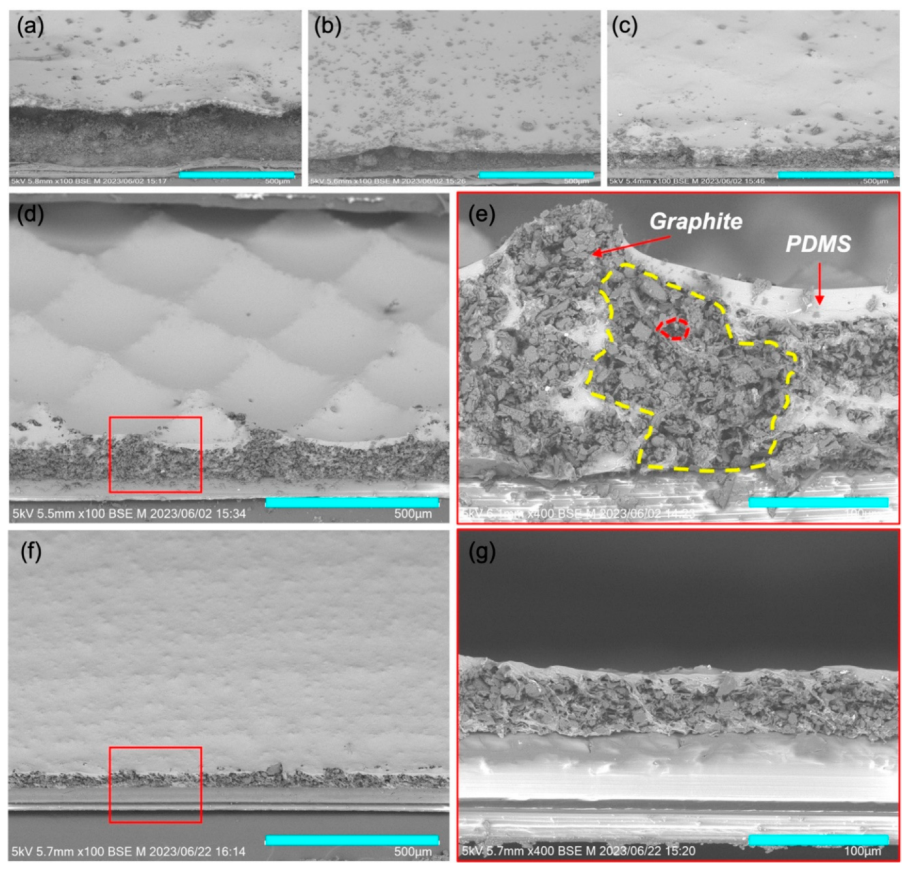
Figure 3.
Electrical-Mechanical Performances of Sensors with Various Composite Films. (a) Relative resistance changes in screen-printed sensors using composite films of ink-2, ink-3, and ink-4 under varying applied pressures. (b) Relative resistance changes in sensors utilizing the composite film of ink-4, comparing screen printing and stencil printing under different applied pressures. (c) Response and recovery times of a screen-printed sensor based on ink-4. (d) Stability assessment of a screen-printed sensor based on ink-4 under a cyclic force of 1.5N for 1000 cycles. (e) Enlarged image of the measurement results shown in the red frame of (d).
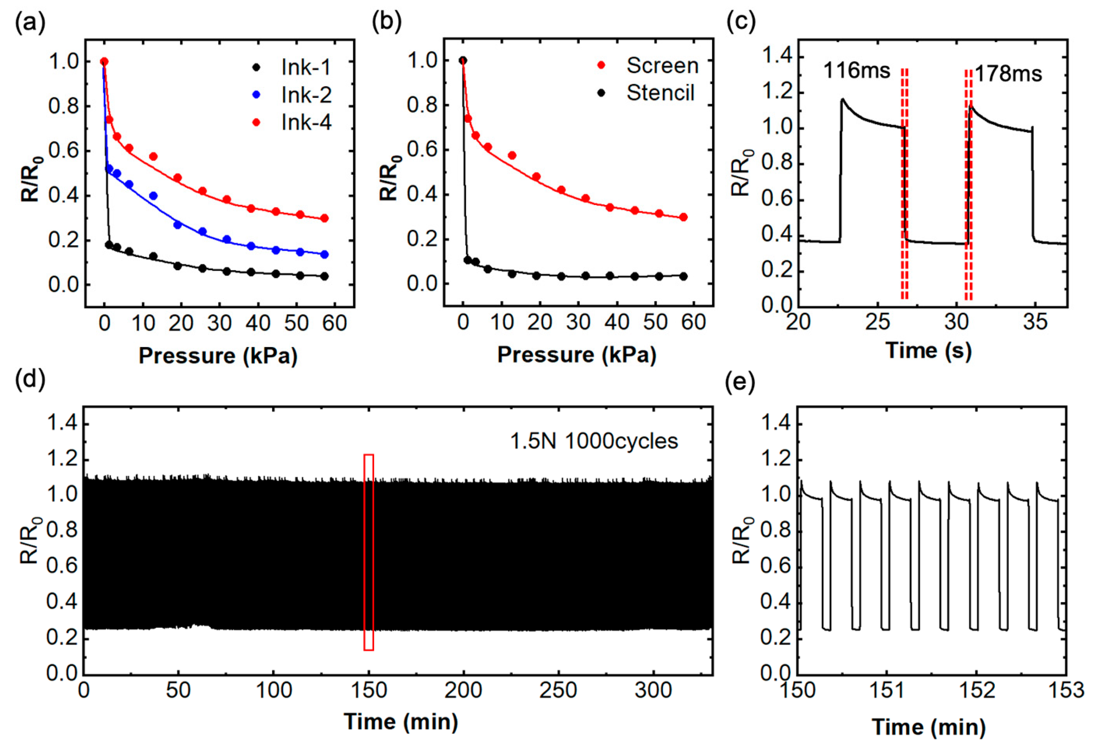
Figure 4.
Application Demonstrations of the Printed Sensors. (a) A single printed sensor affixed to the human wrist for the measurement of pulse waves. (b) A single printed sensor attached to the fingertip for monitoring finger tapping. (c) A printed sensor array designed for shear force detection. (d) Illustration of the mechanism behind shear force detection. (e) Results of shear force detection facilitated by a GUI system, demonstrating sensor response as the finger exerts pressure on the PDMS pillar from various directions.
Disclaimer/Publisher’s Note: The statements, opinions and data contained in all publications are solely those of the individual author(s) and contributor(s) and not of MDPI and/or the editor(s). MDPI and/or the editor(s) disclaim responsibility for any injury to people or property resulting from any ideas, methods, instructions or products referred to in the content. |
© 2023 by the authors. Licensee MDPI, Basel, Switzerland. This article is an open access article distributed under the terms and conditions of the Creative Commons Attribution (CC BY) license (http://creativecommons.org/licenses/by/4.0/).
Copyright: This open access article is published under a Creative Commons CC BY 4.0 license, which permit the free download, distribution, and reuse, provided that the author and preprint are cited in any reuse.


