Preprint
Article

Effect of Cracks at Shallow Depths during Nanoindentation in Titanium Diboride Hard Coatings

Altmetrics

Downloads

61

Views

18

Comments

0

This version is not peer-reviewed

Submitted:

24 November 2023

Posted:

27 November 2023

You are already at the latest version

Alerts
Abstract
Hard coatings like Titanium diboride (TiB2) on silicon substrates are used for interconnects. micro-electro-mechanical devices and metallurgical protective coatings were analyzed based on shallow depths of nanoindentation penetration which involves a change in the nature of the contact from Hertzian to Pyramidal both in loading as well as unloading modes. Features like ductile fracture, linear unloading, and the creation of electrical conduction paths were analyzed. These high-precision features are influenced by the thickness and crystalline nature of the films and are significant for device fabrication.
Keywords: 
Subject: Engineering  -   Metallurgy and Metallurgical Engineering

1. Introduction

Hard coatings of Titanium diboride (TiB2) are used for metallurgical protection as well as in the microelectronic industry as micro-electro-mechanical systems (MEMS) components or interconnects. The wear and abrasion properties of these coatings are therefore significant and require high-precision inspection. The nature of contact established between the indenter and the sample at shallow depths may reveal novel features related to elastic-plastic response and internal through-thickness (ductile) crack generation and propagation due to different complexions of stress imposed underneath the indenter. A change in contact takes place with increased depth of penetration. The crystalline nature of the sample also influences the indenter penetration and subsequent response [1,2]. An attempt has been made in this communication to address and analyze some of the shallow depth indentation features of hard coatings of TiB2.

2. Materials and Methods

Titanium diboride coatings were deposited on silicon substrates using RF magnetron sputtering (HINDHIVAC, Bangalore) using sintered ceramic target, the details which have been reported previously. Nanoindentation (MTS, USA) based on continuous stiffness mode (CSM) was performed on these coatings with an emphasis on lower depths of penetration [3]. Atomic Force Microscopy (SEIKO 400 Japan) was used in imaging the indenter penetration at higher loads.

3. Results and discussions

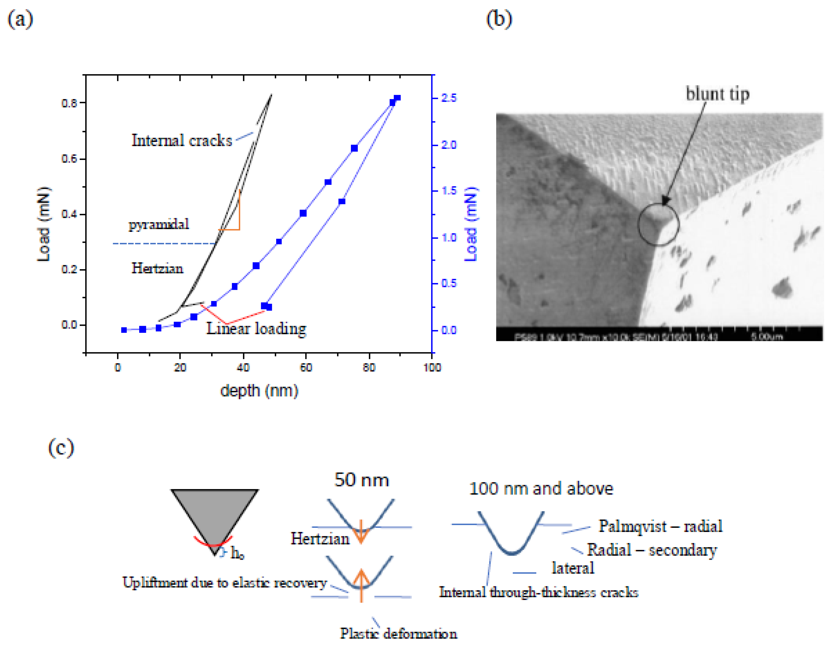
The load-depth (P-h) plot for indentations performed at 50 and 100 nm depths is shown in Figure 1(a). Interesting features of high elastic recovery and a discontinuity in the loading curve suggesting internal cracking were observed. A feeble plastic deformation is visible in the plot but there seems to be no residual depth. A ductile fracture can be inferred from these observations. Although a sharp three-sided pyramidal Berkovich indenter has been used, the contact established in such a shallow depth of 50 nm is Hertzian in nature mainly due to tip bluntness as depicted in the SEM image in Figure 1 (b) [4]. For deeper penetration of 100 nm, the usual nature of the P-h plot was found. A linear loading at the end of the unloading curve was observed in both cases where the indenter seems to be penetrating back into the sample without any application of load. The extent of linear unloading was higher for lower depths of penetration (50 nm). The contact is Hertzian till 28 nm (0.5 mN) and offers negligible plastic deformation. A deeper penetration changes the contact from Hertzian to pyramidal. The sharper contact provides high stress to any flaws pre-existing causing an internal fracture which gets expressed as a discontinuity (pop-in) in the plot. Pop-in events depict phononic friction induced in nanoindentation. An enhancement in lattice friction causes increased resistance to dislocation motion and as a result smaller pop-in width [5]. Heterogeneous nucleation usually results in in-distinctive pop-ins [6]. The energy stored before pop-in gets utilized in the plastic deformation during pop-in [7].
A plastic deformation seems to be taking place as observed from the unloading plot till the contact again becomes Hertzian at 28 nm. A unique phenomenon of indentation impression being existent underneath the top surface but is not observable from the top. It indicates a very important observation that when subjected to shallow depths, the sample might not show deformation from the top surface but might have gone deformation or damage underneath. Being no indentation impression being formed at the top, the material recovers elastically. The release stress-induced however gets released by means of upliftment of the film surface from its pre-indented state establishing contact with the indenter resulting in linear unloading (Figure 1 c). This phenomenon although occurring for 100 nm penetration as well, the intensity is much less. The internal cracks were also not so much prevailing for 100 nm penetration. This is because the tip sharpness is related to the ratio of compressive stress and shear stress being imposed. A sharper tip imposes a higher fraction of compressive stress than shear stress causing plastic deformation. For ductile failure, as the film thickness increases, the fracture toughness also increases but is followed by a decrease due to the transition from plane stress to plain strain condition, until a plateau is reached, after which the toughness remains insensitive to further increase in thickness.
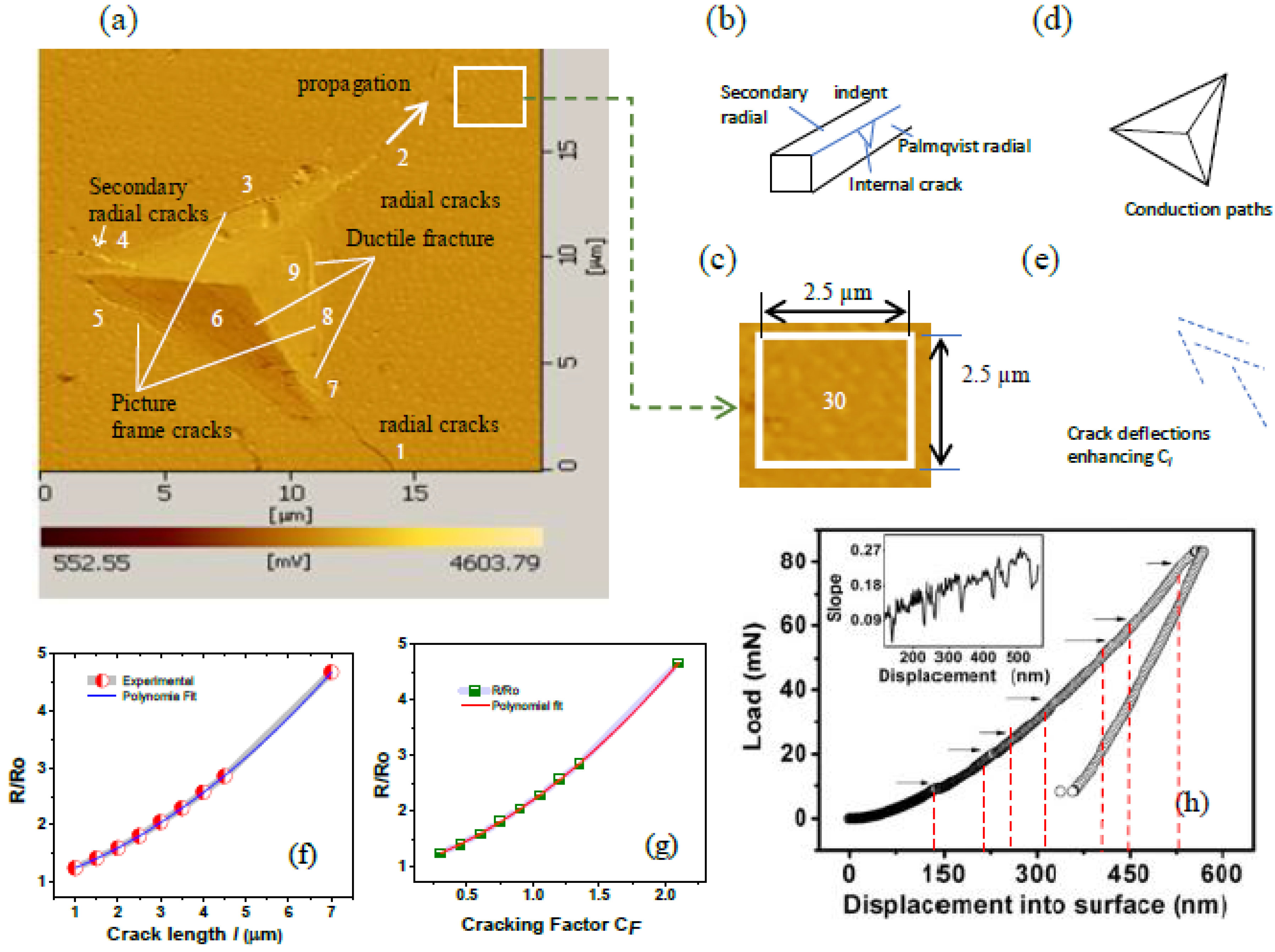
The zero-point correction due to tip blunting makes the contact depth hc represented as hc = α (h – P/S + ho) where ho is the equivalent height of the tip defect as shown in Figure 1(c), taken as 5 nm approximately. S is the stiffness (0.02 mN/nm) and α = 1.2 for the Berkovich indenter which is due to pile-up or sink-in [8]. Due to tip blunting, the initial contact of the indenter tip for shallow depth (50 nm) with the sample is Hertzian (as for a spherical indenter). For higher indentation depths, sides of the indenter come in contact and the Hertzian contact is no more prevalent. The increased sharpness causes crack growth as shown in the schema. Palmqvist radial and secondary radial cracks are shown cross-sectionally in Figure 1 (c), evidence of which can be found below (Figure 2a). Palmqvist-radial, secondary-radial, picture frame, and through-thickness cracks can be observed originating from different regions of the nanoindentation impression whose cross-sectional schematic representation The dotted line showing indentation contact edges deviated from a geometrically perfect shape. These cracks are related to the toughness and adhesion of the films. The mechanism of different crack generation in nanoindentation can be found in ref [9]. The formation of high-density of nanocrystallites (4.8 µm-2) in the sputter deposition process provided resistance to crack propagation causing deflections indicating enhanced toughness (Figure 2 c).
Internal through-thickness cracks occur and are arrested in the indenter impression region. They are evidence of ductile to brittle transitions. In ductile fracture, appreciable plastic deformation occurs before crack initiation and during crack propagation. As observed above, the Berkovich indenter is specially made to cause plastic deformation even at shallow depths, DBT again results in. cracks which are internal (inside the and have not been able to propagate to the surface. Based upon the mV scale bar, the conduction paths in the indent and originating through the cracks, as well as crystallites, can be identified (Figure 2 d) which are significant for the TiB2 films used in interconnects.
The distribution of cracks particularly the crack density and size in a solid influence the conduction properties of a material [10]. Evidence of conductive bridges within the cracks has been found [11,12]. A parameter known as cracking factor CF defined as the product of crack length (a) and linear crack density (Cl, no. of cracks per unit length) can be used in relation to the conductivity (relative resistance) of films as given in eqn 1 [13] where Ro is the resistance without any cracking. The indentation sides are 10 µm in length and associated with radial, secondary, and picture frame cracks, the linear crack density comes out to be 0.3 µm-1 (Cl). The CF, therefore, was calculated for the different cracks marked numerically in Figure 2(a). and given in Table 1
Preprints 91367 i001
The plots of relative resistance (R/Ro) with crack length (Cl) and Crack Factor (CF) are given in Figure 2 (f, g) which shows an increasing trend. The polynomial fit for both the plots has a relation given in eqn 2 and 3. These plots can be considered calibration charts useful for device fabrication.
R R 0 = 0.99 + 0.217   l + 0.043   l 2
R R o = 0.99 + 0.72   C F + 0.49   C F 2
A deviation in crack propagation occurs due to the high density of nanocrystallites as observed for crack no. 1. This can be considered an effective increase in the local linear density of cracks as the cracks before and after deviation are treated separately (Figure 2e). For a crack length of 4.5 µm, four cracks can be considered making the local linear crack density.0.9 µm-1 and CF = 4 will overshoot the calibration chart. This indicates although cracks generated may cause conduction paths, deflections occurring enhances the resistance. This shows that the nanocrystalline growth of films is essential for failure-free electronic devices
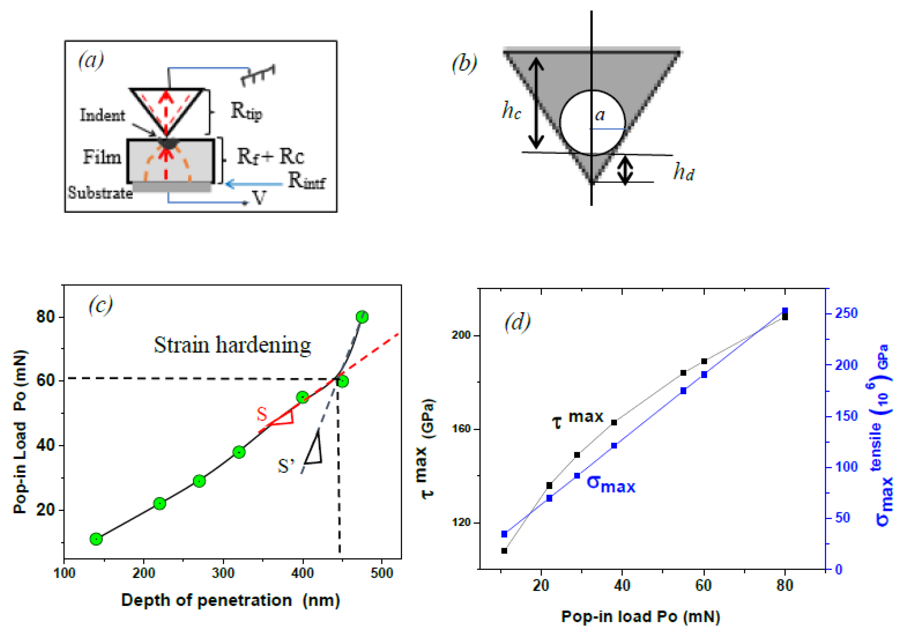
Conduction between the indenter tip and sample surface requires the application of an external bias in the current direction, as shown in Figure 3a. The resistances that are impacted by indentation and any associated phenomena are the contact resistance Rf and the constriction resistance (RC) [14,15]. The resistance at the coating/substrate interface Rintf, which may not be active at shallow depths of indentation (less than 10% thickness), is the resistance component that is affected subject to mechanical stimulation delivered by the indenter in addition to Rc specifically for a film/substrate system.
Nanoindentation performed on TiB2 films on silicon substrate showed fracture events as represented through the pop-in in the load-depth plot. The maximum shear stress, τmax, and the maximum tensile stress (σmaxtensile ) induced during the indentation process at the point of pop-in are given as eq 4 and 5 [16]
τ m a x = 0.31   6 E r 2 π 3 R 2 P o 1 / 3
σ m a x t e n s i l e   = ( 1 2 ν ) P o 2 π a 2
where R is the tip radius, Po is the pop-in load, Er is the reduced modulus and a is the contact radius at the pop-in. The period for which the fracture (pop-in) took place was estimated to be about 10 s. The impulse (ΔP/Δt) which caused the fracture was 0.02 mN/s. This impulse usually sends shock waves into the films and can hamper any conduction process taking place between the tip and the sample. The pop-in event is the onset of inelastic deformations and competition between dislocation-induced plasticity (by τ max) and crack formation (σmax tensile) which depends on the stress beneath the indenter tip. For sharper indenters, dislocation plasticity occurs prior to crack formation. The pop-in loads obtained from Figure 2h showed steady increase with penetration depth initially and an increase at the later stages caused by strain hardening due to new dislocations formed in the plastic zone of radius rp beneath the indentation as per eq 6 (Figure 3c) [17]. The onset of strain hardening is at 65 mN with a corresponding penetration depth of 450 nm gives the yield stress as (σy= Pomax/24.5 hmax2) 13 GPa. The plastic radius comes out as 1.54 μm which is the similar dimension of the coating thickness, indicating the strain hardening is taking place in the coating with no substrate influence. The change in stiffness (ΔS=S-S=4.8 μN/m) as indicated in the figure divided by rp gives a value of 3Pa as the flow stress existing in the plastic zone. The maximum nominal shear and tensile stress were proportional to the increasing pop-in load with penetration (Figure 3d)
r p = 3 P 2 π   σ y   ; σ y   =   13   GPa

4. Conclusions

High precision indentation is significant in terms of understanding the material response to external mechanical stimuli, useful for their application in device fabrication and as protective coatings for industrial tools. A change in tip-sample contact from Hertzian at shallow depths of penetration to pyramidal at larger depths was found to bring about ductile to brittle transitions involving internal crack generation. The indentation performed at higher loads of penetration showed the formation of radial, secondary radial, and picture frame cracks. The crystalline nature of the TiB2 films had roles to play in resisting indentations at shallow depths as well as in radial crack deflection. The electrical conduction paths were defined on the indentation impressions. The cracking phenomenon seems to generate additional conduction paths. However, crack branching will again enhance the resistance showing the importance of nanocrystalline thin film growth features essential for preventing electro-mechanical failures in microelectronic device fabrication.

Acknowledgements

The authors would like to acknowledge Dr. S. K. Mishra, CSIR-National Metallurgical Laboratory, and Dr. P. K. P. Rupa, Tripura University for experimental facilities.

Conflict of Interest

The authors have no conflicts to disclose.

References

  1. Rupa, P.K.P.; Chakraborti, P.C.; Mishra, S.K. Mechanical and deformation behavior of titanium diboride thin films deposited by magnetron sputtering. Thin Solid Films 2009, 517, 2912–2919. [Google Scholar] [CrossRef]
  2. Ritambhara Dash, A. S. Bhattacharyya Crack growth based on indentation along substrate and nanocrystallites in Titanium diboride thin films. Fatigue & Fracture of Engineering Materials & Structures 2023. [Google Scholar] [CrossRef]
  3. Li, X.; Bhushan, B. A Review of Nanoindentation Continuous Stiffness Measurement Technique and Its Applications. Mater Charac. 2002, 48, 11–36. [Google Scholar] [CrossRef]
  4. Yu, N.; Polycarpou, A.A. Use of the focused ion beam technique to produce a sharp spherical diamond indenter for sub-10 nm nanoindentation measurements J. Vac. Sci. Technol. B 2004, 22.2., 668–672. [Google Scholar] [CrossRef]
  5. Wang, D.; Lu, X.; Lin, M.; Wan, D.; Li, Z.; He, J.; Johnsen, R. Understanding the hydrogen effect on pop-in behavior of an equiatomic high-entropy alloy during in-situ nanoindentation. Journal of Materials Science & Technology 2022, 98, 118–122. [Google Scholar]
  6. Lu, X.; Ma, Y.; Peng, D.; Johnsen, R.; Wang, D. In situ nanomechanical characterization of hydrogen effects on nickel-based alloy 725 under different metallurgical conditions. Journal of Materials Science & Technology 2023, 135, 156–169. [Google Scholar]
  7. Gouldstone, H.-J.; Koh, K.-Y.; Zeng, A.E. Giannakopoulos, S. Suresh, Discrete and continuous deformation during nanoindentation of thin films. Acta Materialia 2000, 48, 2277–2295. [Google Scholar] [CrossRef]
  8. Guillonneau, G.; Wheeler, J.; Wehrs, J.; Philippe, L.; Baral, P.; Höppel, H.; Michler, J. Determination of the true projected contact area by in situ indentation testing. Journal of Materials Research 2019, 34, 2859–2868. [Google Scholar] [CrossRef]
  9. Chen, J. Indentation-based methods to assess fracture toughness for thin coatings. J. Phys. D: Appl. Phys. 2012, 45, 203001. [Google Scholar] [CrossRef]
  10. Stefano, G. Electrical Behaviour of a Single Crack in a Conductor and Exponential Laws for Conductivity in Micro Cracked Solids. 2007, 1, 1–19. [Google Scholar]
  11. Rebouta, L.; Rubio-Pena, L.; Oliveira, C.; Lanceros-Mendez, S.; Tavares, C.J.; Alves, E. Thin Solid Films 2010, 518, 4525–4528. [CrossRef]
  12. Leterrier, Y.; Pinyol, A.; Rougier, L.; Waller, J.H.; Manson, J.-A.E. J. Appl Phys. 2009, 106, 113508.
  13. Glushko, O.; Kraker, P.; Cordill, M.J. Explicit relationship between electrical and topological degradation of polymer-supported metal films subjected to mechanical loading. arXiv:1904.03007. [CrossRef]
  14. S.C-Dassonneville, F.Volpi et al. MRS Comm. Resistive-nanoindentation: contact area monitoring by real-time electrical contact resistance measurement. 2019, 9, 1008–1014.
  15. Dash, R.; Bhattacharyya, K.; Bhattacharyya, A.S. Nano. Prec. Eng. 2023, 6. [Google Scholar]
  16. Fang, X.; Bishara, H. Nanoindentation pop-in in oxides at room temperature: dislocation activation or crack formation? J Am Ceram Soc. 2021, 104, 4728–4741. [Google Scholar] [CrossRef]
  17. Zak, S. , Trost, C.O.W., Kreiml, P. et al. Accurate measurement of thin film mechanical properties using nanoindentation. Journal of Materials Research 2022, 37, 1373–1389. [Google Scholar] [CrossRef]
Figure 1. a) Load-depth (P-h) plot for nanoindentations done for 50 and 100 nm (b) SEM image tip bluntness (reproduced with permission) [4] (c) schema of zero-point correction and the changing nature of contact-generating cracks with increased depth of penetration.
Preprints 91367 g001
Figure 2. (a) Palmqvist-radial, secondary-radial, picture frame, and through-thickness cracks can be observed originating from different regions of the nanoindentation impression. The dotted line showing indentation contact edges deviated from a geometrically perfect shape. (b) Schema of the cracking phenomena (c) crystallite density with approximately 30 nanocrystallites in an area of 6.25 µm2 (d) conduction paths originating in the indentation (e) deviation in crack propagation (f, g) plots of relative resistance (R/Ro) with crack length (Cl) and Crack Factor (CF) (h) Variation of P–h and Slope vs. depth (inset) for TiB2-Si (reproduced with permission [1,2]).
Preprints 91367 g002
Figure 3. (a) Electrical conduction between indenter tip and sample with different resistances [14,15] b) Geometry of a blunt indenter (c) variation of pop-in load (Po) with the depth of penetration (d) the maximum shear stress, τmax, and the maximum tensile stress (σmaxTensile).
Preprints 91367 g003
Table 1. The variations in crack length, crack factors for different types of films failures affecting the relative resistance of the films.
Crack no. Type Length (µm) CF R/Ro
1 Radial crack 4.5 1.35 2.85
2 Radial crack 7 2.1 4.67
3 Picture frame crack 4 1.2 2.57
4. Secondary radial crack 2 0.6 1.60
5. Picture frame crack 3 0.9 2.05
6. Internal ductile
Fracture (multiple)
3.5 (average) 1.05 2.29
7. Internal ductile fracture 1.5 0.45 1.42
8. Picture frame 1 0.3 1.25
9. Internal ductile
fracture
2.5 0.75 1.81
Disclaimer/Publisher’s Note: The statements, opinions and data contained in all publications are solely those of the individual author(s) and contributor(s) and not of MDPI and/or the editor(s). MDPI and/or the editor(s) disclaim responsibility for any injury to people or property resulting from any ideas, methods, instructions or products referred to in the content.
Copyright: This open access article is published under a Creative Commons CC BY 4.0 license, which permit the free download, distribution, and reuse, provided that the author and preprint are cited in any reuse.
Prerpints.org logo

Preprints.org is a free preprint server supported by MDPI in Basel, Switzerland.

Subscribe

© 2024 MDPI (Basel, Switzerland) unless otherwise stated