1. Introduction
Active magnetic bearings (AMBs) utilize a magnetic field to suspend a rotor whose relative position is actively monitored and corrected by a controller. AMBs offer a competitive advantage in high-speed rotating machines, vibration isolation and high precision machining applications due to their contactless nature and ability to control and monitor the rotor position (Schweitzer and Maslen, 2009). Recent research has focused on the actuation and control subsystems of AMBs. Force generated by AMBs has a nonlinear relationship with the supplied coil current. AMBs are inherently unstable due to the attractive nature of electromagnets. Therefore, there is a need for a controller to stabilize the system.
Most industrial AMBs rely on a current control strategy which requires amplification of the command signal from the controller to a control current which is fed to the coils. Switching power amplifiers (SPAs) are the most preferred in the current control scheme because of their improved efficiency over the linear power amplifiers (LPAs) (Tonoli, et al., 2012). The application of metal-oxide-semiconductor field effect transistors (MOSFETs) based switching power amplifiers for current control has been well studied over time with suggested improvements from different researchers. Gallium nitride transistors (GaNT) based SPA have been suggested for a wide bandwidth and high switching frequency for the current control scheme (Hu, et al., 2023). GaN are a new type of power electronics component which tend to have lower switching thresholds and better on-state resistance than traditional MOSFETs (Hu, et al., 2023). Utilization of the wide bandwidth and high switching frequency lowers the current ripple and improves performance. For a better current response and reduced current ripple simultaneously, researchers suggested a dual mode power drive system, 2-level pulse width modulation and 3-level pulse width modulation techniques (Chiu and Tsai, 2019), (Yu, et al., 2020), and (Rao, et al., 2023).
However, many suggested improvements on the current control SPAs increase the complexity of the electronic circuitry of the AMBs (Hu, et al., 2023). To eliminate the limitations of MOSFET bandwidth, and its low switching frequency together with the additional circuit subsystem of a current control scheme, a voltage control scheme utilizing the superior characteristics of GaN is suggested. To evaluate the performance of GaN in a voltage control scheme for AMBs, an experimental comparison between GaN and MOSFET for voltage controlled active magnetic levitation was performed.
This paper presents a comparison of the performance of GaN and MOSFET in a voltage-controlled scheme for active magnetic bearings. An experimental study is carried out using GaN on an AMB and compared with MOSFETs on the same AMB. The current, voltage, and position of the ferromagnetic target is monitored for each case and the results compared. A position setpoint step response Is performed with the GaN and the MOSFET. The overall system performance is evaluated from the results obtained. With the GaN posing higher switching frequency, with a wider bandwidth and reduced switching losses, a superior performance is expected.
This paper is structured as follows. The next section presents the basic ideas of voltage control for AMB levitation and compares it to the more common current control method. Also, a brief introduction to GaN and how they compare to MOSFETs is covered. Then,
Section 3 details the experimental test rig used to compare GaN to MOSFETs for single axis levitation. Experimental levitation results are presented in
Section 4 using both types of transistors. Finally, some closing remarks are made in
Section 5.
2. Theory
2.1. Voltage Control for Levitation
The basic force function for active magnetic levitation is shown in Eq (1). The first term is positive and is for upward force of a top electromagnet. The second term is negative for the downward force of the opposing electromagnet.
The parameters
μ0 (permeability of free space),
A (pole area),
N (number of coil windings),
ib (bias current), and
g (nominal air gap) can be considered as constants.
x is the position of the ferromagnetic target rotor measured from the center of the bearing. For ease of analysis, the force equation is usually linearized at the operating point in terms of the control variables, current and position.
The levitation problem is inherently unstable; as the rotor rises, the upward force increases, etc. For stable levitation, the control current ic must be changed in real time to compensate for rotor deflections. This leads to the natural conclusion to control coil current as a feedback of rotor position.
However, current in the coil cannot be dictated directly. It has its own dynamics, even at its simplest, neglecting back emf and other effects:
Here, applied voltage
v induces change in coil current but that is mitigated by resistance
R and inductance
L. To achieve desired current, and therefore desired levitation force, a servo amplifier is often utilized which has its own current sensor and feedback control law which can automatically account for electrical disturbances or changes in load. The desired current is set by the levitation controller in an outer control loop. That desired current serves as the set point for the inner control loop. This common AMB levitation strategy is illustrated in
Figure 1a.
The inner current control loop must be faster than the outer levitation control loop, ideally by at least an order of magnitude. Communication from the levitation controller to the current controller, which may be digital or analog, may reduce controller bandwidth. And, the servo amplifier is often expensive. Voltage control for levitation can be implemented without these issues.
A simple form of voltage control for AMB levitation is illustrated in
Figure 1b. Here, the rotordynamics, AMB force function, and coil dynamics are considered as a single plant. The control input to that plant is voltage which can be implemented readily as an equivalent analog with a fast-switching transistor. When the transistor is switched on or off, the suddenly applied voltage induces a transient current in the load. By varying the percentage of time the voltage is switched on, the so-called duty cycle, to that of the total of a fixed switching frequency current can be made to oscillate about a relative level. If the switching frequency is high compared to the plant dynamics, the current signal may be approximated as an analog signal. Because of this strategy, the switching characteristics of the transistor can be significant to the efficiency of the implementation. The next section compares the general switching characteristics of MOSFETs and GaNTs.
2.2. GaNs vs MOSFETs
Nowadays, power electronics require more power, more efficiency, and greater capacity for miniaturization. Also, new devices require operation at higher frequencies. However, operation at higher frequencies will mean greater losses on switching elements (Boutros, et al. 2013).
Currently, machines using power electronics rely almost exclusively on silicon-based power devices which is a well- established technology. However, every day, the power requirements keep growing at a high rate, while power electronic devices make incremental advances to the mature technology. On the other hand, high efficiency applications require low stand-by current, fail-safe devices with high current/voltage capability, and minimum cooling (Ma, 2019).
GaNTs appeared as a disruptive technology that will replace MOSFET in the mid-term future. In fact, GaN switches are projected to have a 100× performance advantage over silicon-based devices and 10× over SiC (Boutros, et al. 2013). Some of the main advantages of GaN over silicon devices are the breakdown voltage it can support, and the specific on- resistance value it can reach (Meneghini, et al., 2017). The construction properties of GaN enable it to have high theoretical value of
VB2/
Ron,sp = 5000 MW/cm
2 (
VB is breakdown voltage and
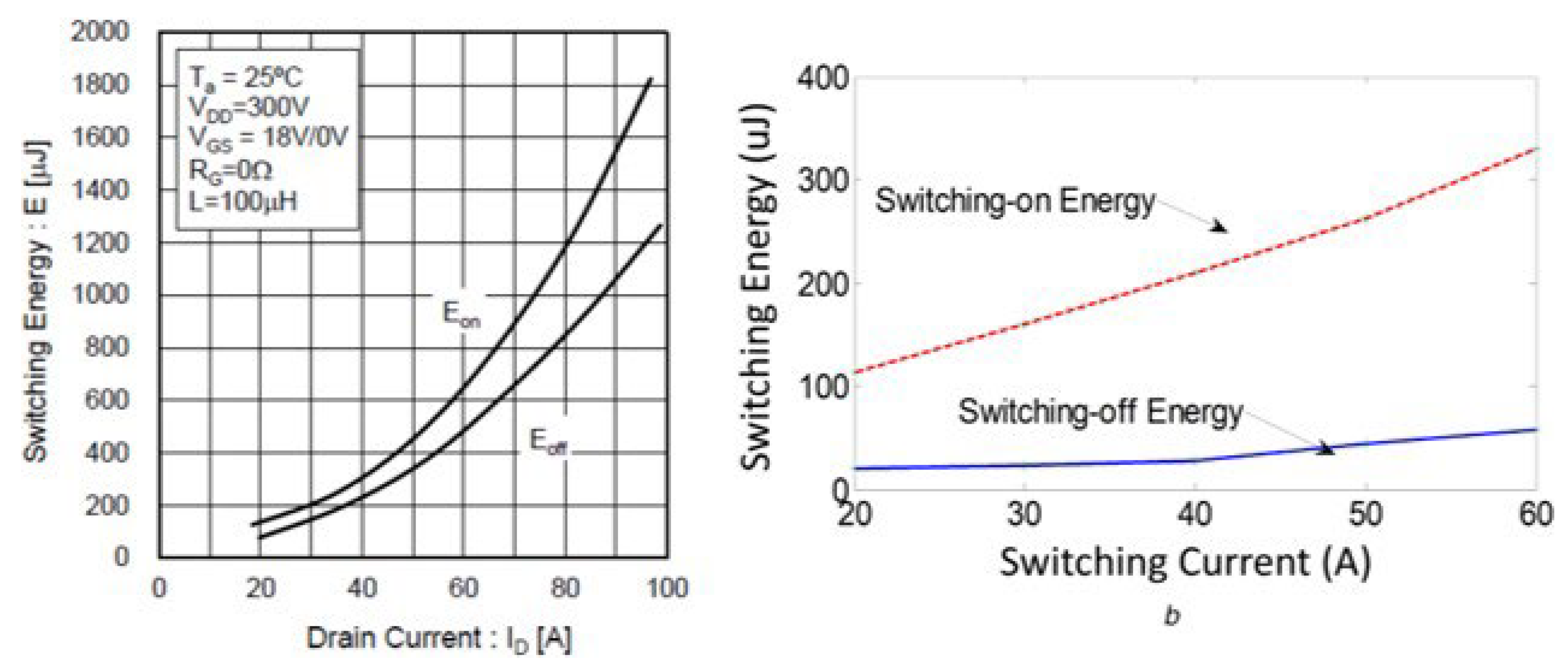
Ron,sp is resistance) compared to 40 for Si super-junction MOSFETs and 640 for SiC. These advantages allow GaN to reach higher off voltages without facing temperature issues. Also, it enables the heat sink to be smaller than one used for a MOSFET in an equivalent application. Another advantage of GaN devices is the high saturated drift velocity, which allows operation at more than 10× the switching frequency of Si devices with the same switching loss. Operating at 10× higher frequency allows reduction of the size of passive components, contributing to the miniaturization of power machines (Ma, 2019). In
Figure 2, switching losses of SiC device and GaN are compared. It can be noticed that energy consumption using GaNTs is more efficient at higher frequencies.
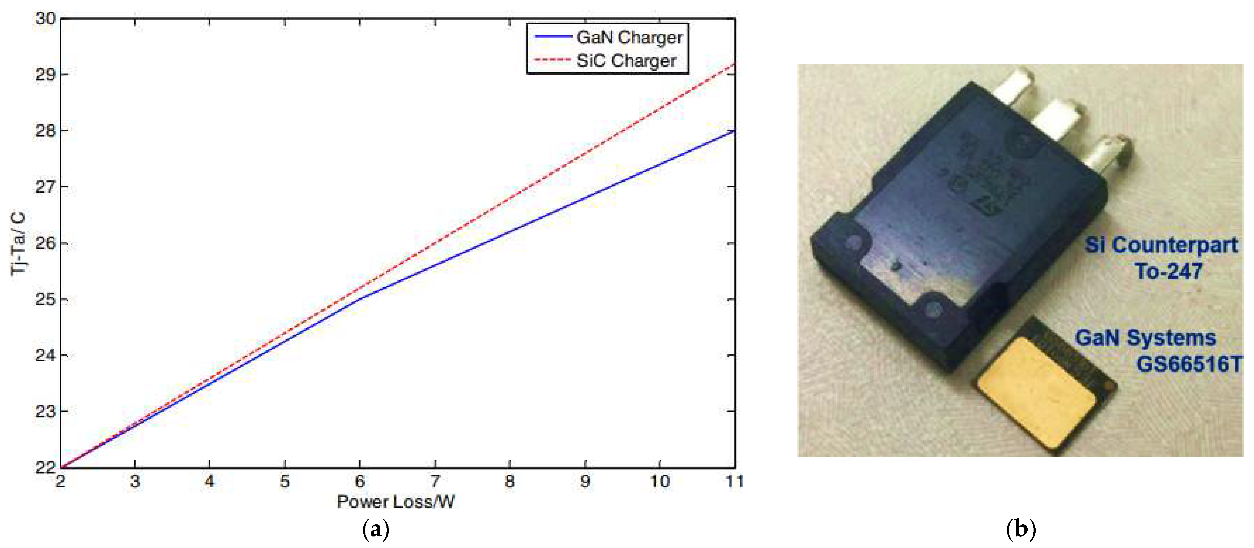
In (Lui, et al., 2017), a thermal comparison between SiC MOSFET (SCT3022AL) and GaNT (GS66516T) was performed. A DC current was flown through the GaN device. The product of this current and voltage across the transistor represents the power loss. At the same time, two thermistors were attached to the transistor and to an affixed heat sink. The same experiment was performed with the MOSFET device. As a result,
Figure 3a shows the measured temperature.
For the GaNT, the measured temperature reached 0.62
oC/W. In contrast, MOSFET devices yielded 0.8
oC/W. In terms of gate-drive power, SiC MOSFET consume more than GaNT, given a higher gate-drive voltage and gate charge. Therefore, at higher switching frequencies the MOSFET’s power dissipation will be greater (Lui, et al., 2017). In terms of size, GaN devices are much smaller than SiC MOSFET silicon devices.
Figure 3b shows the relevant size difference of these devices with similar capabilities (Lui, et al., 2017).
3. Experimental Test Rig
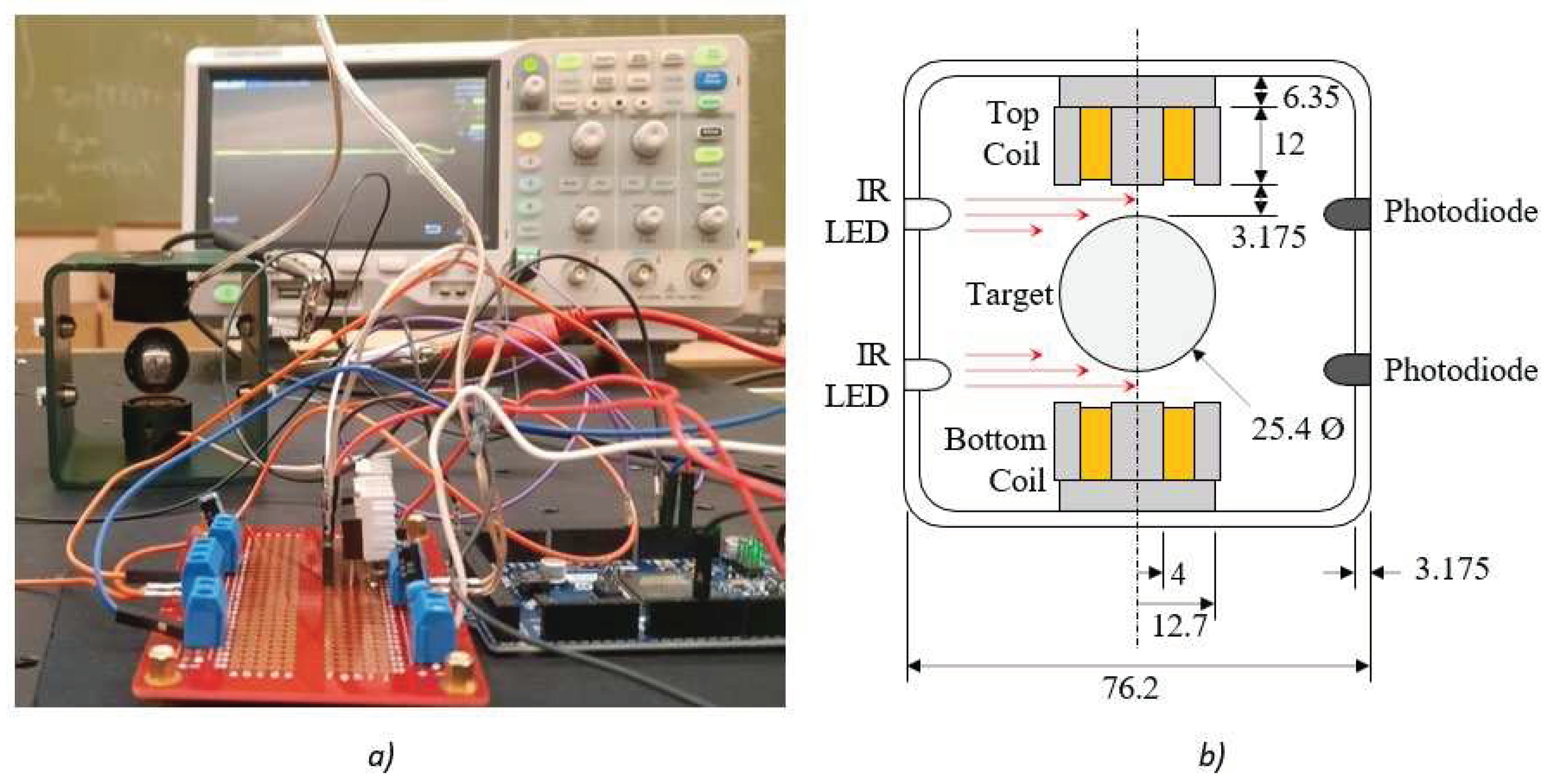
The test rig is made up of a 76.2 mm by 76.2 mm by 76.2 mm steel housing. One electromagnet is attached to the bottom of the housing, and another attached to the top. A rotor is suspended between the electromagnets leaving an airgap of 3.175 mm from the top and bottom electromagnet. The two electromagnets used for the construction of the test rig had 480 turns. Each electromagnet was covered with a steel ring around them to control the magnetic fields minimizing the losses of the magnetic force generated. The electromagnets were powered by a 7 VDC supply. To control the airgap, 6.35 mm thick spacers were used. The parameters of the 1 DoF magnetic levitation test rig are shown in
Table 1.
Two infrared sensors are attached to the side of the casing to actively monitor the position of the rotor. The sensors have two emitters on one side and two detectors on the opposite side. They are powered by 3.3V supplied by an Arduino Due. The sensors convert the position of the rotor to an analog voltage signal. The analog voltage signal is input into the 12-bit ADC of the microcontroller for quantization and conversion into a digital signal for processing. The sensors were manually calibrated about the operating point to establish the set point and the relationship between the position and voltage signal which helped implement the control law.
Figure 4 shows a photograph and sketch of the experimental test rig.
An ARM Cortex-M3 processor is used to implement the voltage control law. The signal is converted to a digital signal and compared with the calibrated setpoint. The error signal generated from this comparison is fed into a PID controller algorithm for generation of a control signal. A pulse width modulated (PWM) control signal is generated from the controller. The control signal through the MOSFETs or GANT, modulates the voltage supplied to the electromagnetic coils. The different properties of MOSFET and GANT are exploited, and their performance compared.
EPC 2100 GaN and PHP191NQ06LT MOSFET were used for the purpose of this experiment. The first experiment was performed using the GaN transistors and the second one used MOSFET transistors. Both type of transistors receives a PWM signal from the controller and switch to deliver power to the magnets. The specific characteristics of MOSFET and GaN determine the level of noise attenuation, current ripple suppression, and power losses which improves the stability and dynamic performance of the system.
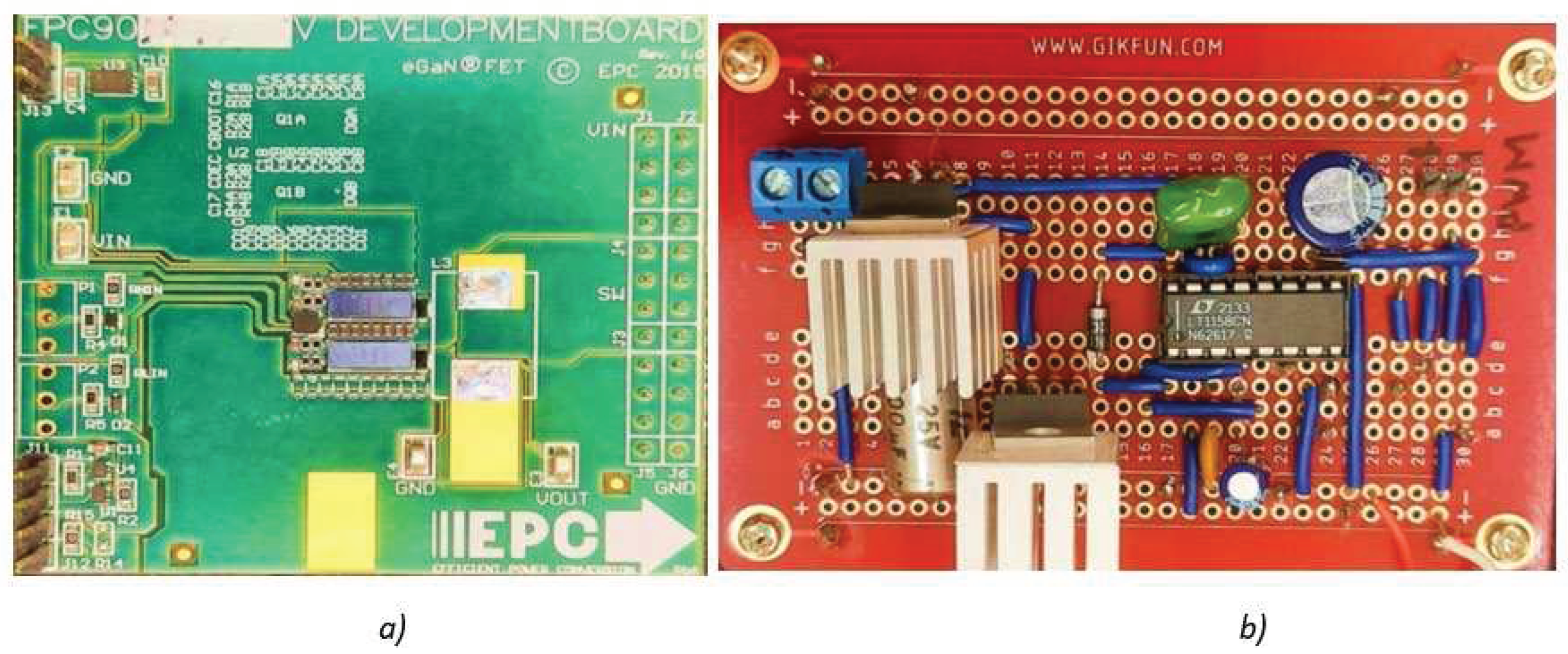
For GaNT implementation, a purchased EPC9059 development board was used. This board contains EPC2100 GaN transistors connected in half-bridge inverter topology. On the other hand, a board for MOSFETs was built to have a similar electrical design. Both transistor boards are shown in
Figure 5. For data acquisition, KEYSIGHT N7026A current probe and KEYSIGHT MSOX4054A Oscilloscope were used.
4. Experimental Results
A levitation experiment was run with the GaN and MOSFET boards. For both tests, drain-source voltage 𝑉𝑑𝑠 and drain-source current 𝐼𝑑𝑠 of the top coil transistor were measured. By using this data, switching and conduction losses were estimated. For switching losses analysis, opened to closed and closed to opened transitions were compared for the GaNT and MOSFET. On the other hand, for conduction losses analysis, the dissipated energy is estimated when the transistor is closed.
Switching losses analysis: The energy of a signal is taken as the sum of the power over the switching time. Power is taken as the product of voltage drop across and current through the transistor for the top levitation coil. For one period of the voltage applied to the magnet, there is one closed to opened transition and one opened to closed transition.
Conduction losses analysis: Conduction power losses are estimated by the current squared multiplied by the transistor resistance from the drain to source and the duty cycle. For MOSFET and GaNT, the results will be analyzed for the same duty cycle.
4.1. Levitation using MOSFET
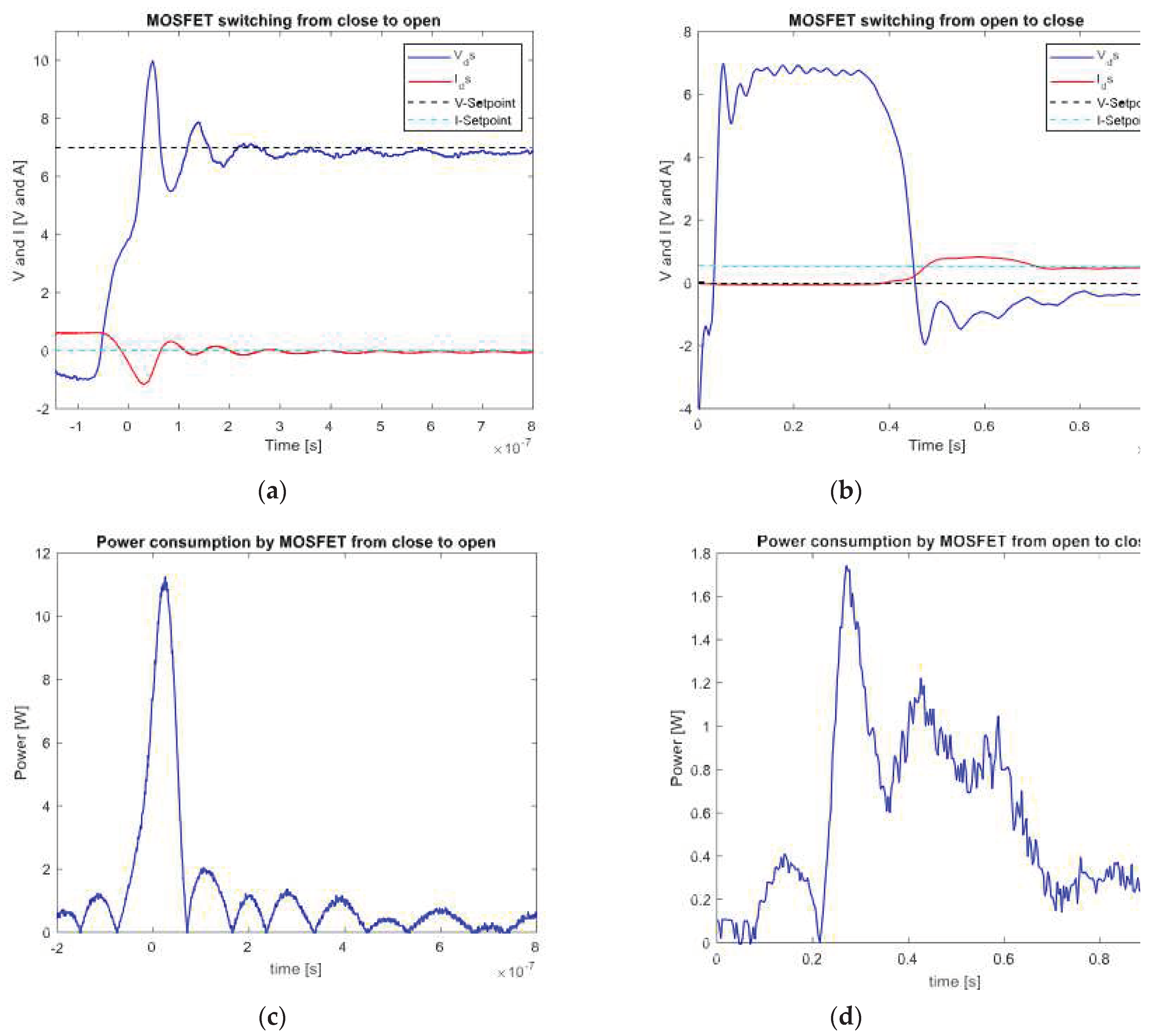
With PWM switching at 1 kHz, the closed to opened transition takes around 0.39 μs to settle. The power losses are observed in
Figure 6. The dissipated energy in the 0.39 μs of switching from closed to opened is 3.21 μJ. For opened to closed transition, it takes 0.48 μs to settle. Also, the dissipated energy in this period is 0.21 μJ. The voltage, current, and power consumption for the MOSFET switching open and closed during levitation are shown in
Figure 6.
For conductive losses analysis, the drain to source resistance is 75 mΩ. The steady stae current is 0.46 A. Therefore, the power losses with a duty cycle of 41.94% reach are 6.65 mW.
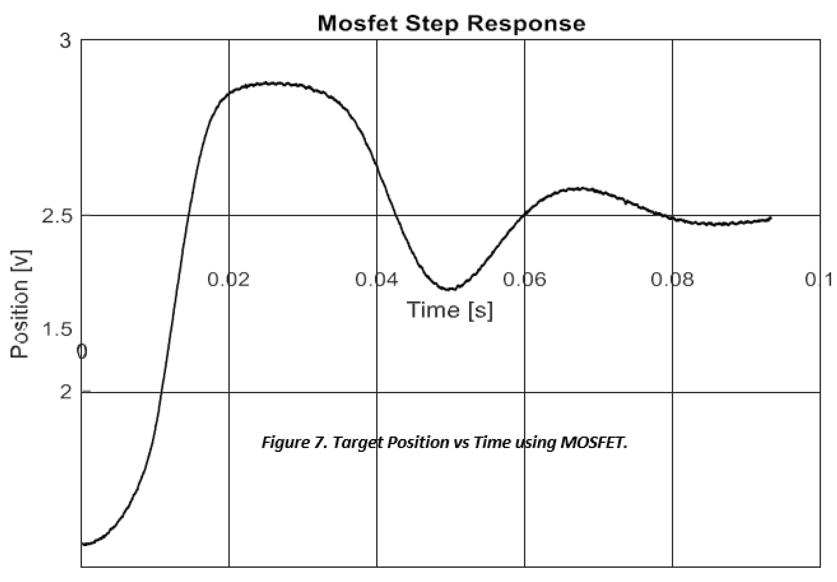
A position step response is performed during levitation while using the MOSFET resulting in a 48% overshoot with 0.0241 s peak time. The settling time for the step response was 0.12 s with a steady state error of 0.03 V as shown in
Figure 7.
4.2. Levitation using GaNT
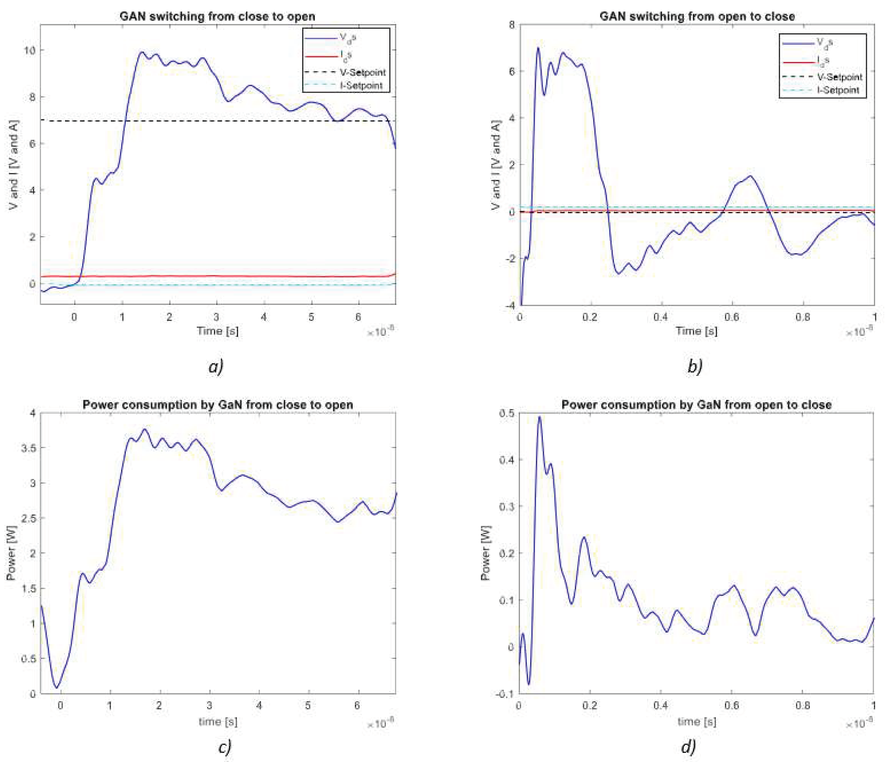
The levitation experiment is repeated using the GaNT, all else being equal. Running at 1 kHz, the closed to opened transition takes around 70.46 ns to settle. The power losses are observed in
Figure 9. The dissipated energy in 70.46 ns of switching from closed to opened is 0.58 μJ. For opened to closed transition, it takes 0.17 μs to stabilize. Also, the dissipated energy in this period is 3.29 nJ. The voltage, current, and power consumption for the MOSFET switching open and closed during levitation are shown in
Figure 8.
For conductive losses analysis, the drain to source resistance is 51 mΩ. The steady state current is 0.28 A. Therefore, the power losses with a duty cycle of 41.94% reach are 1.67 mW.
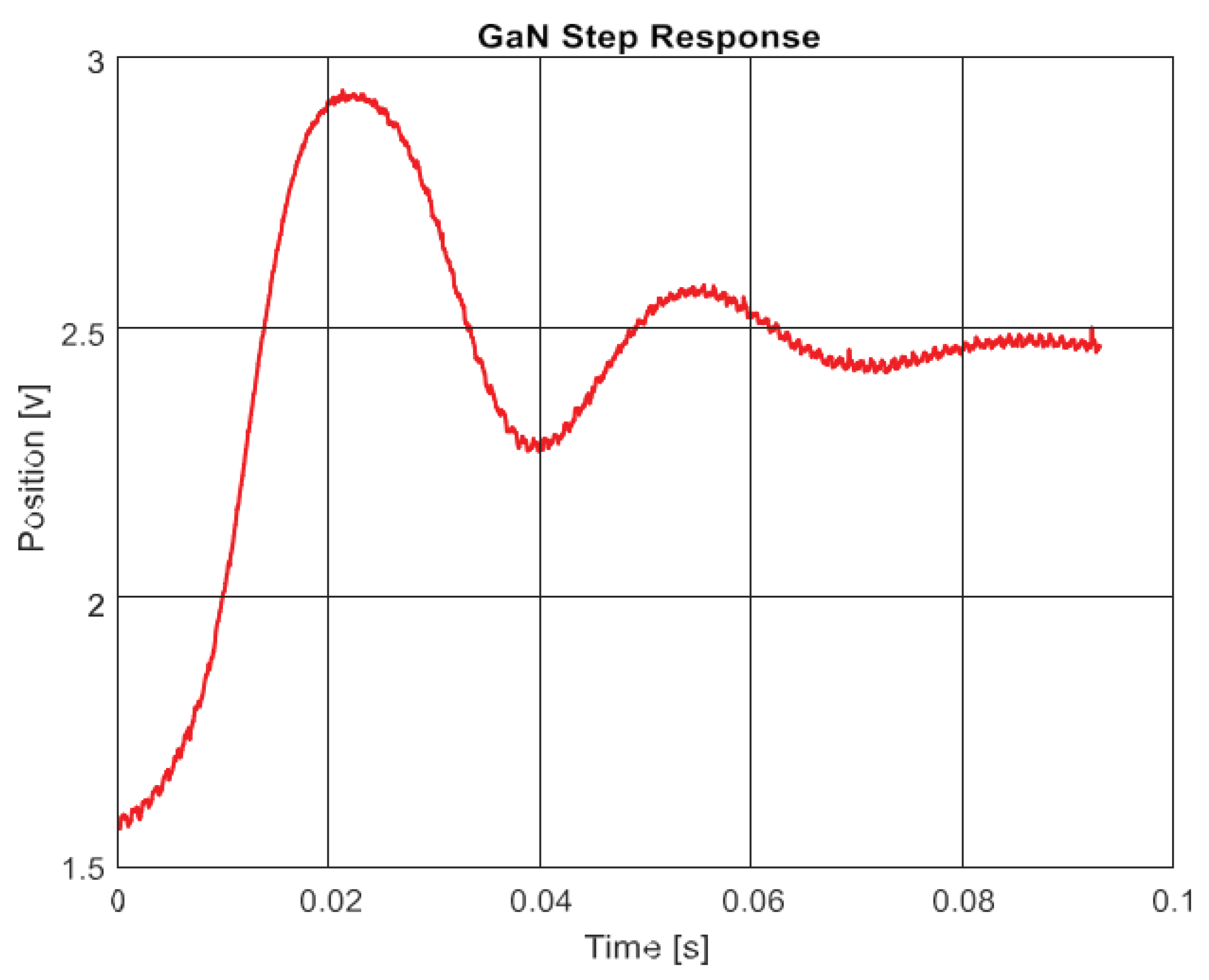
The step response obtained while using the GaN transistors had a 51% overshoot with 0.0212 s peak time. It took 0.0127 s to settle with a 0.02 V steady state error as shown below in
Figure 9. This step response has higher overshoot than that when using the MOSFET. This indicates higher actuator gain and therefore higher closed-loop stiffness leading to lower equivalent damping ratio. Recall that the PID levitation controller is held constant between transistor trials. The higher actuator gain is also leading to a slightly higher natural frequency. Therefore, the use of the GaNT enables the opportunity for renewed controller optimization.
4.3. Results Summary
Table 2 summarizes the performance of the MOSFET and GaNT during the 1 DoF levitation tests. Overall, the GaNT exhibited lower losses and faster switching time than the MOSFET during levitation.
5. Conclusions
GaNTs are a relatively new type of power transistor compared to MOSFETs. This work experimentally compared the performance of a GaNT to a MOSFET for a simple 1DoF PWM voltage controlled magnetic levitation test rig. Transistor current, voltage, switching time, and levitation target position were measured for static levitation and a position step response. It was found that the GaNT had faster response time and less losses than the MOSFET.
The more wide spread application of GaNT power electronics to AMBs will lead to AMBs being more efficient and competitive with other types of bearings. Also, the higher actuator gain can enable better AMB performance and the smaller size and less heat generation of GaNTs can lead to more convenient AMB control hardware further increasing the marketability of AMBs.
This study should be repeated for a fully levitated rotor at speed and can be improved by the addition of heat generation measurements.
References
- Boutros, K, Chu. Recent Advances in GaN Power Electronics. IEEE 2013 Custom Integrated Circuits Conference, San Jose, CA, USA, 22-25 September 2013. [Google Scholar]
- Chiu, HL, and Tsai. Dual-Mode Power Drive for Active Magnetic Bearings. IET Electr Power Appl. 2019, 13, 162–167. [Google Scholar] [CrossRef]
- Hu, HJ, Liu. A Wide Bandwidth GaN Switching Power Amplifier of Active Magnetic Bearing for a Flywheel Energy Storage System. IEEE Trans Power Electron 2023, 38, 2589–2605. [Google Scholar] [CrossRef]
- Liu, G, Bai. Comparison of SiC MOSFET-based and GaN HEMT- based high-efficiency high-power density 7.2 kW EV Battery Chargers. In: , Albuquerque, NM, USA, IEEE 5th Workshop on Wide Bandgap Power Devices and Applications, Albuquerque, NM, USA, 11 December 2017. [Google Scholar]
- Ma, B. Driving GaN Power Transistors. 31st International Symposium on Power Semiconductor Devices and ICs, Shanghai, China, 19-23 May 2019; 23 May 2019. [Google Scholar]
- Meneghini, M, Rossetto. Reliablity and Failure Analysis in Power GaN-HEMTs: an Overview. IEEE International Reliability Physics Symposium, Monterey, CA, USA, 2-6 April 2017. [Google Scholar]
- Rao, JS, Arun. Lecture Notes in Mechanical Engineering. Available online: http://www.springer.com/series/11693 (accessed on 6 May 2023).
- Schweitzer G and Maslen EH, (eds) (2009) Magnetic Bearings: Theory, Design, and Application to Rotating Machinery.
- Heidelberg. Springer Verlag Publishers.
- Tonoli A, Bonfitto, A. Rotors on Active Magnetic Bearings: Modeling and Control Techniques. In Advances in Vibration Engineering and Structural Dynamics; Beltran-Carbajal, F (eds), Ed.; IntechOpen: Rijeka, 2012; pp. 1–28. [Google Scholar]
- Yu, Z, Gong. Duty Ratio Stability and Average Steady-State Error of Two-Level Current-Mode Wide Bandwidth Switching Power Amplifiers. IEEE Trans Power Electron 2020, 35, 4094–4104. [Google Scholar] [CrossRef]
Figure 1.
AMB Control Schemes, a) Typical Current Control, and b) Simple Voltage Control used in the Current Study.
Figure 1.
AMB Control Schemes, a) Typical Current Control, and b) Simple Voltage Control used in the Current Study.
Figure 2.
Double-pulse-test results of SiC and GaN a) DPT results of SiC MOSFETs (SCT3022AL), b) DPT results of GaN HEMTs. (GS66516T) (Liu, et al., 2017).
Figure 2.
Double-pulse-test results of SiC and GaN a) DPT results of SiC MOSFETs (SCT3022AL), b) DPT results of GaN HEMTs. (GS66516T) (Liu, et al., 2017).
Figure 3.
a) Experimental curve of the GaN thermal resistance, b) Size of Si and GaN counterparts (Liu, et al., 2017).
Figure 3.
a) Experimental curve of the GaN thermal resistance, b) Size of Si and GaN counterparts (Liu, et al., 2017).
Figure 4.
Experimental Test Rig, a) Photograph, and b) Sketch, dimension in mm.
Figure 4.
Experimental Test Rig, a) Photograph, and b) Sketch, dimension in mm.
Figure 5.
Power boards, a) EPC9059 GaN development board, and b) MOSFET board based on PHP191NQ06LT.
Figure 5.
Power boards, a) EPC9059 GaN development board, and b) MOSFET board based on PHP191NQ06LT.
Figure 6.
Switching in MOSFET, a) 𝑽𝒅𝒔and 𝑰𝒅𝒔 in closed to opened switching, b) 𝑽𝒅𝒔 and 𝑰𝒅𝒔 in opened to closed switching, c) power losses in closed to opened switching, and d) power losses in opened to closed switching.
Figure 6.
Switching in MOSFET, a) 𝑽𝒅𝒔and 𝑰𝒅𝒔 in closed to opened switching, b) 𝑽𝒅𝒔 and 𝑰𝒅𝒔 in opened to closed switching, c) power losses in closed to opened switching, and d) power losses in opened to closed switching.
Figure 7.
Target Position vs Time using MOSFET.
Figure 7.
Target Position vs Time using MOSFET.
Figure 8.
Switching in GaN, a) 𝑽𝒅𝒔and 𝑰𝒅𝒔 in closed to opened switching, b) 𝑽𝒅𝒔 and 𝑰𝒅𝒔 in opened to closed switching, c) power losses in closed to opened switching, and d) power losses in opened to closed switching.
Figure 8.
Switching in GaN, a) 𝑽𝒅𝒔and 𝑰𝒅𝒔 in closed to opened switching, b) 𝑽𝒅𝒔 and 𝑰𝒅𝒔 in opened to closed switching, c) power losses in closed to opened switching, and d) power losses in opened to closed switching.
Figure 9.
Target position vs Time using GaNT.
Figure 9.
Target position vs Time using GaNT.
Table 1.
Test Rig Parameters.
Table 1.
Test Rig Parameters.
| parameter |
Description |
Value |
| m |
Levitated mass |
0.02 kg |
| ki |
Force –current factor |
0.914 N/A |
| kx |
Force – displacement factor |
750.9 N/m |
| L |
Inductance |
8.85×10⁻³ H |
| R |
Resistance |
3.87 Ω |
| g |
Nominal airgap |
3.175×10⁻³ m |
| N |
Number of turns |
480 |
| Vs |
Supply voltage |
9 V |
Table 2.
Summary of Transistor Performance.
Table 2.
Summary of Transistor Performance.
| Measure |
MOSFET |
GaNT |
| Switching Losses – Closed to Open |
3.21 μJ |
0.58 μJ |
| Switching Losses – Open to Closed |
0.213 μJ |
3.287 nJ |
| Switching Time – Closed to Open |
0.392 μs |
70.47 ns |
| Switching Time – Open to Closed |
0.48 μs |
0.17 μs |
| Conductive Losses |
6.65 mW |
1.67 mW |
|
Disclaimer/Publisher’s Note: The statements, opinions and data contained in all publications are solely those of the individual author(s) and contributor(s) and not of MDPI and/or the editor(s). MDPI and/or the editor(s) disclaim responsibility for any injury to people or property resulting from any ideas, methods, instructions or products referred to in the content. |
© 2024 by the authors. Licensee MDPI, Basel, Switzerland. This article is an open access article distributed under the terms and conditions of the Creative Commons Attribution (CC BY) license (https://creativecommons.org/licenses/by/4.0/).

