1. Introduction
Moore’s Law is a prediction and observation made by Gordon Moore, founder of Intel, that number of transistors in the microchip will double every two years. This will lead to exponential increase in computing power, while the per unit transistor cost will decrease. This has been achieved due to rapid advances in design and manufacturing technologies in past. The trend told by this law is how computational power scaling has been grown for decades. But this law has reached its end.
Future transistor scaling is impossible as we have reached the physical limits of reducing the size of transistors[
1,
2]. High-end modern day silicon are made up of billions of transistors and each transistor is made up of only a few atoms. Moreover, we can see in
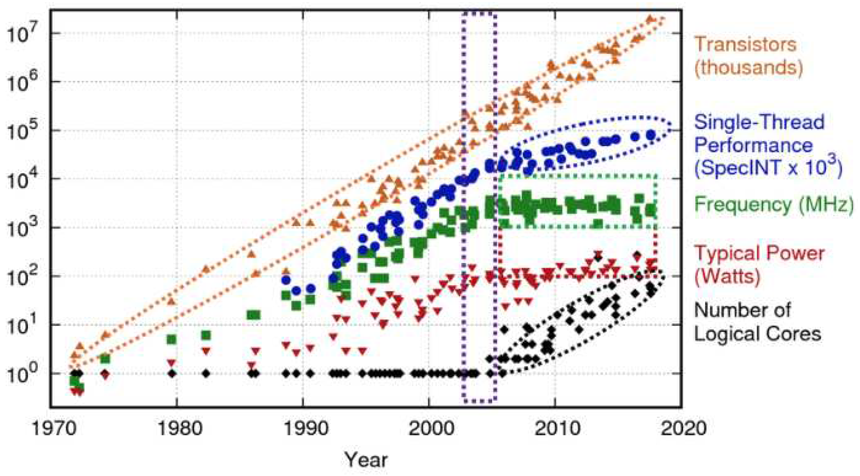
Figure 1. that post 2010 although the transistors are scaling (number of transistors per unit area), the operating frequency, power consumption and even the single threaded performance improvements have flattened or are growing at a much slower pace. This means that the generational leaps of performance and efficiency that we have experienced in the 2000s are no longer possible. Moreover this scaling not only applies for the processor but for other components like DRAM[
3] as well. So the amount of information that we can store per unit area is also decreasing making us unable to design devices that can handle high amounts of data in a small footprint. This motivates the need for us to look for new methods that enable us to achieve performance scaling.
To achieve further scaling in performance we need to use alternate methods to achieve the performance gains. This motivates the need for us to develop new architectures, design methodologies, manufacturing technologies etc. A lot of work is being done in both industry and academia in order to tackle this problem. Various new architectures have been developed each for a specific application. For instance, there have been processors like ARM cortex-M series[
4] targeted towards general purpose low power and low area applications. With the AI boom there has also been a huge number of development in chips that have been specifically optimized for ML calculations[
5], especially matrix multiplications as well as devices for edge AI[
6]. There has also been a huge boom in nano-electronics[
7] and 2-D semiconductors[
8,
9]. There has also been work done on cramming more components within the same resource[
10]. All these are various attempts that have been made in order to tackle future computing requirements.
In the past literature reviews have covered the end of Moore’s Law and its alternate computing methods but there has been no focus on products used in industry. In this paper we will focus on the most popular methods that are currently being developed with a focus on their use in Industry. In this paper we discuss 3 popular methods that are used to achieve high performance after the transistor scaling has ended. These are Large Scale Silicon Die, Chiplets and Quantum Hardware. We will have a brief introduction to what these design methodologies are and their benefits. Which is followed by a look into the most advanced and commercially used product/technology available in each of these design methodologies. Further we will be discussing the pros and cons of each method.
2. Large Scale Silicon die
Traditional Moore’s law is scaling up of performance by increasing the number of transistors. Moving along the same line of thought, apart from scaling transistors per unit area increasing the area of the silicon die i.e making the Monolithic die bigger which in effect leads to more transistors overall seems to be the most logical next step in silicon scaling. Large Scale silicon die’s allow us to pack more components into one single chip offering us higher performance levels. This offers numerous advantages like lower power consumption, higher performance, improved scalability etc. Large scale silicon die’s are primarily focused for AI applications and HPC uses due to their high computational capacities. Furthermore, due to the fact that it has a large area, it does not make it suitable for application with high area constraints.
In this section the focus will be on Cerebras Systems Wafer Scale Engine (WSE) [
11,
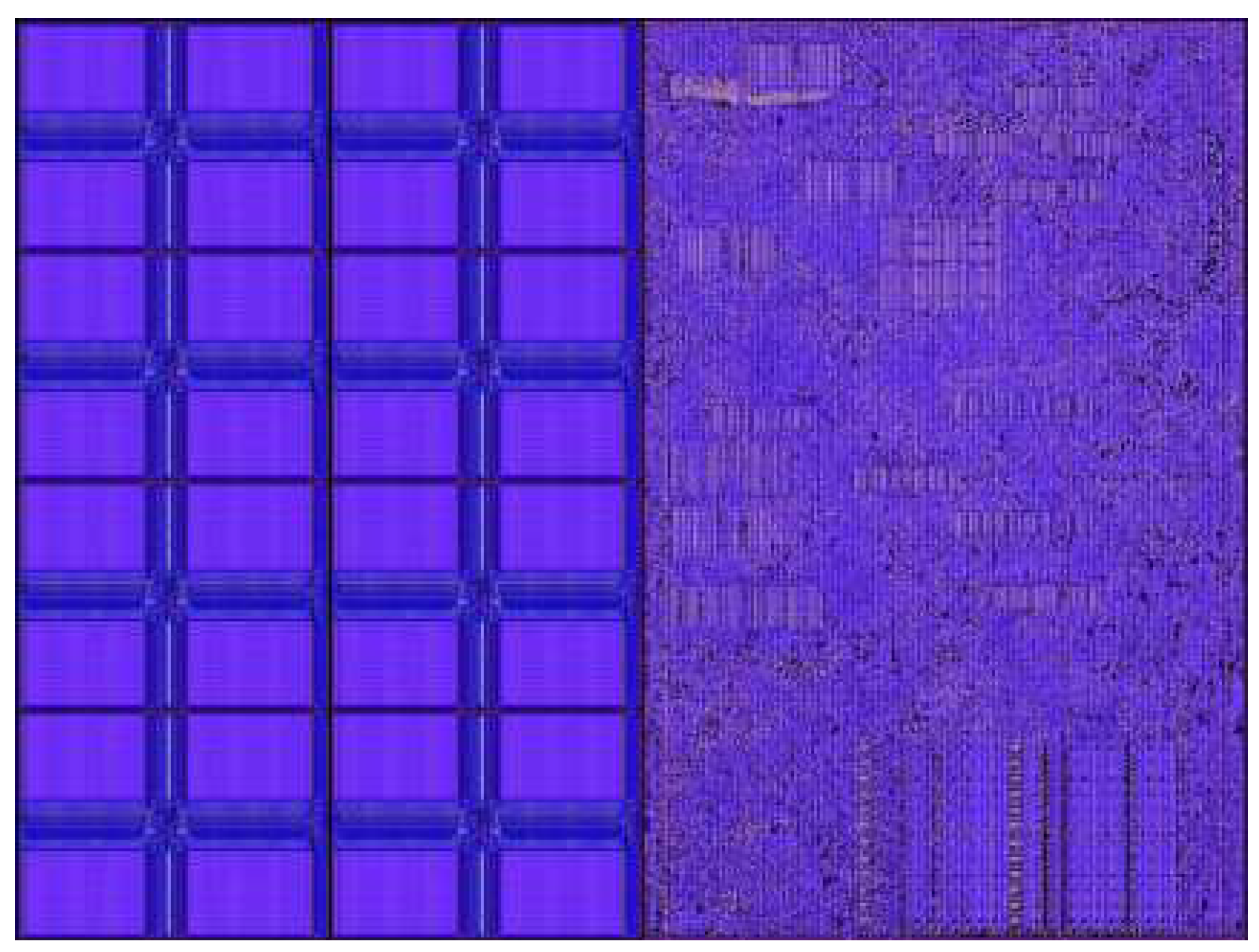
12] as it is the most advanced large scale silicon die currently made. This is a system where the processor itself if of the size of a wafer and is primarily made for ML models and computations. The first iteration was released in 2019 and the second iteration (WSE-2) was released in 2021. The processor produced from WSE-2 has an area 0f 46000mm2, contains 2.6 trillion transistors and has 850000 cores on it. It also uses only SRAM (occupying 50% of the die area as shown
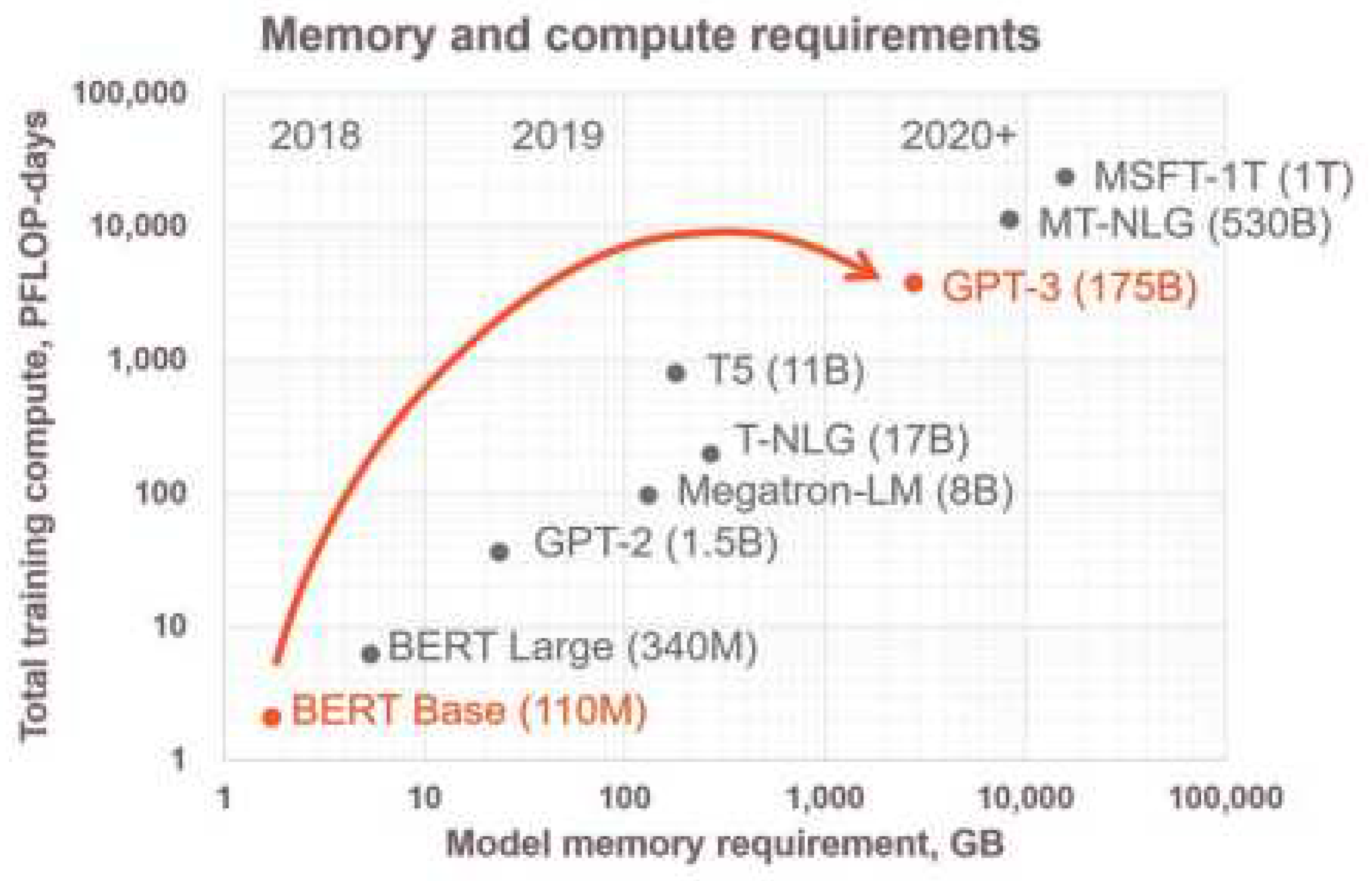
Figure 2) and no DRAM so as to provide full data flow for every single core in the processor. Furthermore, the system uses fine grained data flow accelerators which is extremely useful for sparsity calculations. Combining the factors of high speed memory access along with the increased data flow acceleration, the WSE-2 system is particularly suited for neural networks and ML workloads whose memory requirements have grown exponentially as seen in
Figure 3 which shows the memory requirements of various state-of-the-art neural networks.
An interesting observation to be made in the Cerebras WSE-2 engine is that they only use SRAM and no DRAM. So why is there a need to use only SRAM instead of DRAM? Typical modern processors have a shared central DRAM and often times a shared SRAM cache as well. However, the DRAM access is slow due to its limited bandwidth and is far lower than core data path bandwidth. In a traditional way avoiding this bottleneck is done using caches. In the Cerebras WSE-2 engine by using only SRAM it provides full memory bandwidth to all data paths. The memory is entirely distributed nearby the point of usage in order to do this, enabling memory bandwidth equivalent to the operand bandwidth of the main data channel. This is achieved by making the distance of communication between cores and memory as small as possible. It’s crucial to remember that each core addresses the memory individually. No shared memory in the conventional sense exists. All memory sharing across cores is done explicitly over the fabric to provide genuinely scalable memory. There is a software-managed cache in addition to the high-performance SRAM, which is used for frequently accessed data structures like accumulators. This cache is compact and located very close to the data path in order to reduce power consumption from frequent accesses. Other benefits of using only SRAM instead of DRAM is that we are able to achieve a higher area density of SRAM in the chip as compared to the traditional approach of using caches etc as there is not no need for extra hardware like multi-porting, cache controllers, HBM memory controllers etc. By using such a memory architecture, we are able to run the chip at full performance at all BLAS(Basic Linear Algebraic Subroutines) levels. Whereas in a traditional chip we are limited to running only GEMM(general matrix-matrix multiply) operations only. This is one of the biggest advantages for machine learning workloads where matrix based computations are used extensively. Furthermore, more than 50% of the silicon die is made of SRAM showing its immense capabilities of storing data.
Some other impressive capabilities of the WSE-2 includes its ability to be used as a single Matrix Multiply unit which can prove to be very useful for ML applications. Another crucial innovation in the WSE-2 is the high-bandwidth and low latency fabric. It enable efficient communication across the wafer reducing latency and increasing the overall performance of the chip. This fabric is especially useful in neural network computation. Furthermore, the cores use fine-grained data flow further increasing on-chip communication quality.
Some other popular wafer scale chip is the Graphcore Colossus GC2 IPU [
13]. This is a large scale chip that is designed for artificial intelligence and offers parallel processing capacities suited for ML workloads. Bitmain BM1397 is another large scale silicon die that is designed and used for crypto currency mining.
Although this solution can be used in several applications, it has several limitations. The first being that while computational power is increased, it cannot be used in applications with huge area constraints. Moreover, designing such a large scale system is very difficult. This is because of the various design constraints, physical factors, complications etc involved in designing all the components in a single die[
14]. Also there is a huge problem in extending this method for 2-D semiconductors[
15].
3. Chiplets/Multi-Chip Module (MCM) technology
This is a method that has been invented in order to increase the flexibility in design, improve manufacturing and scaling of silicon dies. By focusing efforts on making the best possible component that does a specific function and later integrating it seamlessly into a larger system opens up huge possibilities for performance scaling in silicon design.
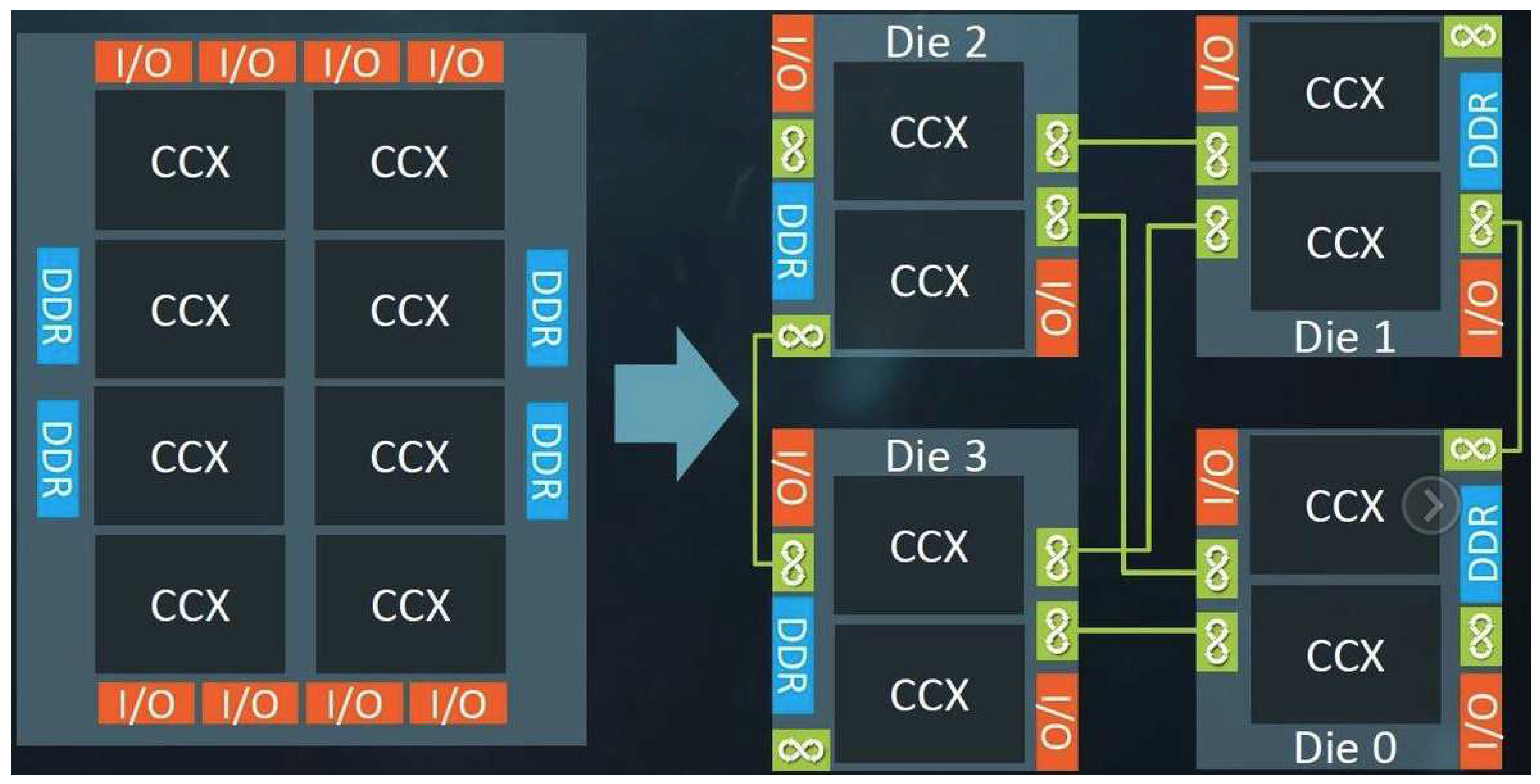
Here multiple individual semiconductor components, or "chiplets," are integrated onto a single package as show in
Figure 4. Each chiplet perform can be a specific function or can be a component like CPU, GPU, I/O controller, memory etc. They offer several benefits[
16,
17]. The most important benefits being modularity where they are able to mix and match individual components to best suit the application. They are also very scalable as you can keep adding and removing chiplets to achieve are desired specification. Furthermore, in this methodology multiple chiplets can be made with manufacturing processes that best suit them and can then later be integrated leading to better chip performance. Moreover, it becomes cheaper to produce small chiplets and then later integrate them into one singe die than massively producing one large die. This is because we are now using less materials and the fact that the turnaround time for multiple chiplets is much faster and can be done in parallel when compared to a Monolithic die. Moreover, the yield is higher when manufacturing a chiplet as compared to a large Monolithic die.
Here we will look into AMDs chiplet design approach. A key component in the chiplet design approach are their interconnects[
18]. The key enablers of AMDs chiplet based design is its infinite fabric[
19]. The infinite fabric is a high speed interconnect which allows for high speed, high bandwidth and low latency communication between different chiplets within the same module. This fabric also allows for Cross-CCX communication between chiplets and CCX clusters. The same is also true for communication between memory controller, CPU and other chiplets. Another important function of the fabric is its ability to allow high speed communication between CPU and GPU allowing for hybrid CPU-GPU architectures. However, the most important benefit of the fabric is that it enables scalability as the latency for large scale server applications are now reduced. The architecture that AMD used for this is called the zen architecture. Here various “zen cores” are connected with memory controllers, chiplets, GPU etc in order to form the final chip. The enabler of all of this is the infinite fabric.
The next stage of development is the AMD infinite architecture. This is foundational model that AMD has developed primarily focused on its data centre applications. This technology offers a huge advantage in using specific technology nodes for different components. For instance, 7nm CPU cores can be combined with 14nm IO and memory components as these are more optimised at 14nm. This helps us take advantage of the best and most optimised process node technology for each component. A SoC design that does away with the requirement for several external support chips and the I/O latency’s they cause is made possible by the use of multiple dies and a fast fabric interface. This leads to a wealth of computing resources having helped data center use cases and also providing high performance and increased hardware security. The most notable application of this approach is the EPYC processor family of AMD[
20]. Another example where the chiplet technology is used is in the Apple M-series line of processors where multiple M1 max chips are combined together to produce the M1 Ultra chip.
Here we see that this method addresses the problem of design constraint and flexibility that the large scale silicon dies do not offer. This solution addresses performance scaling by enabling smart design and choosing the best possible sub-component in the whole system. This is best shown However, this system as well has severe area constraints when it comes to designing because to achieve a huge amount of performance we will need to keep adding more and more chiplets which means we will need more area, which arguably can be more area and power hungry that integrating everything into one singe die.
4. Quantum Computing
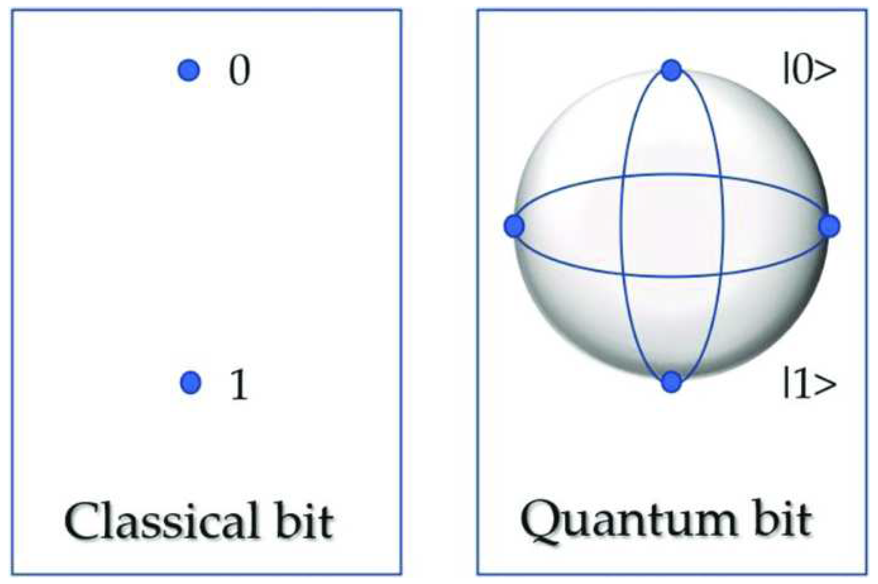
Quantum computers provide a new, unique way of looking into data and processing data. This is a method developed in order to achieve computing capabilities that are impossible with classical computer. The basis of a quantum computer is qubits(quantum bits), which is used instead of bit0/bit1. A qubit can be 0 or 1 simultaneously as shown in
Figure 5. This means we can assign probability to the state of a specific qubit. This enables us to perform calculations on the qubits using its probability, which in turn enables us to compute vast amounts of data. They first superpose all possible computational states and then use the interference circuitry to determine the state of the superposition to give the output. We first look into the 3 most commonly used technologies for quantum computing[
21].
Firstly there is Quantum Annealing. This is the easiest system to build and its computational power is similar to traditional computers. It is mainly used in optimisation problems. The second is Quantum Simulation. This is more powerful that Quantum Annealing and has the power to do more complex computations for chemical and material applications. The last method is Universal Quantum. This is the most powerful but the most difficult system to build. These systems can be used in all types of applications from optimisation to medical to cryptography to fintech[
22].
Compared to the previous 2 methods discussed above quantum computing is not a direct extension of any modern day computing methodology. This technology has the potential to overcome the constraints discussed above i.e it has the potential to achieve the performance requirements we need at the area and power constraints that a lot of application demand. However, developing quantum computers is proving to be a humongous task.
There are several challenges that need to be addressed in order to develop quantum computers. Firstly there are the material issues[
23,
24]. Modern day material are lacking because they often have noise and loss leading to unreliable quantum hardware. The second challenge is to extend the life of the qubits and to prevent decoherence of qubits. The next challenge is to improve scalability of quantum hardware as currently the number of qubits we have is very limited. Moreover, corresponding software stacks should be developed in order to use the computational capabilities of quantum hardware. This should include making it as similar and usable as the software interface of classical computers as only this will this be able to be widely adopted without any problems.
Quantum computing can be used in a wide variety of applications from healthcare in order to analyse chemical and biological compositions to security in cryptography to financial market predictors. A notable application in in cryptography[
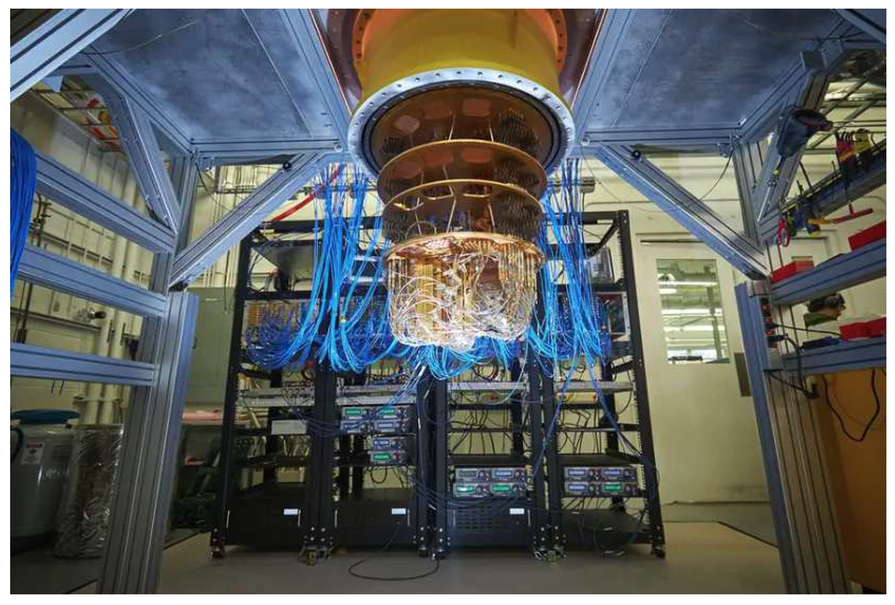
25] where we are able to use quantum computing based random number generators to make better of use of such cryptography based algorithms. The wide variety of applications in quantum computing make it an appealing method in scaling post Moore’s Law. Some companies that work on quantum technology are Google (
Figure 6), IBM (who are working on a 1000 qubit quantum computer[
26]) and D-Wave Systems. D-Wave systems is the 1st company to release a public quantum annealing computer in the market. This technology is still in its early stages and will need to have more time and investment in order to mature.
5. Discussion and Conclusions
In this paper we have explored 3 methods that are used in performance scaling. The first method is the most natural extension of Moore’s Law where we increase the area to increase the number of transistors along with increasing number of transistors per unit area. However, this imposes strict area constraints and it is difficult to design and manufacture. The second method offers us huge flexibility for design and manufacturing, but still does not address the area problem. The last method will solve both the area and performance problems as it is a completely new approach to computing, but since the technology is in its early stages we will have to wait for it to fully develop. These methods summarize the three most common methods used in the industry but they are by no means and exhaustive list.
Some other promising endeavours include analog computing[
27] where we remove the need to take computation into the digital domain and do all computing in analog form (as is true with most signals). This eliminated the need for DACs and other digital only components helping us save in terms of area, power and latency. However, this too has been extremely difficult as designing in analog is magnitudes harder that designing digital systems.
Another popular approach is to use neuromorphic computing[
28] where we try to mimic the computational structure of the human brain i.e our neurons. This also is a promising avenue especially from an energy standpoint as the human brain is one of the most efficient computing mechanisms out of every organism and machine in the world. Other areas for improvement include research on new materials and 2-D semiconductors.
In conclusion, we have explained the need of alternate design approaches that are required for scaling up of computing system in modern times along with popular methods that are being used in industry in order to achieve performance scaling. Although transistor scaling is approaching its end, this does not stop us from thinking of new and innovative architectures and design methodologies to meet our computing needs. To meet the computing needs of the future we will have to keep innovating on how to increase the performance of semiconductors.
References
- Charles E. Leiserson, Neil C. Thompson, Joel S. Emer, Bradley C. Kuszmaul, Butler W. Lampson, Daniel Sanchez, and Tao B. Schardl. There’s plenty of room at the top: What will drive computer performance after moore’s law? Science, 368(6495):eaam9744, 2020.
- Thomas N. Theis and H.-S. Philip Wong. The end of moore’s law: A new beginning for information technology. Computing in Science & Engineering, 19(2):41–50, 2017.
- J.W. Han, S.H. Park, M.Y. Jeong, K.S. Lee, K.N. Kim, H.J. Kim, J.C. Shin, S.M. Park, S.H. Shin, S.W. Park, K.S. Lee, J.H. Lee, S.H. Kim, B.C Kim, M.H. Jung, I.Y. Yoon, H. Kim, S.U. Jang, K.J. Park, Y.K. Kim, I.G. Kim, J.H Oh, S.Y. Han, B.S. Kim, B.J. Kuh, and J.M. Park. Ongoing evolution of dram scaling via third dimension -vertically stacked dram -. In 2023 IEEE Symposium on VLSI Technology and Circuits (VLSI Technology and Circuits), pages 1–2, 2023.
- Hemanthkumar P B, Shreekar Reddy Anireddy, Josh F T, and Venkatesan R. Introduction to arm processors & its types and overview to cortex m series with deep explanation of each of the processors in this family. In 2022 International Conference on Computer Communication and Informatics (ICCCI), pages 1–8, 2022.
- Bingzhen Li, Jiaojiao Gu, and Wenzhi Jiang. Artificial intelligence (ai) chip technology review. In 2019 International Conference on Machine Learning, Big Data and Business Intelligence (MLBDBI), pages 114–117, 2019.
- Tuomo Sipola, Janne Alatalo, Tero Kokkonen, and Mika Rantonen. Artificial intelligence in the iot era: A review of edge ai hardware and software. volume 31, pages 320–331, 04 2022.
- Taha Basheer Taha, Azeez Abdullah Barzinjy, Faiq Hama Seaeed Hussain, and Togzhan Nurtayeva. Nanotechnology and computer science: Trends and advances. Memories - Materials, Devices, Circuits and Systems, 2:100011, 2022.
- Ming-Yang Li, Sheng-Kai Su, H-S Philip Wong, and Lain-Jong Li. How 2d semiconductors could extend moore’s law. Nature, 567(7747):169–170, 2019.
- Yuanyuan Shi Shaochuan Chen, Mohammad Reza Mahmoodi. Wafer-scale integration of two-dimensional materials in high-density memristive crossbar arrays for artificial neural networks. Nature Electronics, 3:638–645, 2020.
- Gordon, E. Gordon E. Moore. Cramming more components onto integrated circuits, reprinted from electronics, volume 38, number 8, april 19, 1965, pp.114 ff. IEEE Solid-State Circuits Society Newsletter, 11(3):33–35, 2006.
- Gary Lauterbach. The path to successful wafer-scale integration: The cerebras story. IEEE Micro, 41(6):52–57, 2021.
- Sean Lie. Cerebras architecture deep dive: First look inside the hardware/software co-design for deep learning. IEEE Micro, 43(3):18–30, 2023.
- Samuel Maddrell-Mander, Lakshan Mohan, Alexander Marshall, Daniel O’Hanlon, Konstantinos Petridis, Jonas Rademacker, Victoria Rege, and Alexander Titterton. Studying the potential of graphcore ipus for applications in particle physics. Computing and Software for Big Science, 5, 12 2021.
- Johann Knechtel, Ozgur Sinanoglu, Ibrahim Abe M Elfadel, Jens Lienig, and Cliff CN Sze. Large-scale 3d chips: Challenges and solutions for design automation, testing, and trustworthy integration. IPSJ Transactions on System LSI Design Methodology, 10:45–62, 2017.
- Tom Schram, Surajit Sutar, Iuliana Radu, and Inge Asselberghs. Challenges of wafer-scale integration of 2d semiconductors for high-performance transistor circuits. Advanced Materials, 34(48):2109796, 2022.
- Tao Li, Jie Hou, Jinli Yan, Rulin Liu, Hui Yang, and Zhigang Sun. Chiplet heterogeneous integration technology—status and challenges. Electronics, 9(4), 2020.
- Gabriel H. Loh, Samuel Naffziger, and Kevin Lepak. Understanding chiplets today to anticipate future integration opportunities and limits. In 2021 Design, Automation & Test in Europe Conference & Exhibition (DATE), pages 142–145, 2021.
- Yinxiao Feng, Dong Xiang, and Kaisheng Ma. A scalable methodology for designing efficient interconnection network of chiplets. In 2023 IEEE International Symposium on High-Performance Computer Architecture (HPCA), pages 1059–1071, 2023.
- FromAMD. Amd infinte fabric, 2019.
- Samuel Naffziger, Noah Beck, Thomas Burd, Kevin Lepak, Gabriel H. Loh, Mahesh Subramony, and Sean White. Pioneering chiplet technology and design for the amd epyc™ and ryzen™ processor families : Industrial product. In 2021 ACM/IEEE 48th Annual International Symposium on Computer Architecture (ISCA), pages 57–70, 2021.
- Arthi Udayakumar. Quantum computing — the next gen, 2019.
- Narcisa Roxana Mosteanu and Alessio Faccia. Fintech frontiers in quantum computing, fractals, and blockchain distributed ledger: Paradigm shifts and open innovation. Journal of Open Innovation: Technology, Market, and Complexity, 7:19, 01 2021.
- James N Eckstein and Jeremy Levy. Materials issues for quantum computation. MRS Bulletin, 38(10):783–789, 2013.
- Matt Swayne. What are the remaining challenges of quantum computing?, 2023.
- Mario Stipcevic. Quantum random number generators and their applications in cryptography. In Advanced photon counting techniques VI, volume 8375, pages 20–34. SPIE, 2012.
- Adrian Cho. Ibm promises 1000-qubit quantum computer—a milestone—by 2023. Science, 15, 2020.
- Sven Köppel, Bernd Ulmann, Lars Heimann, and Dirk Killat. Using analog computers in today’s largest computational challenges. Advances in Radio Science, 19:105–116, December 2021.
- Hitesh Vora, Preeti Kathiria, Smita Agrawal, and Usha Patel. Neuromorphic computing: review of architecture, issues, applications and research opportunities. Recent Innovations in Computing: Proceedings of ICRIC 2021, Volume 2, pages 371–383, 2022.
- P.K. Chaturvedi. Wafer scale integration: a review. Microelectronics Journal, 19(2):4–35, 1988.
- Russel Aubusson. Wafer-scale integration of semiconductor memory. PhD thesis, Middlesex Polytechnic, 2011.
- Antonio D. Córcoles, Abhinav Kandala, Ali Javadi-Abhari, Douglas T. McClure, Andrew W. Cross, Kristan Temme, Paul D. Nation, Matthias Steffen, and Jay M. Gambetta. Challenges and opportunities of near-term quantum computing systems. Proceedings of the IEEE, 108(8):1338–1352, 2020.
- Jacob Devlin, Ming-Wei Chang, Kenton Lee, and Kristina Toutanova. Bert: Pre-training of deep bidirectional transformers for language understanding, 2019.
- Yufei Ding and Ali Javadi-Abhari. Quantum and post-moore’s law computing. IEEE Internet Computing, 26(1):5–6, 2022.
- Artur Ekert, PM Hayden, and Hitoshi Inamori. Basic concepts in quantum computation. In Coherent atomic matter waves: 27 July–27 August 1999, pages 661–701. Springer, 2001.
- Li Gao. Flexible device applications of 2d semiconductors. Small, 13(35):1603994, 2017.
- Laurentiu-Mihai Ionescu, Alin Mazare, Constantin Anton, and Catalin Stoian. The hardware implementation of a quantum computation system emulator. In 2014 International Conference on Applied Electronics, pages 121–124, 2014.
- JEDEC. High bandwidth memory (hbm3) dram,, 2023.
- Kuldeep Singh Kaswan, Jagjit Singh Dhatterwal, Anupam Baliyan, and Shalli Rani. Introduction of Quantum Computing, pages 1–32. 2023.
- Sean Lie. Multi-million core, multi-wafer ai cluster. In 2021 IEEE Hot Chips 33 Symposium (HCS), pages 1–41, 2021.
- Di Lu, Tzu-Li Liu, Jan-Kai Chang, Dongsheng Peng, Yi Zhang, Jiho Shin, Tao Hang, Wubin Bai, Quansan Yang, and John A Rogers. Transient light-emitting diodes constructed from semiconductors and transparent conductors that biodegrade under physiological conditions. Advanced Materials, 31(42):1902739, 2019.
- Joe Macri. Amd’s next generation gpu and high bandwidth memory architecture: Fury. In 2015 IEEE Hot Chips 27 Symposium (HCS), pages 1–26, 2015.
- Rangan Majumder. Deepspeed: Extreme-scale model training for everyone, 2020.
- Samuel Naffziger, Kevin Lepak, Milam Paraschou, and Mahesh Subramony. 2.2 amd chiplet architecture for high-performance server and desktop products. In 2020 IEEE International Solid-State Circuits Conference - (ISSCC), pages 44–45, 2020.
- Moinuddin Qureshi and Swamit Tannu. Quantum computing and the design of the ultimate accelerator. IEEE Micro, 41(5):8–14, 2021.
- Johannes Schemmel, Johannes Fieres, and Karlheinz Meier. Wafer-scale integration of analog neural networks. In 2008 IEEE International Joint Conference on Neural Networks (IEEE World Congress on Computational Intelligence), pages 431–438, 2008.
- Jueli Shi, Jiaye Zhang, Lu Yang, Mei Qu, Dong-Chen Qi, and Kelvin HL Zhang. Wide bandgap oxide semiconductors: from materials physics to optoelectronic devices. Advanced materials, 33(50):2006230, 202.
- Melanie Swan, Renato Dos Santos, and Frank Witte. Quantum information science. IEEE Internet Computing, PP:1–1, 12 2021.
- Benjamin Villalonga, Dmitry Lyakh, Sergio Boixo, Hartmut Neven, Travis S Humble, Rupak Biswas, Eleanor G Rieffel, Alan Ho, and Salvatore Mandrà. Establishing the quantum supremacy frontier with a 281 pflop/s simulation. Quantum Science and Technology, 5(3):034003, 2020.
- Yang Xue. Recent development in analog computation: a brief overview. Analog Integrated Circuits and Signal Processing, 86:181–187, 2016.
- Zheqi Yu, Amir M. Abdulghani, Adnan Zahid, Hadi Heidari, Muhammad Ali Imran, and Qammer H. Abbasi. An overview of neuromorphic computing for artificial intelligence enabled hardware-based hopfield neural network. IEEE Access, 8:67085–67099, 2020.
- Florian Zaruba, Fabian Schuiki, and Luca Benini. Manticore: A 4096-core risc-v chiplet architecture for ultraefficient floating-point computing. IEEE Micro, 2021; 42, 36–42.
- Hao Zheng, Ke Wang, and Ahmed Louri. A versatile and flexible chiplet-based system design for heterogeneous manycore architectures. In 2020 57th ACM/IEEE Design Automation Conference (DAC), pages 1–6, 2020.
|
Disclaimer/Publisher’s Note: The statements, opinions and data contained in all publications are solely those of the individual author(s) and contributor(s) and not of MDPI and/or the editor(s). MDPI and/or the editor(s) disclaim responsibility for any injury to people or property resulting from any ideas, methods, instructions or products referred to in the content. |
© 2023 by the authors. Licensee MDPI, Basel, Switzerland. This article is an open access article distributed under the terms and conditions of the Creative Commons Attribution (CC BY) license (http://creativecommons.org/licenses/by/4.0/).
