Submitted:
04 December 2023
Posted:
04 December 2023
You are already at the latest version
Abstract
Keywords:
1. Introduction
2. Proposed Twin Frequency Control DC-DC Buck Converter
 (1)
(1)
 (2)
(2)
 (3)
(3)
1.1. Proposed Accurate Load Current Sensing (ALCS) Block
 (4)
(4)
 (5)
(5)
 (6)
(6)
 (7)
(7)
 (8)
(8)
 (9)
(9)
 (10)
(10)
 (11)
(11)
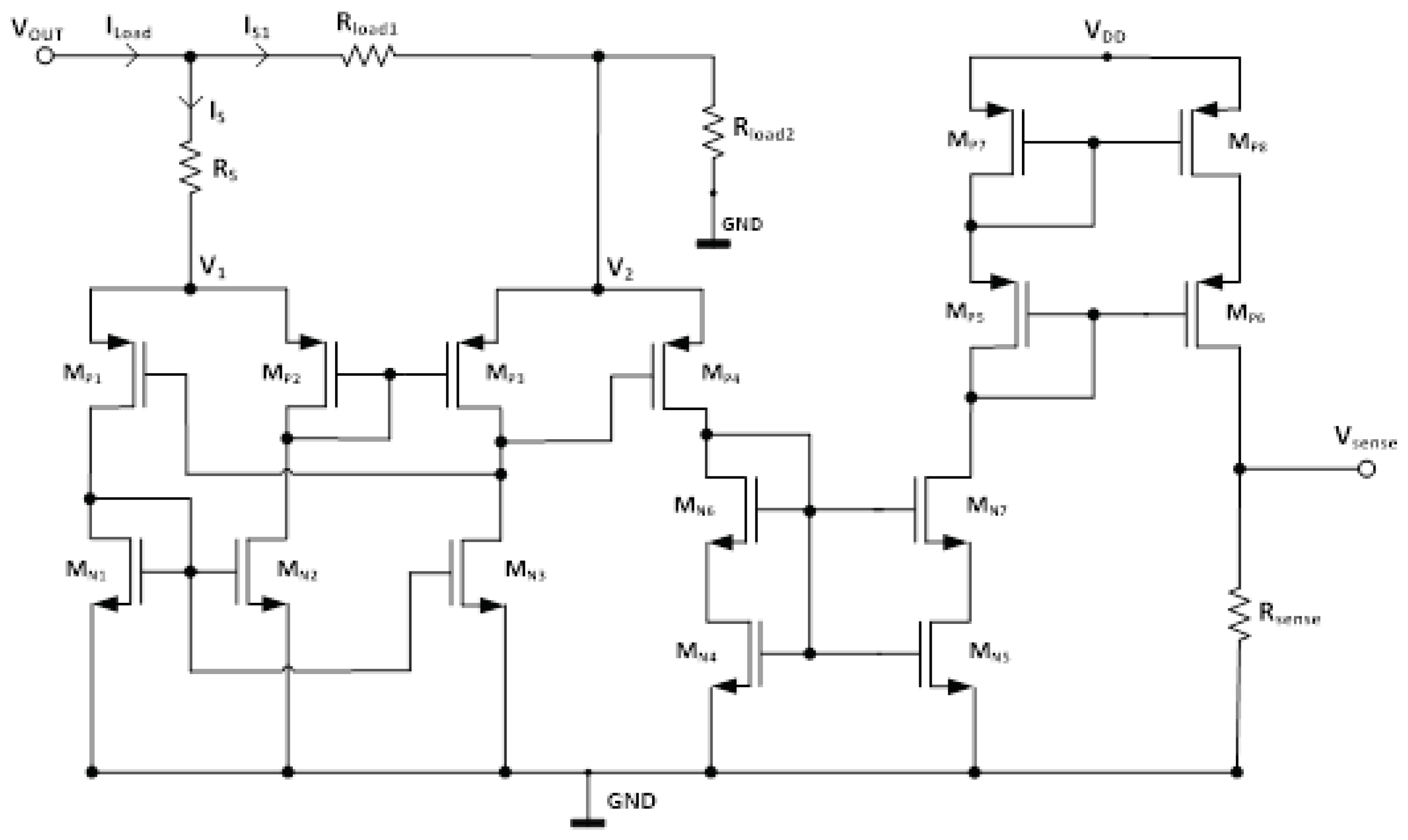
 (12)
(12)
 (13)
(13)
 (14)
(14)
 is a constant.
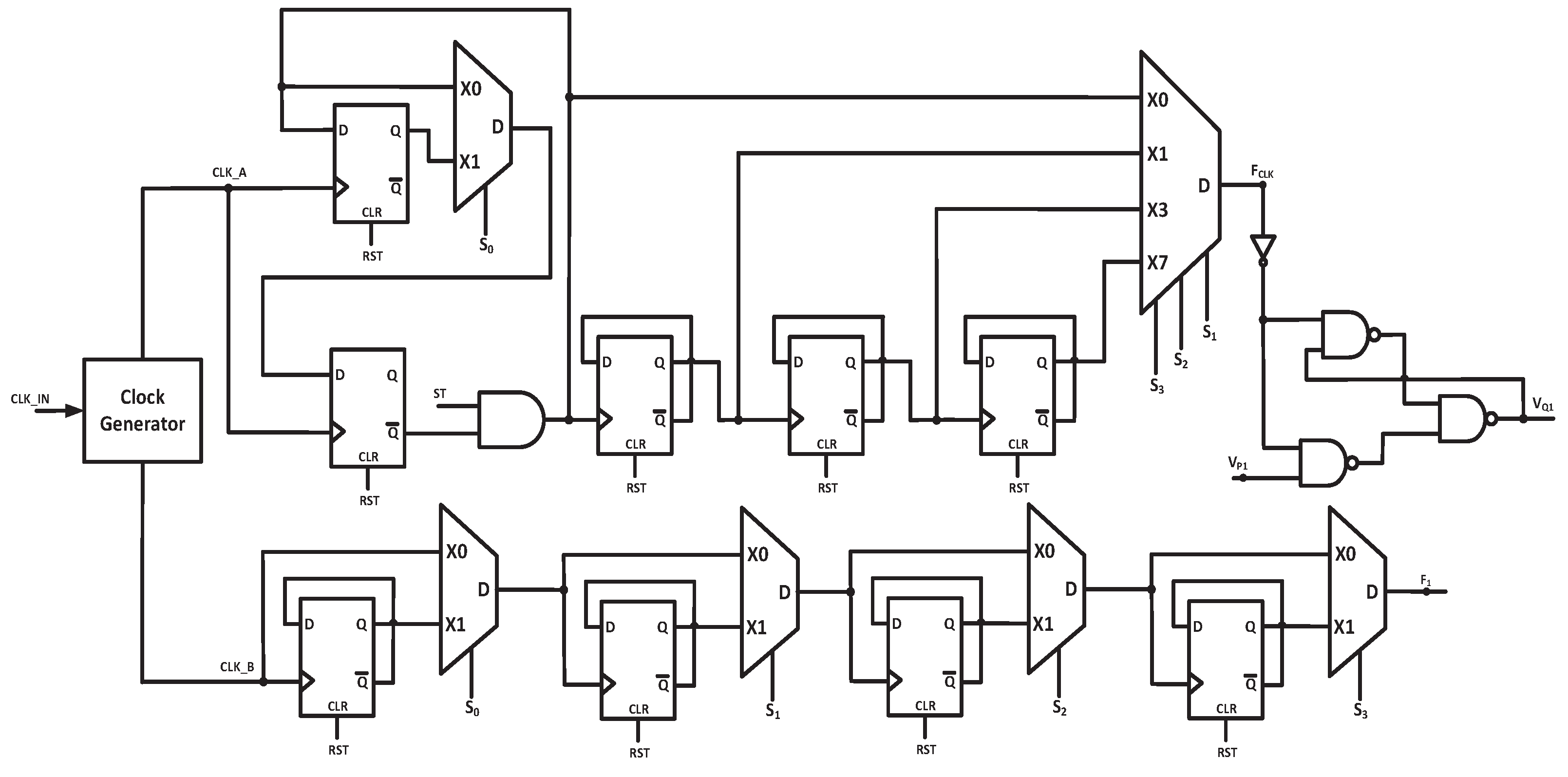
1.3. Proposed Twin Frequency Control Scheme (TFCS)
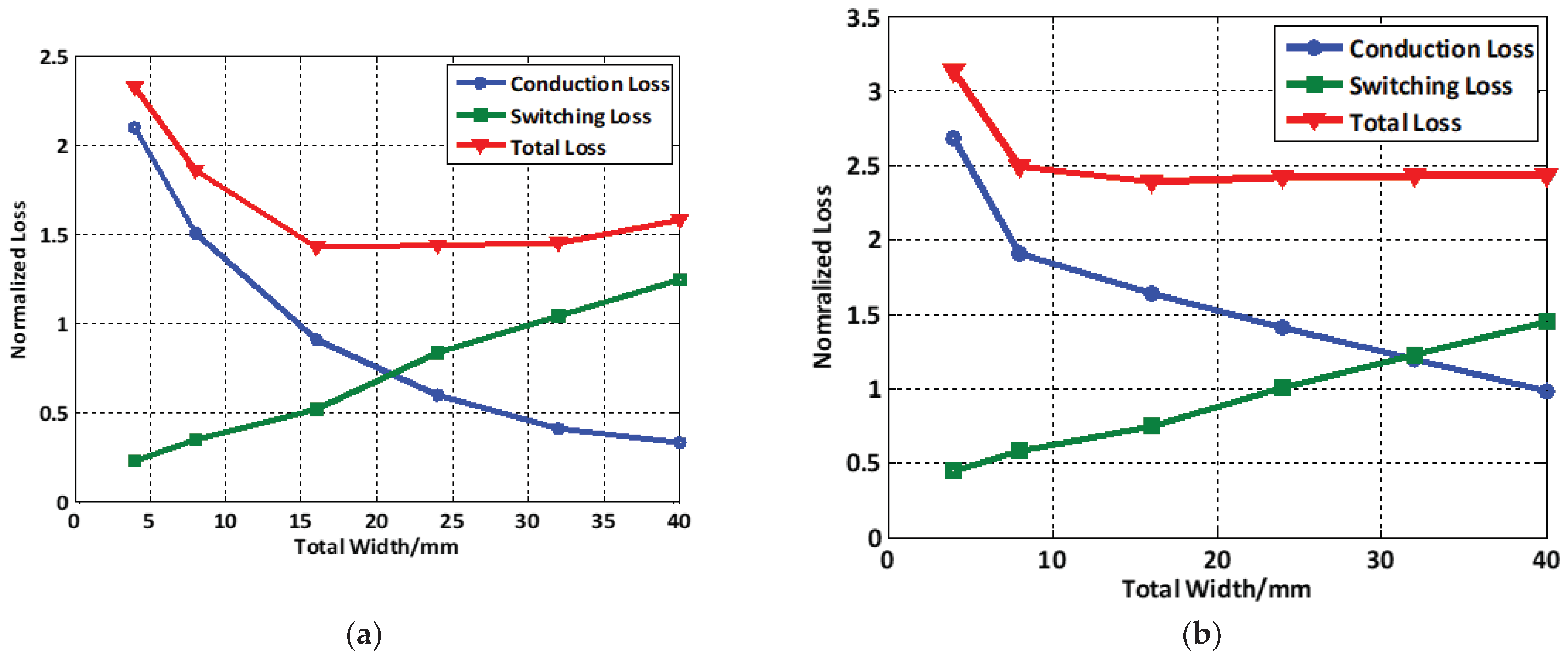
1.4. Power Train
 (15)
(15)
 (16)
(16)
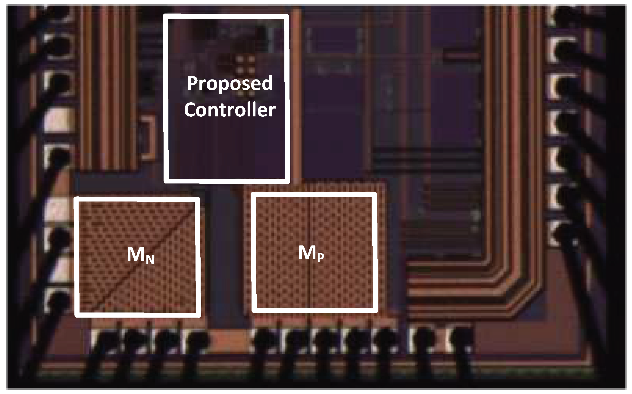
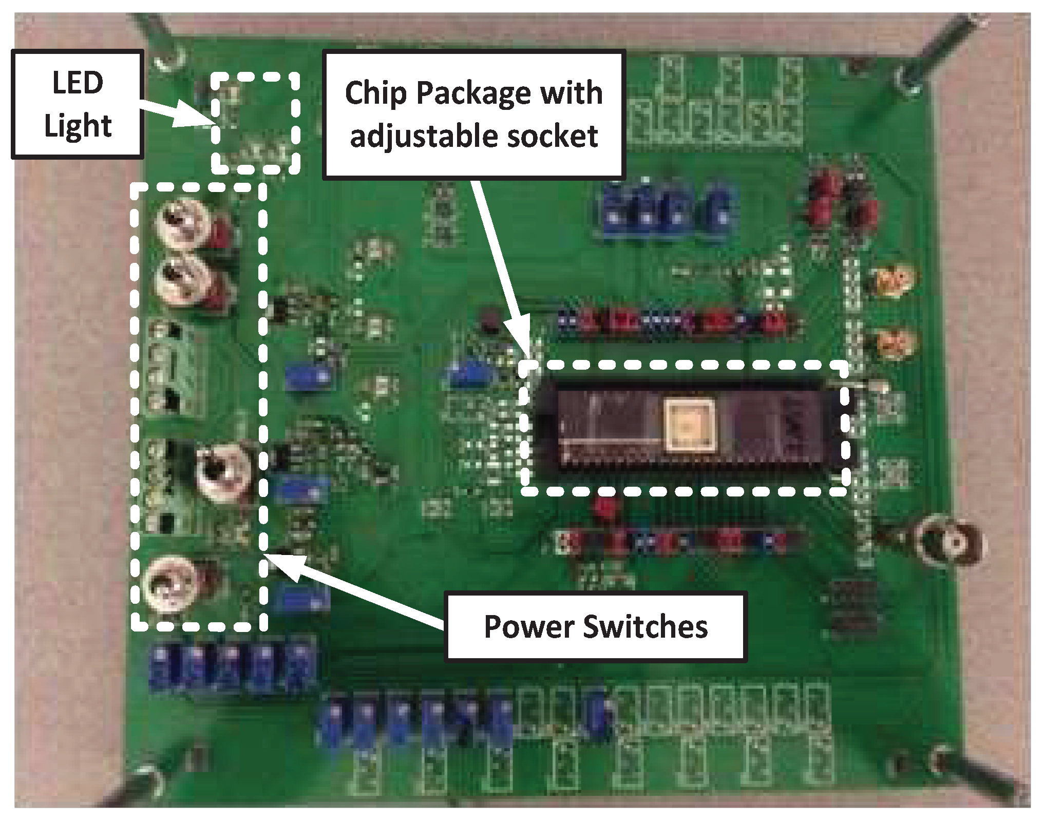
3. Experimental Results
4. Conclusions
Acknowledgments
6. Appendix
References
- W. J. Lee, Y. Z. Wang, D. H. Shin, N. H. Chang, and M. Pedram, "Power conversion efficiency characterization and optimization for smartphones," in Int. Symp. on Low Power Electronics and Design, 2012, pp. 103–108.
- A. Carrol and G. Heiser, "An Analysis of Power Consumption in a Smartphone," Proc. of the USENIX Annual Technical Conference, pp. 271–284, June 2010.
- Y. Huh, "Future direction of power management in mobile devices," in Proc. IEEE Asian Solid State Circuits Conf. (ASSCC), 2011, pp. 1–4.
- H. Kim, "Trends of R&D on Lithium Secondary Batteries for Electricial Vehicles," Smart Battery/Cell Forum, June 2011, Seoul, Korea.
- M. Dong and L. Zhong, "Self-constructive high-rate system energy modeling for battery-powered mobile systems," in 9th Int. Conf. on Mobile Systems, 2011, pp. 335–348.
- Z. Lide, B. Tiwana, R. P. Dick, Q. Zhiyun, Z. M. Mao, W. Zhaoguang, and Y. Lei, "Accurate online power estimation and automatic battery behavior based power model generation for smartphones," in IEEE Int. Conference on Hardware/Software Codesign and System Synthesis, 2010, pp. 105–14.
- D. Ma and R. Bondade, "Enabling Power-Efficient DVFS Operations on Silicon," IEEE Circuits Syst. Mag., vol. 10, pp. 14–30, 2010. [CrossRef]
- S. Chester, "Characteristics of Rechargeable Batteries," Texas Instruments Appl. Rep. no. "SNVA533", 2011.
- B. Sahu and G. A. Rincon-Mora, "A high-efficiency, dual-mode, dynamic, buck-boost power supply IC for portable applications," in 18th Int. Conf. on VLSI Design, 2005, pp. 858–861.
- T. Instruments. Handset: Smartphone [Online]. Available: http://www.ti.com/solution/handset_smartphone.
- B. Sahu and G. A. Rincon-Mora, "An Accurate, Low-Voltage, CMOS Switching Power Supply With Adaptive On-Time Pulse-Frequency Modulation (PFM) Control," IEEE Trans. Circuits Syst. I, vol. 54, pp. 312–321, 2007. [CrossRef]
- M. D. Mulligan, B. Broach, and T. H. Lee, "A constant-frequency method for improving light-load efficiency in synchronous buck converters," IEEE Trans. Power Electron Lett., vol. 3, pp. 24–29, 2005. [CrossRef]
- H. Lee and S.-R. Ryu, "An Efficiency-Enhanced DCM Buck Regulator With Improved Switching Timing of Power Transistors," IEEE Trans. Circuits Syst. II, Exp. Briefs, vol. 57, pp. 238–242, Mar. 2010. [CrossRef]
- Z. C. Sun and L. Siek, "A novel ripple controlled modulation for high efficiency DC-DC converters," in 13th Int. Symp. on Integrated Circuits (ISIC), 2011, pp. 238–241.
- S. Musunuri and P. L. Chapman, "Improvement of light-load efficiency using width-switching scheme for CMOS transistors," IEEE Trans. Power Electron Lett., vol. 3, pp. 105–110, 2005. [CrossRef]
- H.-W. Huang, K.-H. Chen, and S.-Y. Kuo, "Dithering Skip Modulation, Width and Dead Time Controllers in Highly Efficient DC-DC Converters for System-On-Chip Applications," IEEE J. Solid-State Circuits, vol. 42, pp. 2451–2465, 2007. [CrossRef]
- Y. H. Lam, W. H. Ki, C. Y. Tsui, and D. Ma, "Integrated 0.9 V charge-control switching converter with self-biased current sensor," in IEEE Int'l Midwest Symp. on Ckts. & Sys., pp. 305–308, Jul. 2004.
- A. J. Stratakos, S. R. Sanders, and R. W. Brodersen, "A low-voltage CMOS DC-DC converter for a portable battery-operated system," in Proc. IEEE Power Electron. Specialist Conf., Jun. 1994, pp. 619–626.
- Y. Katayama, M. Edo, T. Denta, T. Kawashima, and T. Ninomiya, "Optimum design method of CMOS IC for DC-DC converter that integrates power stage MOSFETs," in Proc. IEEE Power Electron. Specialist Conf., 2004, pp. 4486–4491.
- Y. Chen, Y. Fu, X. Cheng, T. X. Wu, and Z. J. Shen, "Modeling and Analysis of Metal Interconnect Resistance of Power IC's," in Proc. IEEE Int. Symp. Power Semiconductor Devices and IC's, 2007, pp. 253–256.
- L. Baker, R. Currences, S. Law, M. Le, C. Lee, S. T. Lin, and M. Teene, "A `waffle' layout technique strengthens the ESD hardness of the NMOS output transistor," in Proc. Symp. on Electrical Overstress/Electrostatic Discharge, 1989, pp. 175–81.
- A. V. d. Bosch, M. S. J. Steyaert, and W. Sansen, "A high density matched hexagonal transistor structure in standard CMOS technology for high speed applications," in Proc. IEEE Int. Conf. Microelectronic Test Structures, 1999, pp. 212–215.
- A. Yoo, M. Chang, O. Trescases, and W. T. Ng, "High Performance Low-Voltage Power MOSFETs with Hybrid Waffle Layout Structure in a 0.25µm Standard CMOS Process," in Proc. IEEE Int. Symp. Power Semiconductor Devices and IC's, 2008, pp. 95–98.
- A. Yoo, "Design, Implementation, Modeling, and Optimization of Next Generation Low-Voltage Power MOSFETs," Ph.D. dissertation, Department of Materials Science and Engineering, University of Toronto, Canada, 2010.
- Z. C. Sun, K. W. R. Chew, H. Tang, and L. Siek, "Adaptive Gate Switching Control for Discontinuous Conduction Mode DC-DC Converter," IEEE Trans. Power Electron., vol. 29, no. 3, pp. 1311–1320, March 2014. [CrossRef]
- T.-H. Kong, Y.-J. Woo, S.-W. Wang, S.-W. Hong, and G.-H. Cho, "Zero-order control of boost DC-DC converter with transient enhancement using residual current " in IEEE ISSCC Dig. Tech. Papers, 2011, pp. 390–392.
- T. Y. Man, P. K. T. Mok, and M. J. Chan, "A 0.9-V Input Discontinuous-Conduction-Mode Boost Converter With CMOS-Control Rectifier," IEEE J. Solid-State Circuits, vol. 43, no. 9, pp. 2036–2046, Sept. 2008. [CrossRef]
- W. Yan, W. Li, and R. Liu, "A Noise-Shaped Buck DC-DC Converter With Improved Light-Load Efficiency and Fast Transient Response," IEEE Trans. Power Electron., vol. 26, no. 12, pp. 3908–3924, Dec. 2011. [CrossRef]
- O. Trescases, G. Wei, A. Prodic, and W. T. Ng, "Predictive Efficiency Optimization for DC-DC Converters With Highly Dynamic Digital Loads," IEEE Trans. Power Electron., vol. 23, pp. 1859–1869, Jul. 2008. [CrossRef]
- K. Wong, "Parasitics can Hinder Switching Regulator and LDO Designs," Texas Instruments Appl. Rep. no. "SNVA689", May. 2013.
- T. A. Smith, S. Dimitrijev, and H. B. Harrison, "Controlling a DC-DC converter by using the power MOSFET as a voltage controlled resistor," IEEE Trans. Circuits and Syst. I, vol. 47, no. 3, pp. 357–362, Mar. 2000. [CrossRef]
- H. P. Forghani-Zadeh and G. A. Rincon-Mora, "An Accurate, Continuous, and Lossless Self-Learning CMOS Current-Sensing Scheme for Inductor-Based DC-DC Converters," IEEE J. Solid-State Circuits, vol. 42, no. 3, pp. 665–679, Mar. 2007. [CrossRef]
- C. Y. Leung, P. K. T. Mok, K. N. Leung, and M. Chan, "An integrated CMOS current-sensing circuit for low-Voltage current-mode buck regulator," IEEE Trans. Circuits Syst. II, vol. 52, no. 7, pp. 394–397, Jul. 2005. [CrossRef]
- C. Y. Leung, P. K. T. Mok, and K. N. Leung, "A 1-V integrated current-mode boost converter in standard 3.3/5-V CMOS technologies," IEEE J. Solid-State Circuits, vol. 40, no. 11, pp. 2265–2274, Nov. 2005. [CrossRef]
- C. F. Lee and P. K. T. Mok, "A monolithic current-mode CMOS DC-DC converter with on-chip current-sensing technique," IEEE J. Solid-State Circuits, vol. 39, no. 1, pp. 3–14, Jan. 2004. [CrossRef]
- P. Drennan and C. McAndrew, "Understanding MOSFET mismatch for analog design," IEEE J. Solid-State Circuits, vol. 38, no. 3, pp. 450–456, Mar. 2003. [CrossRef]
- H. Y. H. Lam, W. H. Ki, and D. Ma, "Loop gain analysis and development of high-speed high-accuracy current sensors for switching converters," in Proc. IEEE Int. Symp. Circuits and Syst. May 2004, pp. 828–831.
- M. Corsi, "Current sensing schemes for use in BiCMOS integrated circuits," in Proc. IEEE Bipolar/BiCMOS Circuits and Technology Meeting, Oct. 1995, pp. 55–57.
- E. Dallago, M. Passoni, and G. Sassone, "Lossless current sensing in low-voltage high-current DC/DC modular supplies," IEEE Trans. Ind. Electron. vol. 47, pp. 1249–1252, Dec 2000. [CrossRef]
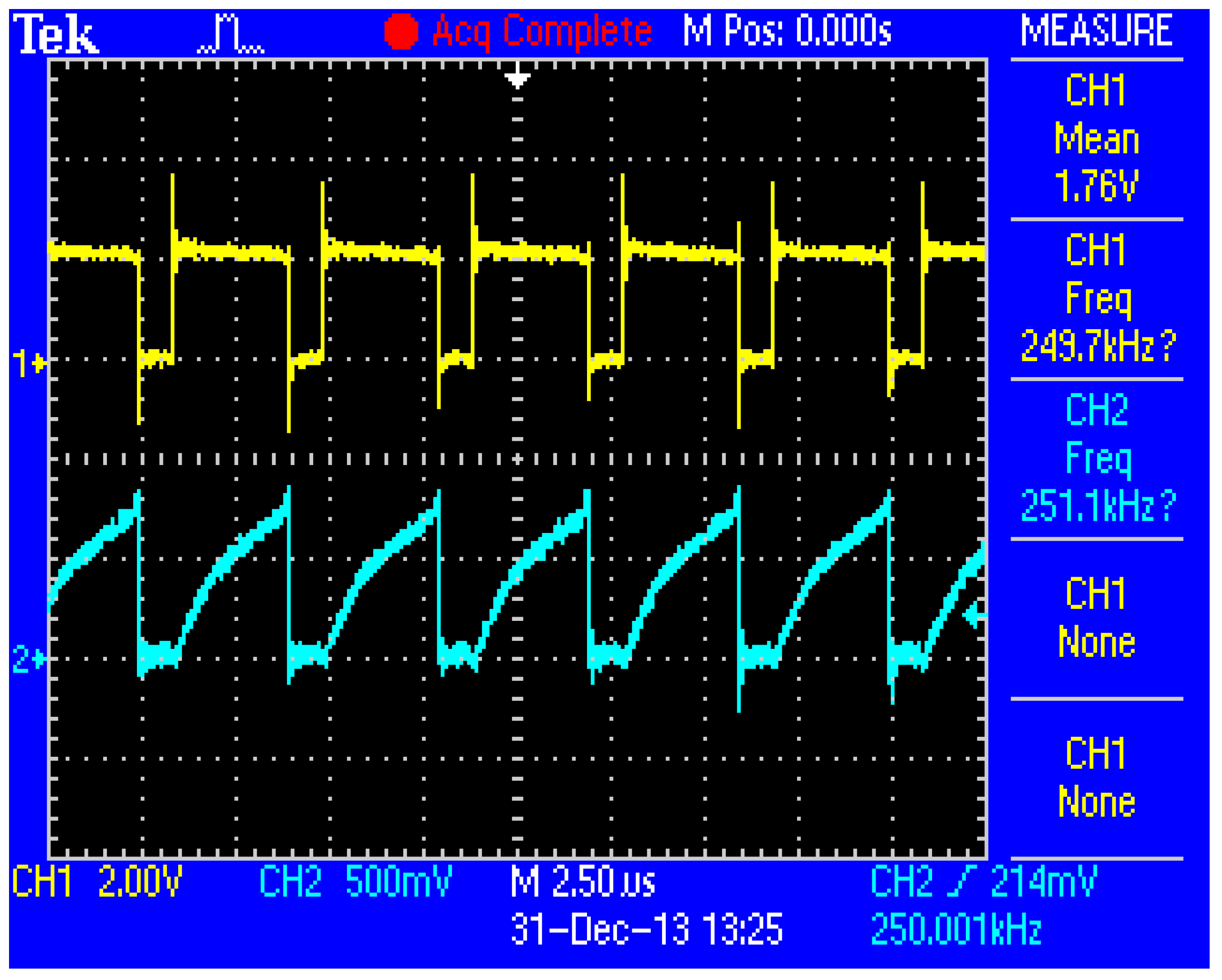
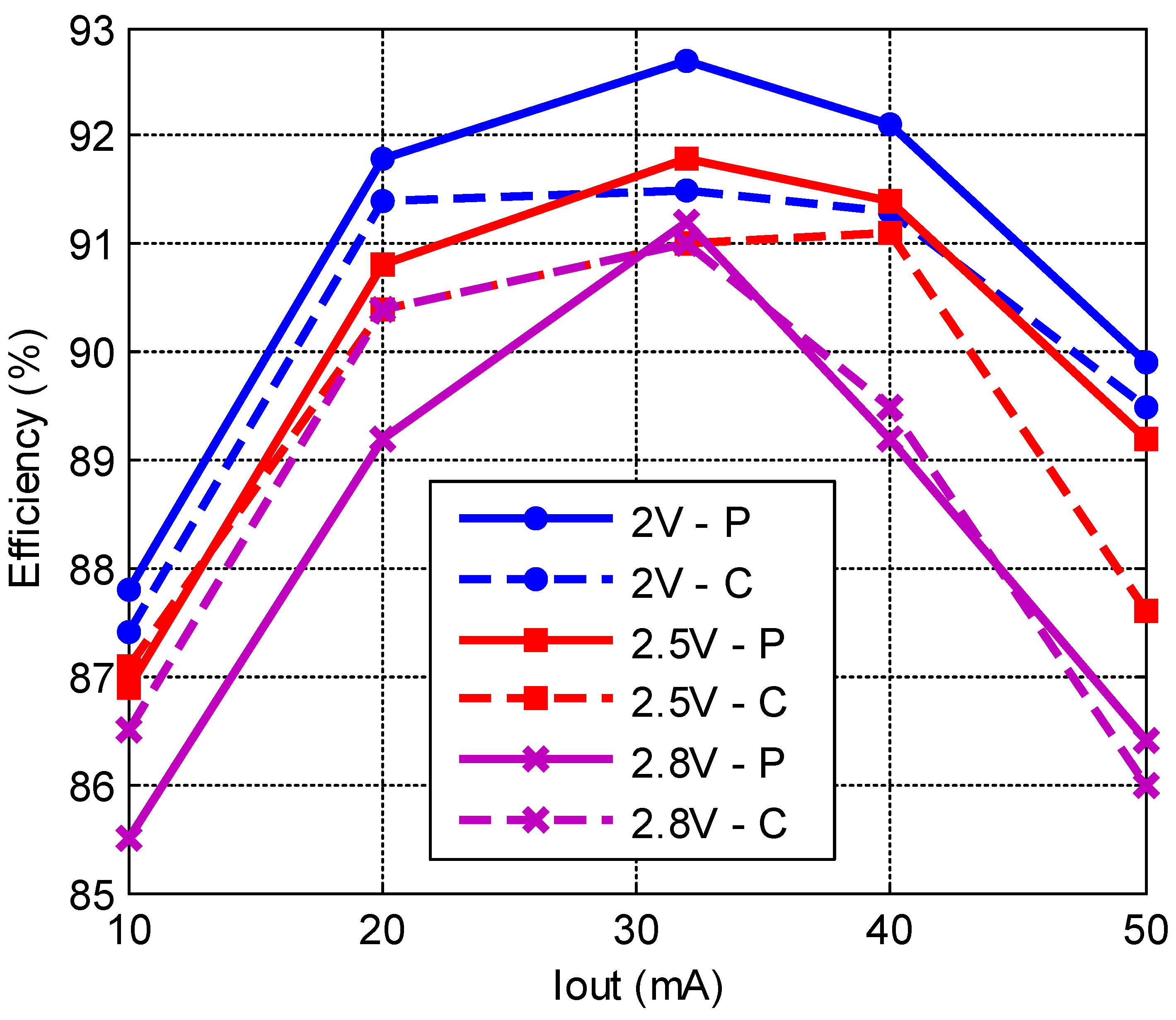
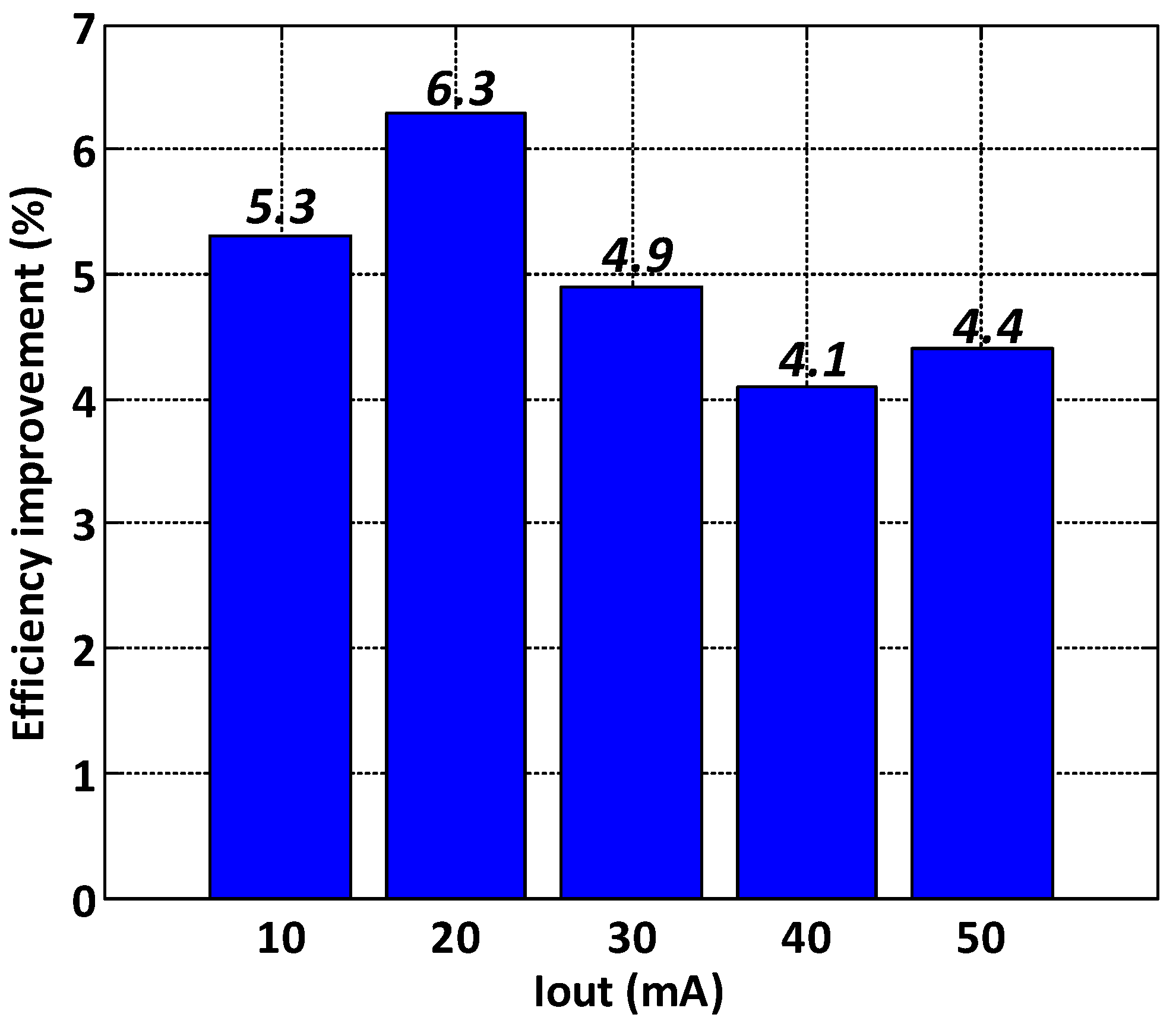
| Units | JSSC [27] | TPEL [28] | TPEL [25] | This Work | ||||||
|---|---|---|---|---|---|---|---|---|---|---|
| Year | - | 2008 | 2011 | 2013 | 2013 | |||||
| Technology | µm | 0.35 | 0.35 | 0.18 | 0.18 | |||||
| Input Voltage | V | 0.9~1.2 | 2.7~4.2 | 0.9~1.4 | 2.0~3.0 | |||||
| Output Voltage | V | 2.5 | 0.9 | 2.5 | 1.25 | |||||
| Peak Efficiency @ Load Current | % | 87@80mA | 89@55mA | 88@40mA | 92.7@30mA | |||||
| External Inductor | µH | 1.0 | 2.2 | 1.0 | 47.0 | |||||
| External Capacitor | µF | 4.7 | 4.7 | 10.0 | 10.0 | |||||
| Frequency | kHz | 670 | 200 | 800 | 250 | |||||
| Chip Silicon Area | mm2 | 3.0 | 1.4 | 1.5 | 1.3 | |||||
| Power Transistors Implemented in this work: | ||||||||||
| Size | Units | MN | MP | |||||||
| Finger Width | µm | 19.6 | - | 19.6 | - | |||||
| No. of. Finger | - | 60 | - | 91 | - | |||||
| Multiplier | - | 18 | - | 20 | - | |||||
| Channel Resistance | mΩ | Ron,n | 80 | Ron,p | 95 | |||||
| Bonding Wire Resistance1 | mΩ | Rbond,n | 200 | Rbond,p | 200 | |||||
| Total resistance2 | mΩ | Roverall,n | 280 | Roverall,p | 295 | |||||
| Total Gate Capacitance3 | pF | Cgn | 477.8 | Cgp | 574.3 | |||||
| 1Wire Bonding performed by A*STAR IME - Au(Gold) Wire (1 mil diameter & 650mA/cm) | ||||||||||
| 2Impedance and inductance for a bonding wire per unit cm is 1Ω and 10nH respectively | ||||||||||
| 3Post Layout Extraction, including bond pads (Performed by Calibre) | ||||||||||
| Other Remarks: Process has 6 metal layers (EMI: M1-M5 -> 1mA/µm, M6 -> 5.34mA/µm at 30°C) | ||||||||||
Disclaimer/Publisher’s Note: The statements, opinions and data contained in all publications are solely those of the individual author(s) and contributor(s) and not of MDPI and/or the editor(s). MDPI and/or the editor(s) disclaim responsibility for any injury to people or property resulting from any ideas, methods, instructions or products referred to in the content. |
© 2023 by the authors. Licensee MDPI, Basel, Switzerland. This article is an open access article distributed under the terms and conditions of the Creative Commons Attribution (CC BY) license (http://creativecommons.org/licenses/by/4.0/).


