Submitted:
05 December 2023
Posted:
06 December 2023
You are already at the latest version
Abstract
Keywords:
1. Introduction
2. Materials and Methods
2.1. Materials
| Sample | Designation | Substrate | Composition of phosphor ink | |
|---|---|---|---|---|
| ZnS:Cu (Wt%) | Diluent (Wt%) | |||
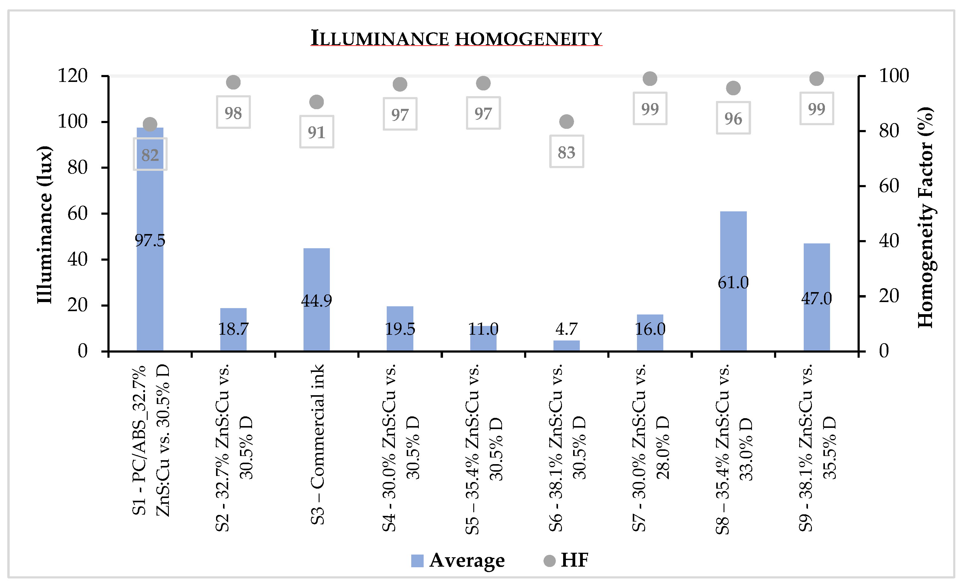
| 1 | S1 - 32.7% ZnS:Cu vs. 30.5% D | PC/ABS | 32.7 % | 30.5 % |
| 2 | S2 - 32.7% ZnS:Cu vs. 30.5% D | PES | 32.7 % | 30.5 % |
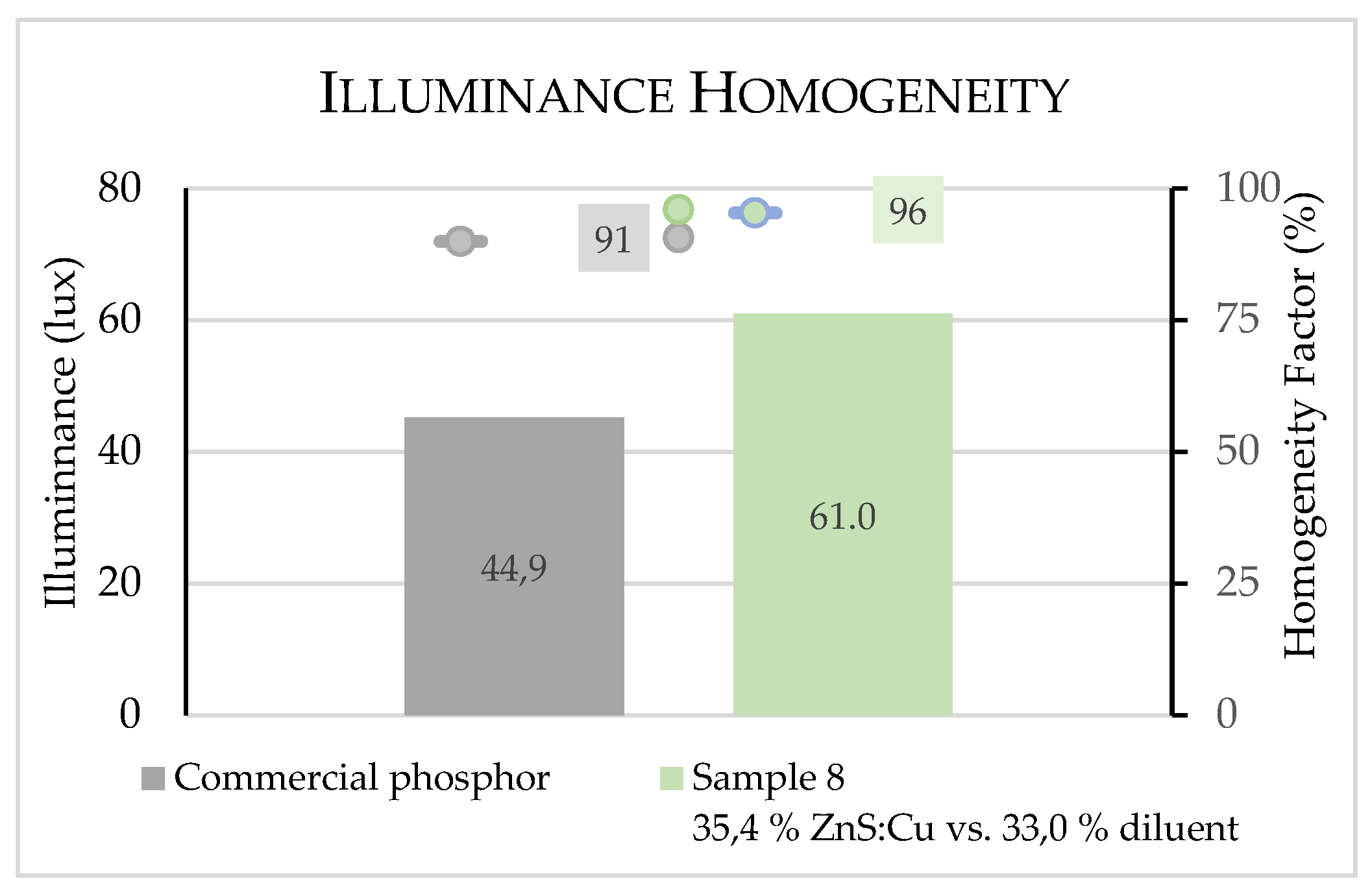
| 3 | S3 – Commercial ink | PES | LC-B311-GR-Lumigreen* | |
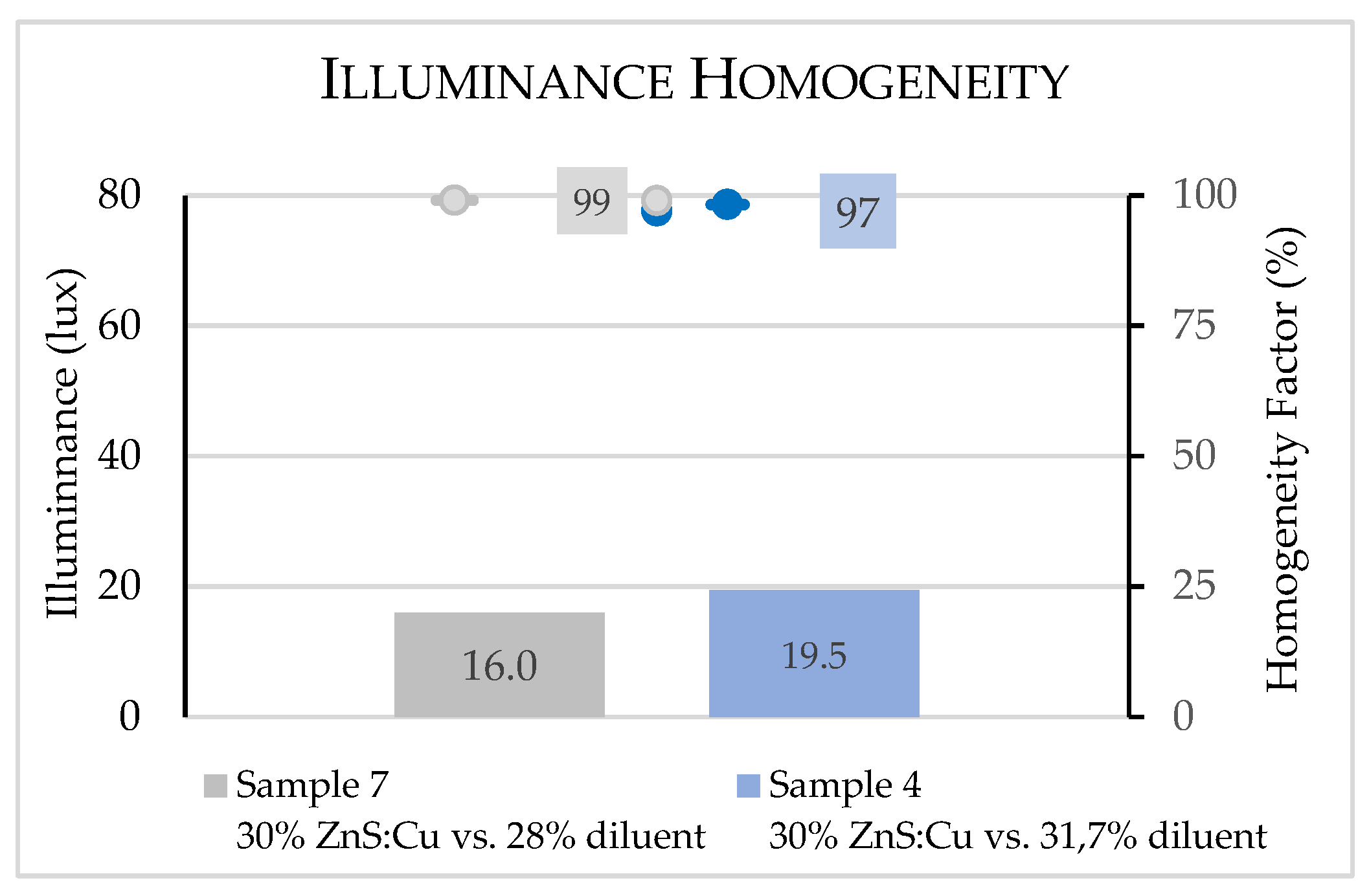
| 4 | S4 - 30.0% ZnS:Cu vs. 30.5% D | PES | 30.0 % | 30.5 % |
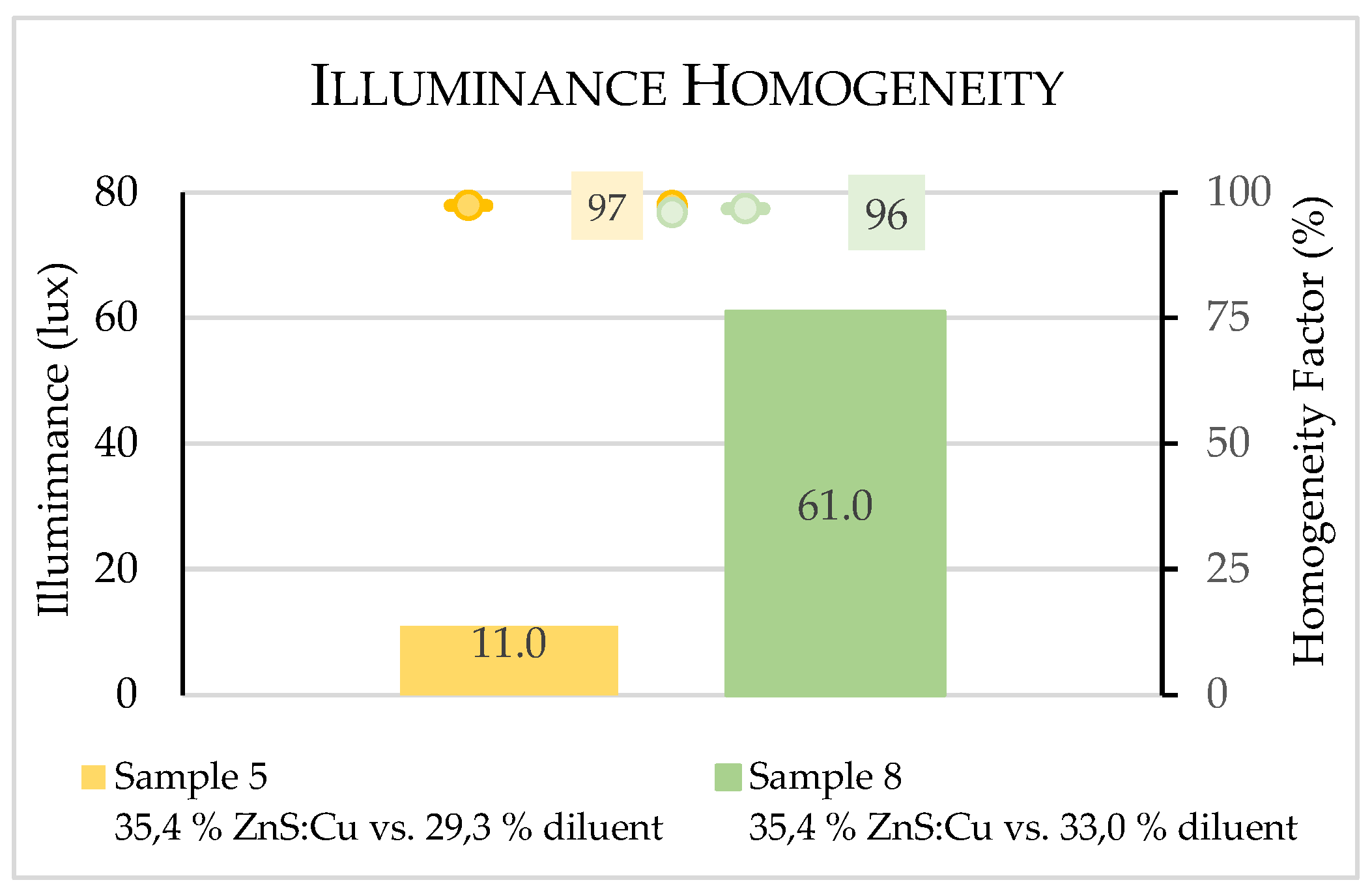
| 5 | S5 – 35.4% ZnS:Cu vs. 30.5% D | PES | 35.4 % | 30.5 % |
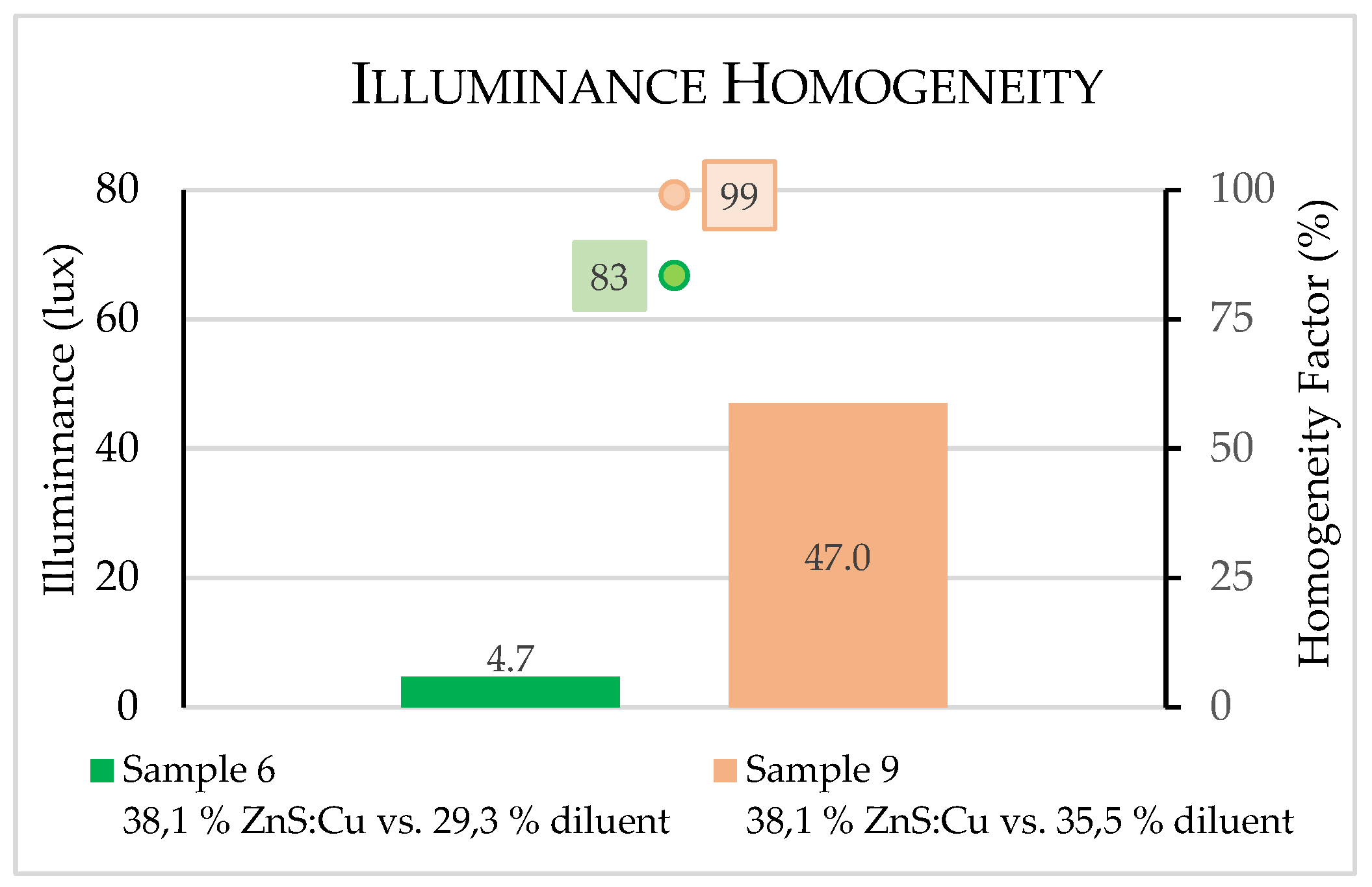
| 6 | S6 - 38.1% ZnS:Cu vs. 30.5% D | PES | 38.1 % | 30.5 % |
| 7 | S7 - 30.0% ZnS:Cu vs. 28.0% D | PES | 30.0 % | 28.0 % |
| 8 | S8 – 35.4% ZnS:Cu vs. 33.0% D | PES | 35.4 % | 33.0 % |
| 9 | S9 - 38.1% ZnS:Cu vs. 35.5% D | PES | 38.1 % | 35.5 % |
2.2. Methods
3. Results
3.1. Characterization by Scanning Electron Microscopy
3.2. Illuminance measurements
3.2.1. Performance evaluation of samples
3.2.2. Performance resume of all produced samples
| Element | Wt % |
| C | 53.05 |
| O | 4.77 |
| Al | 2.36 |
| S | 4.79 |
| Zn | 35.03 |
| Total | 100.00 |
3.3. Layer thickness analysis
4. Discussion
5. Conclusions
Author Contributions
Funding
Data Availability Statement
Acknowledgments
Conflicts of Interest
References
- Kathirgamanathan, P.; Bushby, L.M.; Kumaraverl, M.; Ravichandran, S.; Surendrakumar, S. Electroluminescent Organic and Quantum Dot LEDs: The State of the Art. J. Disp. Technol. 2015, 11, 480–493. [Google Scholar] [CrossRef]
- Fernández, M.R.; Casanova, E.Z.; Alonso, I.G. Review of Display Technologies Focusing on Power Consumption. Sustainability 2015, 7, 10854–10875. [Google Scholar] [CrossRef]
- Chansri, P.; Arunrungrusmi, S.; Yuji, T.; Mungkung, N. An Analysis of ZnS:Cu Phosphor Layer Thickness Influence on Electroluminescence Device Performances. Int. J. Photoenergy 2017, 2017, 1–4. [Google Scholar] [CrossRef]
- Kooroshnia, M.; Dumitrescu, D.; Lewis, E.; Walters, K. The colour, texture, and luminance: Textile design methods for printing with electroluminescent inks. Cultura e Scienza del Colore - Color Culture and Science 2023, 15, 27–34. [Google Scholar]
- Janczak, D.; Zych, M.; Raczyński, T.; Dybowska-Sarapuk, Ł.; Pepłowski, A.; Krzemiński, J.; Sosna-Głębska, A.; Znajdek, K.; Sibiński, M.; Jakubowska, M. Stretchable and Washable Electroluminescent Display Screen-Printed on Textile. Nanomaterials 2019, 9, 1276. [Google Scholar] [CrossRef] [PubMed]
- Graßmann, C.; Grethe, T.; van Langenhove, L.; Schwarz-Pfeiffer, A. Digital printing of electroluminescent devices on textile substrates. J. Eng. Fibers Fabr. 2019, 14. [Google Scholar] [CrossRef]
- Mi, H.; Zhong, L.; Tang, X.; Xu, P.; Liu, X.; Luo, T.; Jiang, X. Electroluminescent Fabric Woven by Ultrastretchable Fibers for Arbitrarily Controllable Pattern Display. ACS Appl. Mater. Interfaces 2021, 13, 11260–11267. [Google Scholar] [CrossRef] [PubMed]
- Verboven, I.; Deferme, W. Printing of flexible light emitting devices: A review on different technologies and devices, printing technologies and state-of-the-art applications and future prospects. Prog. Mater. Sci. 2020, 118, 100760. [Google Scholar] [CrossRef]
- Hu, B.; Li, D.; Ala, O. Prakash Manandhar. Qinguo Fan. Dayalan Kasilingam. Paul D. Calvert. Textile-Based Flexible Electroluminescent Devices. Advanced Functional Materials 2011, 21, 305–311. [Google Scholar] [CrossRef]
- Lumilor Basics and FAQ. Available online: https://support.lumilor.com/lumilor/lumilor-basics-and-faq#properties-of-lumilor-3 (accessed on 22th January 2023).
- Payne, S.A.; Moore, J.A. Preparation of Cross Sections of Difficult Materials for SEM Imaging. Microsc. Today 2018, 26, 40–45. [Google Scholar] [CrossRef]
- Policia, R.; Correia, D.M.; Perinka, N.; Tubio, C.R.; Lanceros-Mendez, S. Influence of polymer matrix on the luminescence of phosphor based printable electroluminescent materials and devices. Polymer 2023, 268. [Google Scholar] [CrossRef]
- Park, B.J.; Seo, H.S.; Ahn, J.T.; Song, J.H.; Chung, W.J.; Jeon, D.Y. An investigation on photoluminescence and AC powder electroluminescence of ZnS:Cu,Cl,Mn,Te phosphor. J. Mater. Res. 2011, 26, 2394–2399. [Google Scholar] [CrossRef]
- Fadavieslam, M.R. The effect of thickness of light emitting layer on physical properties of OLED devices. Optik 2019, 182, 452–457. [Google Scholar] [CrossRef]
- Mi, H.; Zhong, L.; Tang, X.; Xu, P.; Liu, X.; Luo, T.; Jiang, X. Electroluminescent Fabric Woven by Ultrastretchable Fibers for Arbitrarily Controllable Pattern Display. ACS Appl. Mater. Interfaces 2021, 13, 11260–11267. [Google Scholar] [CrossRef] [PubMed]
- Sloma, M.; Janczak, D.; Wroblewski, G.; Mlozniak, A.; Jakubowska, M. Electroluminescent structures printed on paper and textile elastic substrates. Circuit World 2014, 40, 13–16. [Google Scholar] [CrossRef]


Disclaimer/Publisher’s Note: The statements, opinions and data contained in all publications are solely those of the individual author(s) and contributor(s) and not of MDPI and/or the editor(s). MDPI and/or the editor(s) disclaim responsibility for any injury to people or property resulting from any ideas, methods, instructions or products referred to in the content. |
© 2023 by the authors. Licensee MDPI, Basel, Switzerland. This article is an open access article distributed under the terms and conditions of the Creative Commons Attribution (CC BY) license (http://creativecommons.org/licenses/by/4.0/).


