1. Introduction
Biosensors are analytical devices that integrate biological recognition elements with transducers to detect and quantify specific analytes in various sample matrices [
1,
2,
3]. These devices are widely used in a range of applications, including disease detection, medical diagnostics, drug selection, and environmental monitoring [
4,
5,
6,
7]. Recently, biosensors based on semiconductor materials is attracting more and more attention. This kind of biosensors offer numerous advantages over traditional analytical techniques, including high sensitivity, high specificity, and miniaturing capability [
8,
9].
Numerous two-dimensional (2D) semiconductor materials, such as nanowires, nanobelts, and nanotubes, find application in biosensing [
10,
11,
12,
13,
14]. The 2D materials are used in the devices serving as the transmission channel of carriers, and transducer devices employing these materials have demonstrated exceptional properties for detecting trace biomolecules, showcasing ultrahigh sensitivity. However, the critical challenge lies in addressing the stability and potential degradation induced by the solution when operating, given that these materials are exposed to ionic solutions [
15,
16]. Ensuring the accurate and reliable performance of biosensors over extended periods becomes imperative, despite their ultrahigh sensitivity. Solution-induced stability and degradation of biosensors made from 2D materials necessitate careful consideration, emphasizing the need to develop strategies that safeguard their performance in the presence of ionic solutions.
Biomedical sensors are designed to detect trace biomolecules within solutions, which can comprise various body fluids like blood, serum, urine, or buffered solutions [
17,
18]. These biosensors are subject to degradation over time due to various factors, including environmental conditions, surface chemistry, and biological interactions. Surface chemistry is one of the critical factors that can affect the stability of biosensors. The surface chemistry of the transducer material can significantly influence the interaction between the biological recognition element and the analyte [
19]. The adsorption of proteins, nucleic acids, and other biomolecules onto the transducer surface can interfere with the sensing mechanism and cause false reading results.
Stability issue stands as a pivotal concern when considering the performance of a transistor device. This concern becomes particularly pronounced when dealing with biosensor devices, as they are frequently employed in liquid environments. Unlike conventional transistor devices that typically operate in controlled environments safeguarded against moisture, light, and magnetic interference, biosensors must function within the context of trace biomolecule detection in solutions. These solutions often comprise various body fluids, such as blood, serum, urine, or buffer solutions. The extended immersion of biosensors in such solutions can accelerate the degradation of the transistor device itself, or even lead to the deterioration of its surface functionalization [
20,
21]. What further compounds the challenge is the high ion concentration present in these body fluids or buffer solutions. When a semiconductor biosensor device is immersed in such solutions, these ions can permeate the device, raising concerns related to the device's reliability [
22,
23].
In light of these considerations, it becomes imperative to conduct a time-dependent stability assessment of the 2D materials based biosensors when immersed in a buffer solution. Such an evaluation is vital to ascertain the device's ability to maintain consistent and reliable performance over time. Literature concerning about the solution induced stability is, however, little reported. Therefore, this study aims to uncover the longevity and resilience of the biosensor device when subjected to the complex and dynamic conditions of a liquid environment.
This paper details the fabrication of a silicon nanobelt field effect transistor (NBFET) device using a commercially available CMOS-compatible manufacturing technique. Diverging from traditional Planar FET devices, the NBFET employs a narrow and thin nanobelt as a channel to establish the connection between the source and drain. This unique design imparts ultrahigh sensitivity to the NBFET biosensor, particularly in the detection of biomolecules. The fabricated NBFET device was specifically employed for the detection of DNA strands. Subsequently, this NBFET biosensor underwent immersion in a buffer solution, and its electrical properties were systematically monitored to assess the solution-induced stability of the device. The investigation into the device's performance over prolonged periods in challenging environments provides valuable insights into its durability and efficacy as a stable and robust sensing tool. The outcomes of this study not only contribute to the broader field of biosensors but also establish a foundational reference for future advancements in biomedical devices. By elucidating the solution-induced stability of the NBFET biosensor, this research paves the way for improved understanding and innovation in the development of reliable and enduring sensing technologies for various biomedical applications.
3. Results and Discussions
We used a TEM (JEM-2010F, JOEL Ltd., Tokyo, Japan) to observe the structure of the nanobelt.
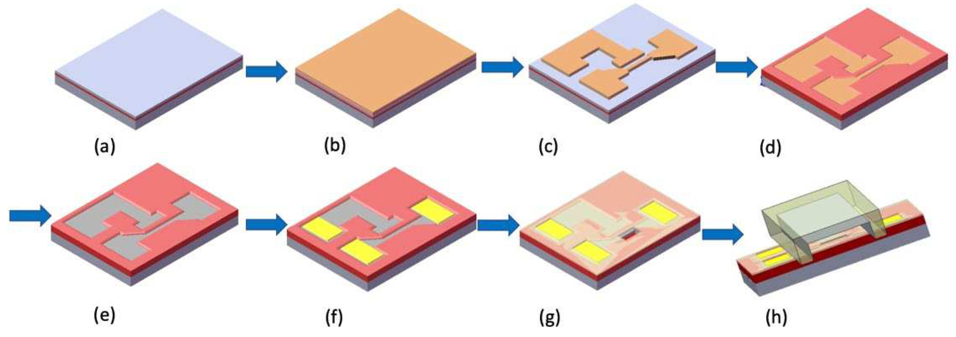
Figure 3(a) presents a cross-sectional image of the silicon nanobelt, revealing key structural details. Notably, the width of the nanobelt underwent a significant reduction, diminishing from its original dimensions of 350 nm to a slender 150 nm. Moreover, the initial thickness of 50 nm experienced a substantial decrease to approximately 5 nm following the LOCOS processing, as visually demonstrated in the figure. It's imperative to underscore that the local-oxidation of silicon process, as shown in
Figure 1(d), is of critical importance to the formation of the nanobelt. This transformation in the nanobelt's dimensions is intricately linked to the oxide thickness in the local-oxidation process. Not only does the oxidation process validate the complete oxidation of the underlying silicon, but also ensures the preservation of the nanobelt's original thickness. This meticulous control over the structural changes in the nanobelt plays a pivotal role in enhancing the sensitivity of the NBFET biosensor. The improved sensitivity of the NBFET sensor is attributed to the substantial reduction in dimensions while retaining a substantial detection region on the surface. This combination of factors contributes to the sensor's heightened capability to detect and respond to subtle changes in its surroundings.
The morphology of the NBFET device was demonstrated through FESEM (JSM-6700F, JOEL Ltd., Tokyo, Japan).
Figure 3(b) presents top-view image of the NBFET device, including source, drain, side-gate, and nanobelt. The length of the nanobelt in our design was 30 μm-long. The side-gate was designed in the NBFET biosensor to provide an in- dividual gate voltage for each device, and hence ensure its controllable and stable properties.
Figure 3.
(a) Cross-sectional TEM images of the formed silicon nanobelt. (b) Top-view FESEM image of the NBFET structure.
Figure 3.
(a) Cross-sectional TEM images of the formed silicon nanobelt. (b) Top-view FESEM image of the NBFET structure.
To exam the electrical characteristics of the side-gates NBFET devices, the drain current versus gate voltage (
ID–
VG), as well as drain current versus drain voltage (
ID–
VD), were measured before biosensing applications. The
ID–
VG and
ID–
VD curves serve as crucial indices for assessing the characteristics of a transistor device. Prior to electrical measurements, PBS was introduced through the microfluidic channel and subsequently remained on the nanobelt surface. It is noteworthy that the detection area was selectively opened on a segment of the nanobelt, as depicted in
Figure 1(g). The remaining portion of the entire device was shielded by a Si
3N
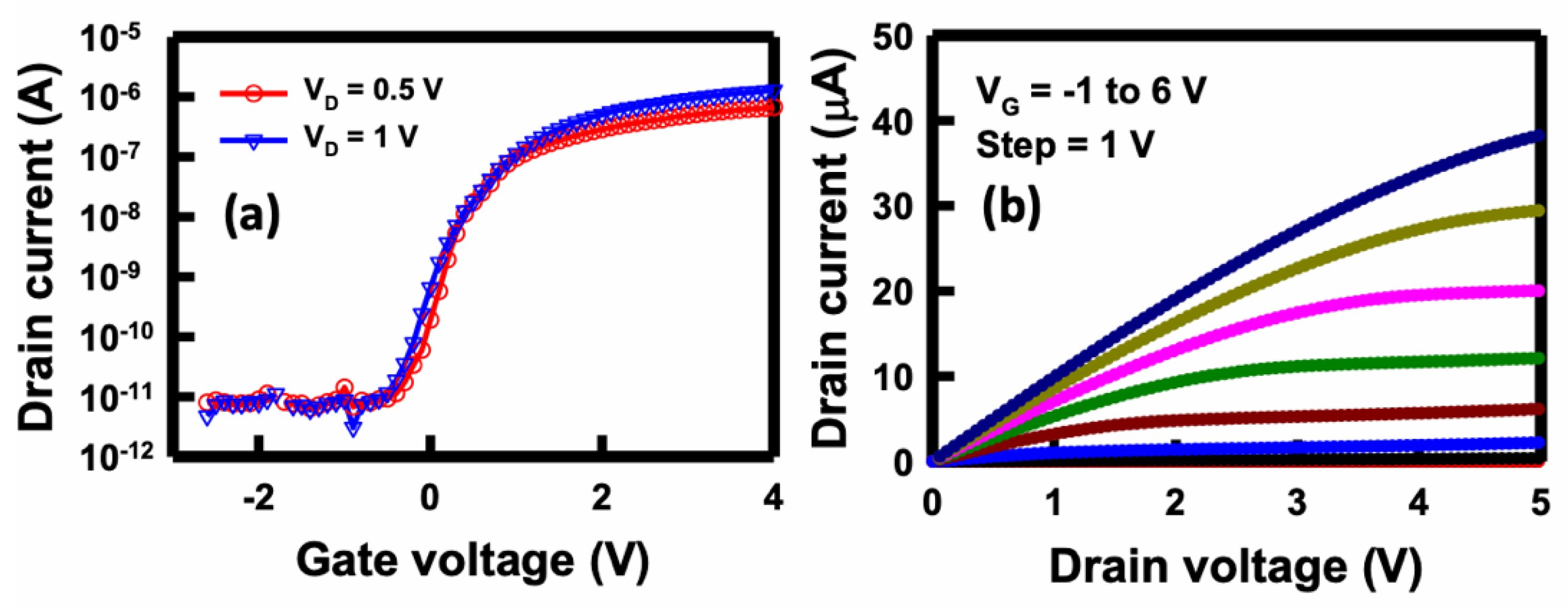
4/oxide film. In this configuration, only the nanobelt came into contact with PBS, ensuring that the gate, drain, and source electrodes remained unaffected by the solution. The fundamental electrical performance of the transistor device is of paramount importance, as it directly impacts the biosensor's sensitivity, limit of detection (LOD), as well as its stability and reliability when employed as a biosensor. In
Figure 4(a), we present the
ID–
VG plot at
VD of 0.5 and 1 V, respectively. This plot illustrates the ability to switch the current I
D flowing through the nanobelt, from 10
-11 to 10
-6 A, at various side gate potentials. Under a substantial negative gate voltage, such as –2 V, the channel conduction is notably low. When applying a positive voltage to the gate, such as 2 V, it creates an electron channel, rendering the transistor a normally-on, and thus the current increases. In practice, the side gate can apply an electric field to the nanobelt, thus influencing the energy band for the charge carriers. The sensor's practicality is further highlighted by the on/off current ratio, which approaches five orders of magnitude when V
D is applied on 1 V. The determined threshold voltage (
Vt) can be extracted to approximately 0.5 V, and the subthreshold swing (SS) is calculated to be 150 mV/decade. This substantial ratio suggests the enhanced utility of the fabricated NBFET biosensors, which can be attributed to the heightened sensitivity.
Figure 4(b) depicts the
ID–
VD curves of the NBFET device across a range of applied V
G values, spanning from -1 to 6 V. It is observed that the
ID increases obviously when
VG is increasing, whereas only a modest increase with increasing
VD. The result of this figure highlights the distinctive behavior of
ID concerning
VD and
VG for the NBFET device, which indicates the primary factor influencing the current is the variation in
VG. Therefore, the judicious selection of an appropriate gate voltage becomes imperative to operate the device under the most favorable conditions for subsequent biosensing applications. Understanding the interplay between
VG,
VD, and
ID in this NBFET device is pivotal for optimizing its performance as a biosensor. By strategically adjusting the gate voltage, it becomes feasible to precisely modulate the device's current response, enhancing its sensitivity and reliability in biosensing applications.
Figure 4.
Fundamental electrical characteristics of the NBFET device. (a) ID–VG curves at VD= 0.5 and 1 V, and (b) ID–VD curves at VG from -1 to 6 V.
Figure 4.
Fundamental electrical characteristics of the NBFET device. (a) ID–VG curves at VD= 0.5 and 1 V, and (b) ID–VD curves at VG from -1 to 6 V.
The stability of the NBFET device, especially when utilized as a biosensor in complex liquid environments, is a critical consideration. The challenges posed by extended exposure to buffer solutions, along with the presence of ions, necessitate a thorough investigation into the stability of the biosensor device. This endeavor is fundamental to ensuring the device's reliability and effectiveness in real-world biomedical applications, where precise and consistent results are of utmost importance.
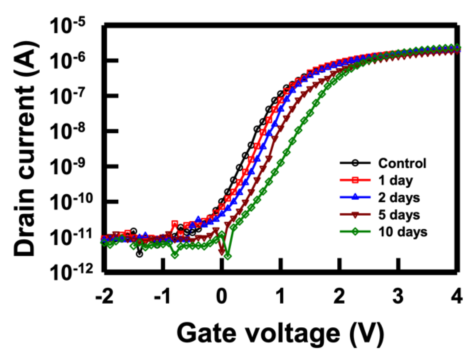
Given these intricate challenges, it is imperative to conduct a time-dependent stability assessment of the NBFET device when immersed in a buffer solution. This evaluation allows us to gain insights into how the device's performance evolves over time in real conditions. Illustrated in
Figure 5 are the
ID–
VD curves of the NBFET biosensor immersed in PBS over varying durations. Evidently, the curves gradually shift right with increasing immersion days. Notably, the SS experiences a slight change after 5 days, becoming significantly smaller after 10 days of immersion. This observation underscores the impact of the buffer solution on the electrical characteristics of the NBFET device, revealing a heightened degradation as the immersion duration extends. These findings emphasize the necessity of understanding and addressing the time-dependent stability challenges in biosensor applications.
Figure 5.
ID–VD curves of the NBFET biosensor immersed in PBS over varying durations.
Figure 5.
ID–VD curves of the NBFET biosensor immersed in PBS over varying durations.
To comprehend the underlying mechanism behind the degradation induced by the buffer solution, we conducted a thorough analysis of the electrical characteristics of NBFET biosensors immersed in PBS solutions with varying concentrations.
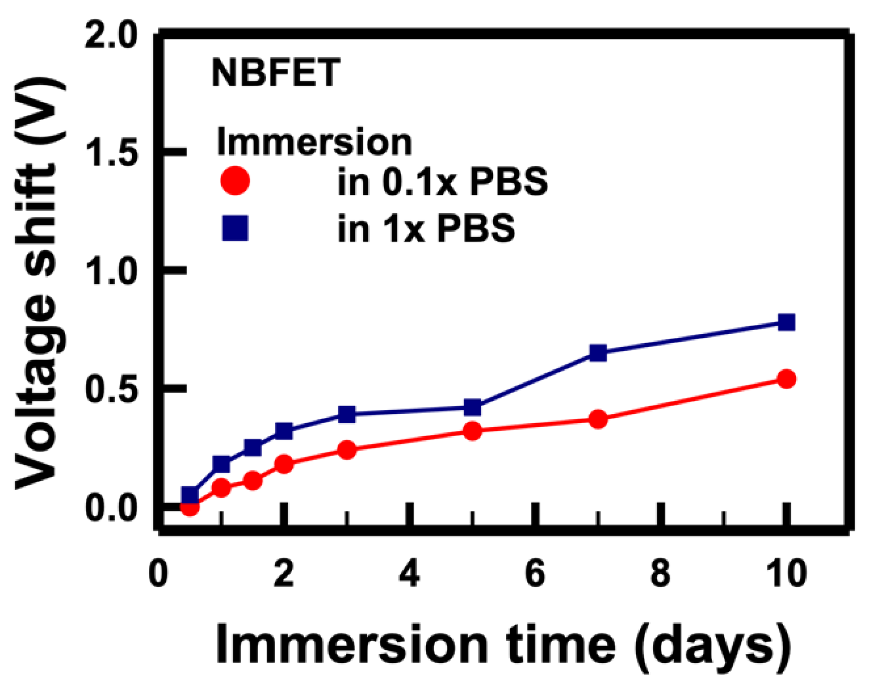
Figure 6 illustrates the voltage shifts of NBFET devices immersed in original 10 mM (denoted as 1×) and diluted 1 mM (denoted as 0.1×) concentrations, respectively. The calculation of voltage shift involved utilizing the drain current associated with the control
Vt value (
Vt, Control) of the NBFET biosensor device as the baseline current. This reference current was then incorporated into the curves for different immersion durations to derive the immersed
Vt value (
Vt, Immerse). The formula for this calculation is as follows:
The results show that, regardless of whether the devices were immersed in 1× or 0.1× solutions, the voltage shifts increased with prolonged immersion days, aligning with the trends observed in
Figure 5. Remarkably, a higher magnitude of voltage shifts was observed in the 1× PBS sample compared to the 0.1×. This discrepancy can be attributed to the tenfold higher ion concentration in the 1× PBS compared to the 0.1×. From this, we infer that the primary cause of NBFET degradation is the penetration of ions into the nanobelt structure. This understanding sheds light on the critical role of ion penetration in the observed degradation of NBFET devices immersed in buffer solutions, further emphasizing the importance of addressing this challenge for enhanced device reliability and longevity.
Figure 6.
Voltage shifts of the NBFET biosensors immersed in PBS solutions with different concentrations over varying durations.
Figure 6.
Voltage shifts of the NBFET biosensors immersed in PBS solutions with different concentrations over varying durations.
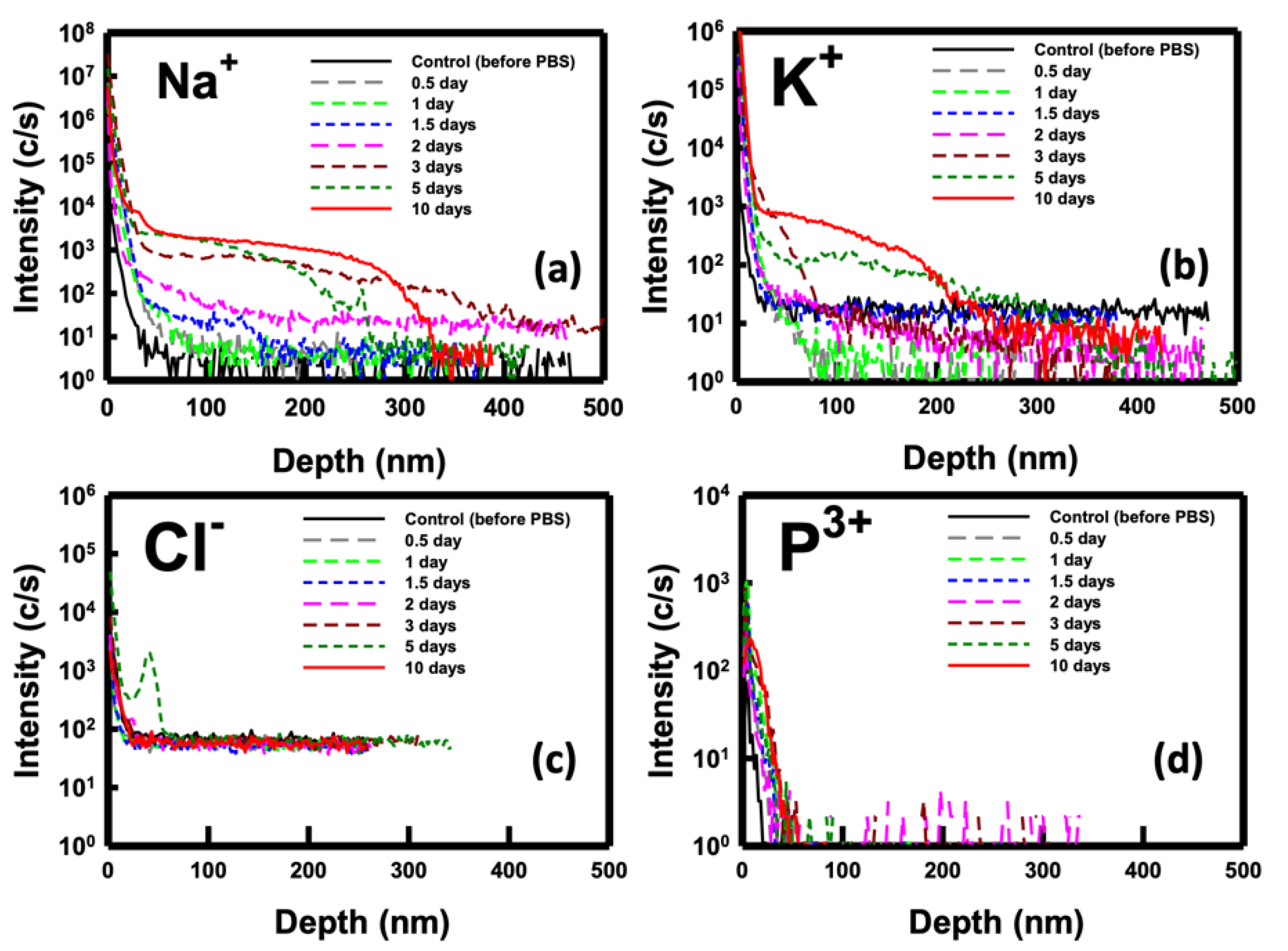
To elucidate the phenomenon of ion penetration during the immersion period, we employed SIMS (CAMECA IMS 7F, AMETEK, Inc., Gennevilliers, France) analysis for monitoring purposes. Analyzing the key ions present in the PBS buffer solution, namely sodium (Na
+), potassium (K
+), chlorine (Cl
–), and phosphorous (P
3+), we conducted a thorough investigation.
Figure 7 depicts the SIMS depth profiles of these ions for samples immersed in PBS for durations ranging from 0.5 to 10 days. The results obtained highlight the penetration of Na
+ and K
+ ions into the substrate post-immersion, with no observable penetration for Cl
– and P
3+ ions. Specifically, Na
+ ions exhibited slight penetration into the substrate after 2 days, intensifying from days 3 to 10. In contrast, noticeable penetration of K
+ ions was observed after 5 days of immersion. These findings from the SIMS analysis align with the previously discussed electrical properties of the NBFET devices.
Figure 7.
SIMS depth profile of the ions for the sample immersed in the PBS solution over various durations. (a) Sodium ions, (b) potassium ions. (a) chlorine ions, and (a) phosphorus ions.
Figure 7.
SIMS depth profile of the ions for the sample immersed in the PBS solution over various durations. (a) Sodium ions, (b) potassium ions. (a) chlorine ions, and (a) phosphorus ions.
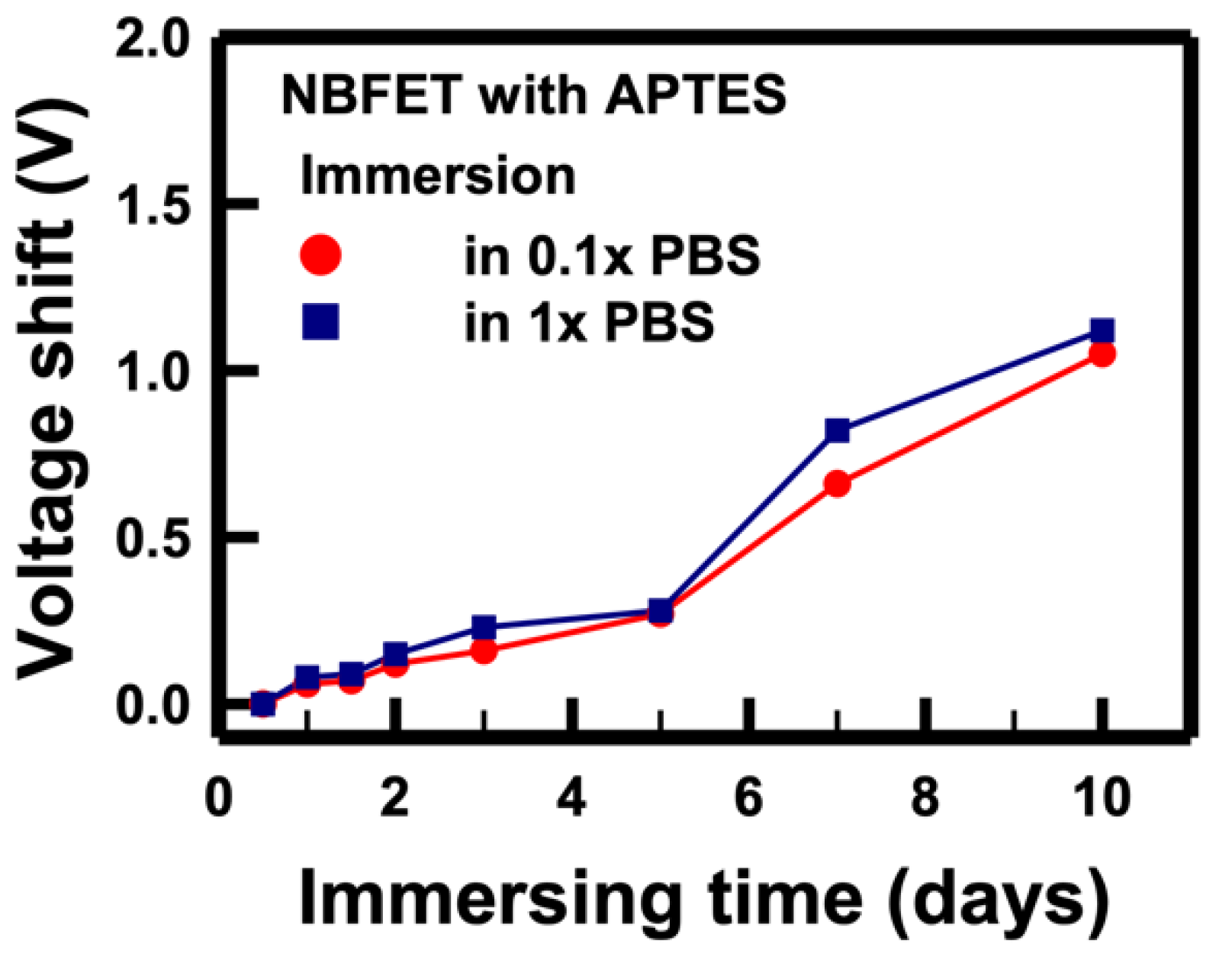
The electrical performance of NBFET biosensors featuring APTES coating on the nanobelt surface was also assessed to evaluate their effectiveness following PBS immersion. In
Figure 8, the voltage shifts of APTES-functionalized NBFET biosensors immersed in 1× and 0.1× PBS buffers are illustrated. Notably, for samples subjected to less than 5 days of immersion, APTES-functionalized NBFET devices exhibited smaller voltage shifts compared to their uncoated counterparts. However, the voltage shifts of APTES-functionalized NBFET devices showed a significant increase during immersion from 7 to 10 days. Furthermore, the discrepancy in voltage shifts between 1× and 0.1× PBS conditions was found to be smaller for the APTES-functionalized samples compared to the uncoated ones. This observation leads us to conclude that, within the initial 5 days of immersion, ions' penetration may influence the performance of NBFET devices. Beyond this period, however, ions' penetration is not the predominant mechanism causing voltage shifts in the APTES-coated samples. These findings underscore the temporal dynamics of APTES coating effectiveness in mitigating ion-induced effects on NBFET device performance.
Figure 8.
Voltage shifts of the APTES-functionalized NBFET biosensors immersed in PBS solutions with different concentrations over varying durations.
Figure 8.
Voltage shifts of the APTES-functionalized NBFET biosensors immersed in PBS solutions with different concentrations over varying durations.
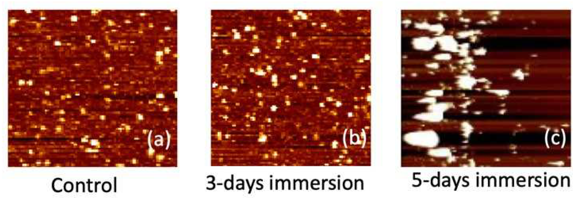
In
Figure 9, AFM images depicting the APTES-coated samples are presented for intervals of 0, 3 days, and 5 days of PBS immersion. The presence of white spots in the images signifies chemical molecules binding to the surface. Following a 3-day immersion, the number of white spots noticeably increases. Notably, after 5 days of immersion, the size of these white spots undergoes a substantial increase, forming clusters on the sample surface. We hypothesize that these white clusters result from APTES peeling off after prolonged immersion in the PBS solution. This supposition aligns with the electrical measurement results showcased in
Figure 8. Given the positively charged nature of the APTES film, the peeling off of the film induces a rightward shift in the
ID–
VG curve of the NBFET device, leading to an increase in
Vt. This correlation between AFM observations and electrical measurements provides valuable insights into the impact of prolonged PBS immersion on the APTES-coated samples, further underlining the intricate dynamics between surface modifications and device performance.
Figure 9.
Surface AFM images of the APTES-coated samples for (a) control (0 day), (b) 3 days, and (c) 5 days of PBS immersion.
Figure 9.
Surface AFM images of the APTES-coated samples for (a) control (0 day), (b) 3 days, and (c) 5 days of PBS immersion.
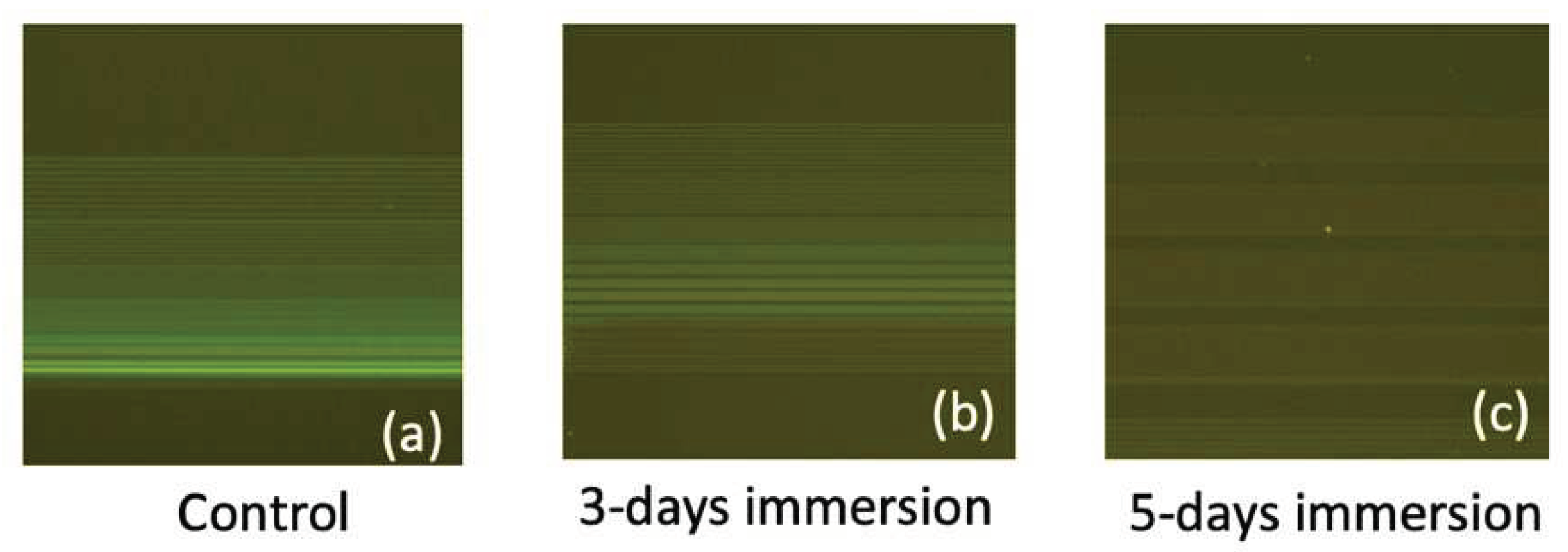
In
Figure 10, fluorescence images depicting FITC-labeled DNA strands bonded to the SiO
2 line patterns are presented for immersion durations of 0, 3 days, and 5 days in PBS. The attachment of DNA strands to the SiO
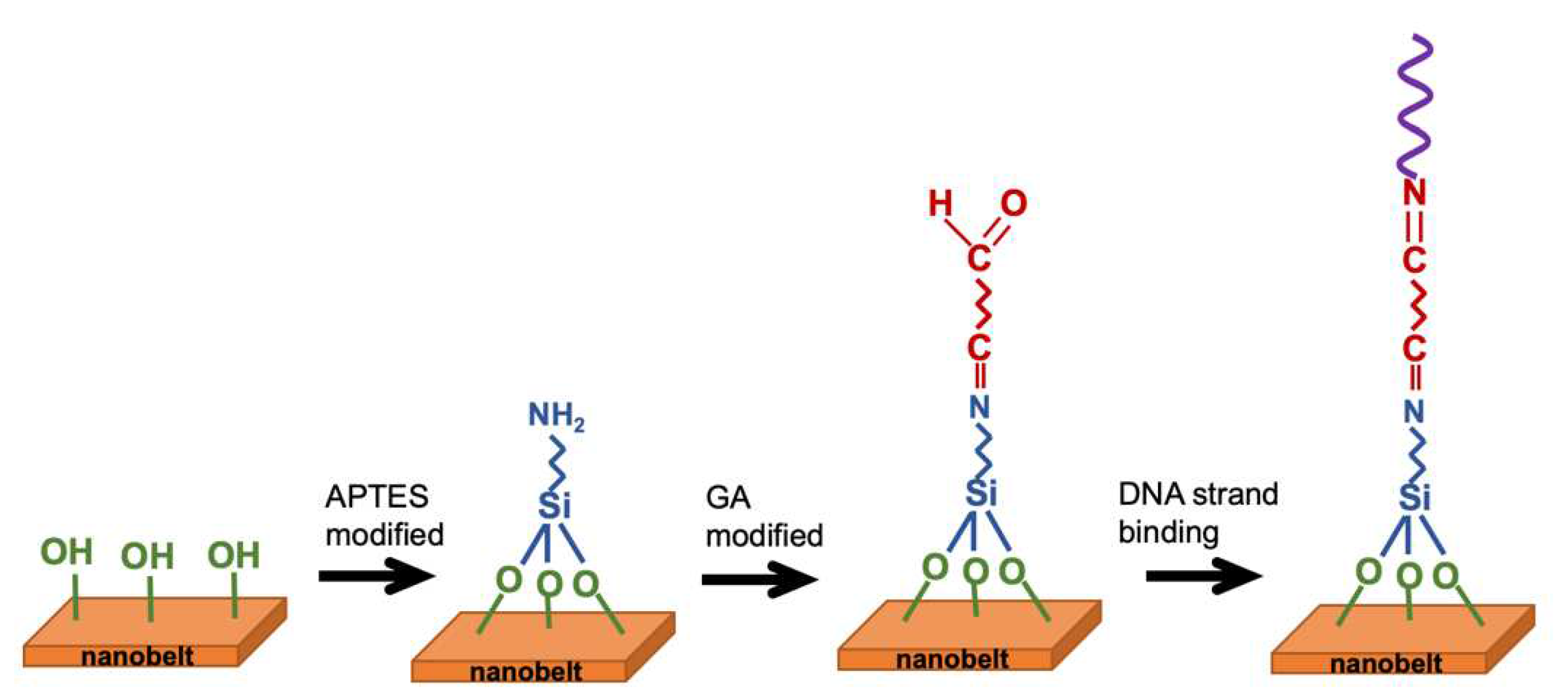
2 line patterns was facilitated through amine and carboxyl interactions, achieved via the APTES and GA functionalization process. Notably, the control sample exhibits the highest and most distinct fluorescence intensity, indicating a high binding efficiency of DNA strands to the SiO
2 substrate. However, the fluorescence intensity decreases as the immersion duration increases. By integrating the results from AFM and fluorescence images, we can deduce that prolonged PBS immersion induces the peeling off of the APTES film, consequently degrading the binding efficiency of biomolecules. This comprehensive analysis underscores the intricate interplay between surface modifications, biomolecule binding, and the environmental factors affecting biosensor performance over time.
Figure 10.
Fluorescence images of the FITC-labeled DNA strands bonded to the SiO2 line patterns for PBS immersion durations of (a) control (0 day), (b) 3 days, and (c) 5 days.
Figure 10.
Fluorescence images of the FITC-labeled DNA strands bonded to the SiO2 line patterns for PBS immersion durations of (a) control (0 day), (b) 3 days, and (c) 5 days.
