I NTRODUCTION
HE increasing demand for high-speed communication has urged researchers to develop new communication systems. Currently, wireless data transmission higher than one gigabits-per-second (Gbps) data rate is essential due to internet-enabled devices’ proliferation. The spectrum at 60GHz range, reserved internationally for industrial, scientific, and medical (ISM) band with an available 9GHz unlicensed bandwidth, draws much attention. There have been significant research efforts towards the 60GHz applications related to high data-rate wireless communications.
The high-performance, high-data-rate 60GHz transceivers are reported in [
1,
2,
3,
4]. The designs [
1,
2] target the next- generation WiFi standard 802.11ay with wider bandwidth and higher-order modulation. The work in [
1] presents an area-efficient bidirectional transceiver that utilizes a bi-directional amplifier to entirely share the mixer and LO between transmitter and receiver modes. The measured link error vector magnitude (EVM) for a single channel is -24.3dB for 16-QAM at 0.12m. In [
2], a single transceiver with 50.1Gbps with 8.35GSym/s in 64-QAM and 3.52GSym/s with 128-QAM modulation is reported. The reported single-channel communication with 64-QAM in 0.15m achieves EVM of -28.2dB. In [
3], a low power, small size on-off keying (OOK) transceiver is reported with 12.5Gbps with energy efficiency at 2.65pJ/bit. All the reported works in [
1,
2,
3] suffer from shorter communication distances limited by the noise floor bandwidth, and they all rely on half-duplex (HD) operation only. The work in [
4] presents 2×64 and 2×256 elements dual polarization transceiver arrays with a maximum equivalent isotropic radiated/ power (EIRP) of 38dBm and 44dBm, respectively. It gives good signal coverage but consumes large chip area and power consumption.
The FD operation is another way to deliver high data rate by doubling the system’s achievable spectrum efficiency [
5,
6]. Moreover, the ultra-low latency demand for the upcoming wireless communication system [
7] is another benefit for the FD system. With optical communication like propagation characteristics and narrow beam width makes it a good candidate for a 60GHz transceiver to work in FD mode. However, the FD system suffers from an enormous RF signal power difference between the power imposed by its transmission and that received from the remote transmitter.
Self-interference (SI) suppression or cancellation is critical for an FD system. The work in [
8] presents a 60GHz transceiver with a polarization-based antenna with RF cancellation. It achieves SI suppression of 70dB from the transmitter to its receiver. The work in [
9] involves SI cancellation for FD transceiver in a single antenna system. It achieves 40dB SI cancellation by using an RF circulator to separate transmitter and receiver and a reconfigurable impedance mismatched circuit to modify the frequency response of the SI channel. The work in [
10] demonstrates an E-band backhaul solution achieving 8Gbps under the frequency division duplex (FDD) mode. The isolation between transmitter and receiver is greater than 50dB. However, those active RF frontend cancellation-based FD systems involve complex circuit design and work for specified bandwidth only.
This paper proposes a low power 60GHz transceiver prototype that is fully compatible with IEEE 802.11ad wireless standard. Other than the traditional IEEE 802.11 WiFi standards, which works in HD mode, the work supports both FDD and FD operations. Additionally, the system supports hybrid schemes with reconfigurable switching between HD, FDD and FD operation mode. The proposed system’s SI requirements are relaxed compared to the works in [
8,
11] due to low transmission power for a comparable communication distance.
The organization of this paper is as follows: Section II describes the design challenges of the proposed transceiver through the link budget estimation. Section III introduces the design and implementation of some critical components in the prototype system. In Section IV, the integrated transceiver measurement is shown. Finally, in Section V, conclusion is presented.
II SYSTEM REQUIREMENT
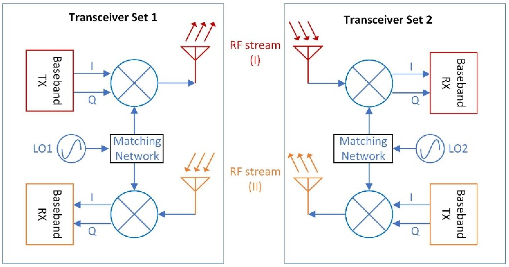
Figure 1 shows the simplified diagram of the proposed system with two transceiver sets. In HD mode, one transceiver is configured as transmitter and the other as receiver. Since they are always working in opposite mode, and there is only one RF stream available all the time, it is also named as time division duplexing (TDD). While in frequency division duplex (FDD) or in-band full-duplex (FD) mode, both transceiver sets act as transmitter and receiver simultaneously. Two RF streams are available in the opposite direction, and they can be configured with either the same or different carrier frequencies. In FDD, different carrier frequencies are used while in FD, the same carrier frequency is used.
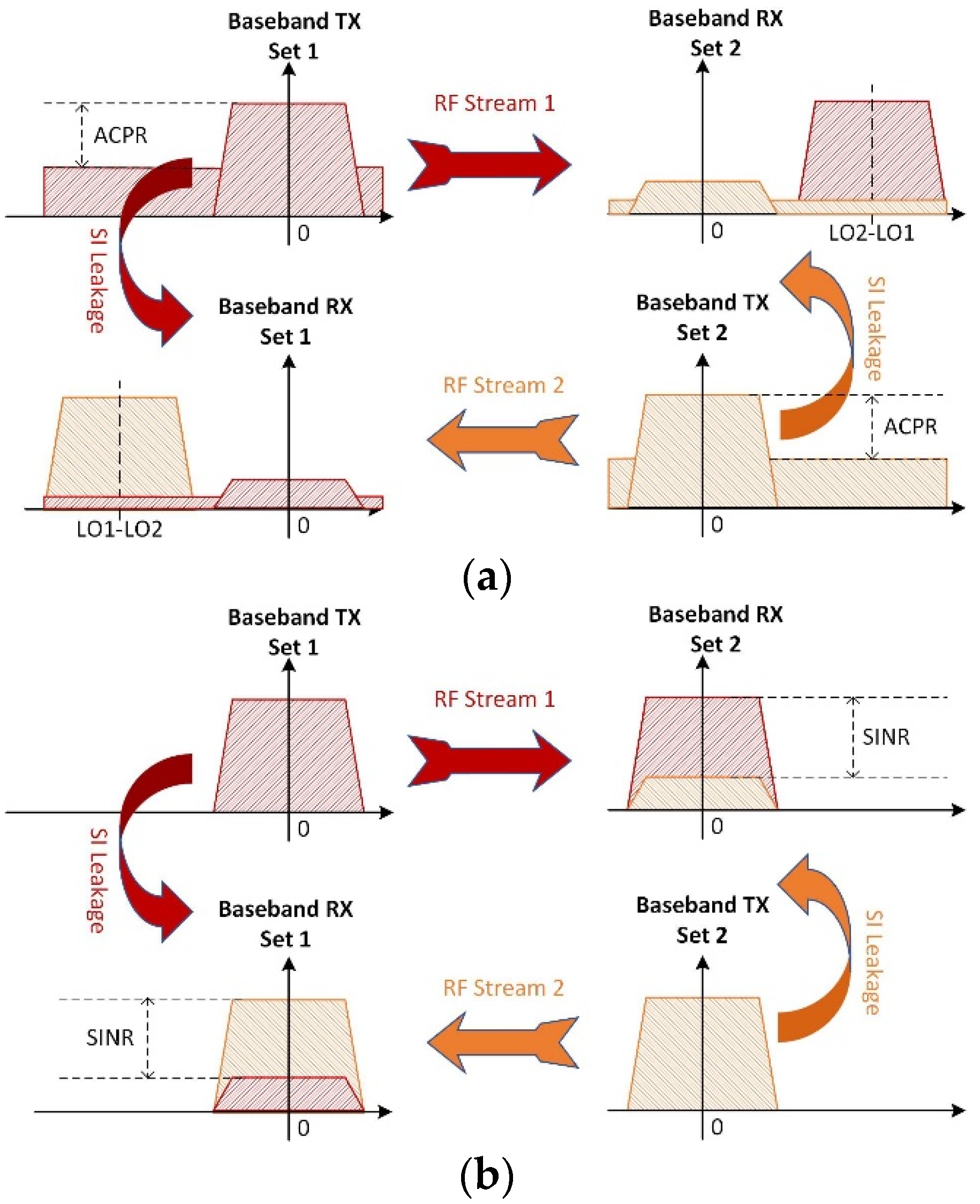
Figure 2(a) and
Figure 2(b) show the spectrum conversion for both FDD and FD modes.
In the FDD operation shown in
Figure 2(a), LO frequencies are set at LO1 and LO2 so that the transmitter and receiver are separated in the frequency domain. It is achieved by adopting wide bandwidth amplifiers in the receiver chain to cover its adjacent band. The wanted signals are separated from the SI signal in the frequency domain, and it can be recovered using a high-pass filter. The adjacent channel power ratio (ACPR) and SI isolation are the dominant considerations for FDD operation. However, the channel utilization is low as both transceivers occupy a separate physical channel. The digital baseband processor needs to handle the signal with IF carrier, which will increase the complexity of the data processing units. In the FD mode, as shown in
Figure 2(b), both transceivers work simultaneously at the same channel such that, two RF streams share the physical channel but are in opposite directions. In this mode, frequency reuse strategy can theoretically double the spectral efficiency. The technical difficulties for such an approach are the requirement for SI suppression or cancellation, as SI and the wanted signal overlapped at baseband. An excessive SI may even result in a reduced capacity for the FD system that falls below the HD systems. As shown in
Figure 2(b), the signal-to-interference and noise ratio (SINR) is the key parameter to estimate the capability of FD system. In principle, SI can be perfectly regenerated and compensated since the transmitted data is known inside the transceiver. However, realistic SI is also affected by non-linear effects of the transmitter and receiver chain, and unpredictable LO phase noise that makes it far from the estimation.
A. Link Budget Model
The proposed transceiver is targeted for the IEEE 802.11ad wireless standard up to a communication distance of 3m. It can support MCS12 scheme under traditional WiFi operation. The highest raw data rate is 7.04Gbps under 1.76GSym/s of 16-QAM with EVM at -21dB. A wideband signal results in an increased in-band noise floor and reduces the SNR. The noise floor can be estimated by using the thermal noise for the given channel bandwidth together with the additional receiver noise figure and some implementation losses. Considering a 2.16GHz channel bandwidth, an additional 5dB budget for the receiver chain’s noise figure and 5dB implementation losses, the noise floor of the receiver system will be -70.6dBm theoretically.
Table 1 lists the EVM requirement for some of the key modulation schemes defined in WiFi standard [
12], with the receiver sensitivity level for the system based on the estimated noise floor. As listed in the table, the received signal power at the LNA input must be higher than -49.6dBm because of the 21dB minimal EVM requirement for the targeted modulation scheme at MCS12. To further increase the systems’ data rate, either a higher-order modulation scheme or a lower error code rate is required, as can be seen for MCS12.1 to MCS12.6, but with an increased SNR requirement.
The reference-free space loss for the 60GHz signal is around 68dB at 1m distance [
13,
14]. In this estimation, the additional attenuation items can be ignored because multipath fading effect is insignificant due to short communication distance, narrow beamwidth, and good alignment of antennas. A pair of narrow beam directional antennas are designed and integrated on the RF printed circuit board (PCB) to simplify the system integration and reduce the prototype cost. The integrated antenna provides 12dBi antenna gain for both transmitter and receiver with 17
◦half-power beam coverages. The propagation loss for the system reduces to 53.6dB with the help of such directional antennas. As mentioned in
Table 1, the EVM requirement for MCS-12 is -21dB and the received power must be larger than -49.6dBm. With a 53.6dB propagation loss, the transmitter’s output power should be larger than +4dBm to satisfy the minimum received power requirements.
To support a higher modulation scheme with variable amplitude, such as 16-QAM and 64-QAM, a peak-to-average power ratio (PAPR) budget is needed to ensure the linearity of the modulated signal. This can be realized by either increasing the output power of the transmitter or reducing the communication distance to support those high order modulation schemes.
B. System Architecture
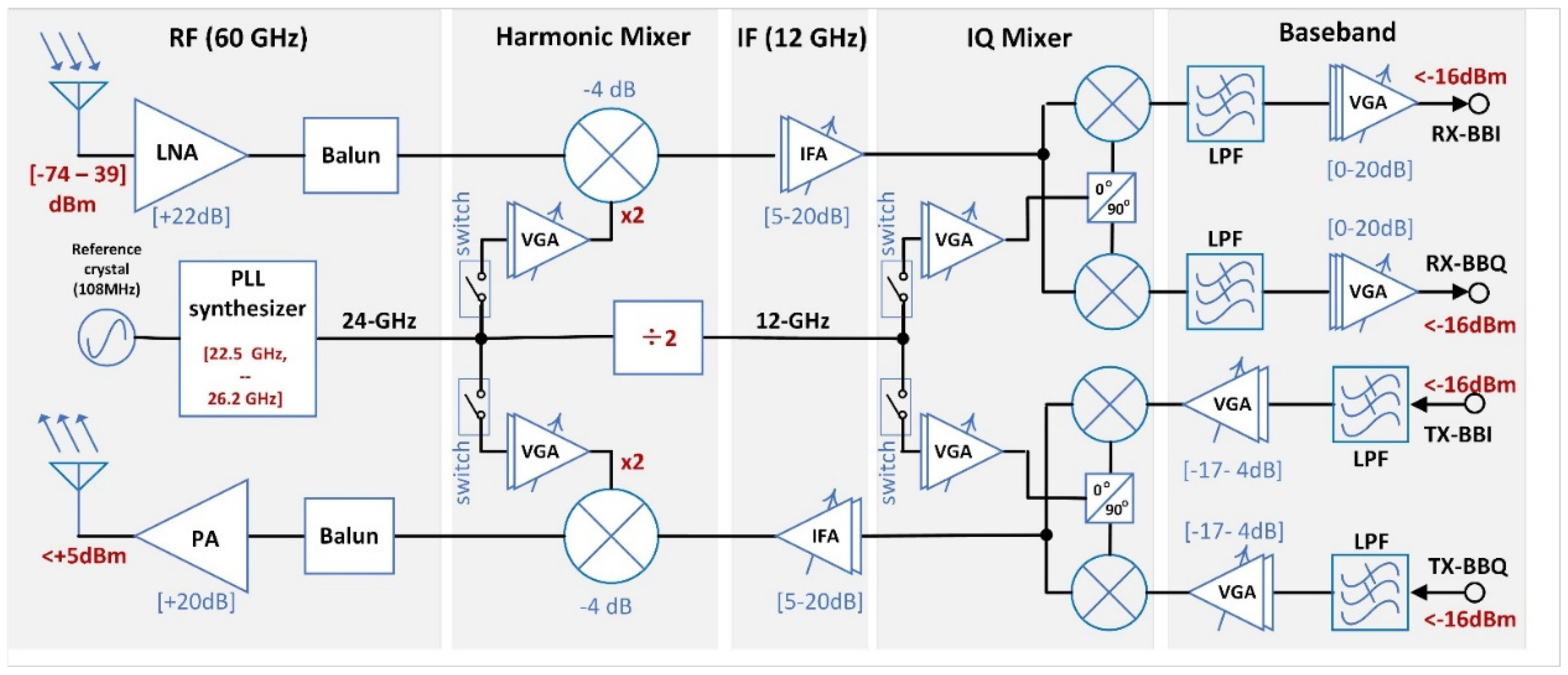
The transceiver architecture of the proposed system is shown in
Figure 3 [
15,
16]. It is a super-heterodyne transceiver with two stages of frequency conversion. The sufficiently high intermediate frequency (IF) helps the low noise amplifier (LNA) and power amplifier (PA) to suppress the image components by their bandwidth characteristics. This architecture also re-quires only one phase locked loop (PLL) synthesizer to complete all frequency conversion and achieve a low power con-sumption.
In the receiver chain, a sub-harmonic mixer is used as the first stage down-conversion mixer. The input signal is mixed with a local oscillator at 4/5 of RF frequency to generate the down converted IF signal to 1/5 of the RF frequency. The sec-ond stage is a quadrature I/Q mixer to further down-convert the IF signal to the quadrature baseband. A 90◦ hybrid is uti-lized to generate the orthogonal LO signal. Finally, the I/Q mixer’s output passes through a low-pass filter and a dB-linear digital variable gain amplifier (DVGA) before the digital baseband for further processing. The amplitude imbalance can be compensated by fine-tuning the gain of baseband DVGA and the matched hybrid minimizes the phase imbalance across the frequency bands of interest. The overall variable gain in the receiver chain is from 23dB to 58dB. The saturation output power of the baseband DVGA in the receiver chain is -16dBm for both the I and Q path. The input power range for the re-ceiver should be chosen between -74dBm and -39dBm.
The transmitter chain of the proposed system is an inverse frequency conversion scheme as the receiver. It shares the same LO sources from the same on-chip PLL synthesizer. The input baseband signal should be less than -16dBm, and the baseband DVGA may attenuate or amplify the baseband input for the quadrature mixer. A programmable IF amplifier (IFA) amplifies the IF signal in the transmitter chain. This IFA provides 5dB to 20dB gain with good linearity for a wideband modulated signal with a 3-dB bandwidth up to 7GHz. The transmitter is suitable for a variable power range, with good line-ar modulation performance.
The transceiver frequency synthesizer can generate frequencies from 22.5GHz to 26.2GHz, with a 400Hz frequency reso-lution step size. This corresponds to LO frequencies from 56.25GHz to 65.5GHz, to fully cover all the four channels in the 802.11ad wireless standard. A 108MHz crystal is selected as an external reference for the PLL. The divider chain in PLL can be operated in integer mode to have better phase noise. The PLL employs a fractional frequency divider chain and can also support other reference frequencies between 33MHz and 40MHz or 100MHz to 120MHz [
17]. To provide the mode switch between different operation types, the LO network with high efficiency switch supports LO power distribution to transmitter chain, receiver chain, or both. In FDD and FD operation mode, the LO power feed to the transmitter chain drops by half compared to HD mode, and the output power of the transmitter drops at the same time.
C. FDD and FD Modes of Operation
Unlike the traditional TDD mode, the transmission and reception happen simultaneous in FDD and FD modes which are supported in the proposed system. The FDD operation mode is achieved by adopting wider bandwidth baseband DVGA, IFA, and LNA. The proposed transceiver supports up to 2.16GHz offset frequency operation, such that the carrier frequen-cy difference between the two local oscillators is 2.16GHz. In such a condition, the transmitter up-converts the signal to the specified RF frequency band, while the received signal down-converts it to a 2.16GHz IF band. The DVGA design reported in [
18,
19] with a 0.3dB gain step using 6-bits digital gain control is employed here. The optimization for bandwidth exten-sion in [
19] achieves a 3-dB bandwidth of more than 4GHz. To cover all possible FDD operation bands which satisfies 802.11ad standard, the IFA requires a vast bandwidth of 6GHz, centered from 12.096GHz to 12.48GHz, where the receiver works at channel 2 or channel 3, respectively, because the received IF signal may locate on either side of IF LO with 2.16GHz carrier offset for those channels. For channels 1 and 4, the received IF signal will locate at certain band within the band mentioned above. The IFA design has a 3-dB bandwidth from 9.0GHz to 15.5GHz that completely covers the signal band. The SI signal in FDD mode is important as SI is always located at zero carrier frequency. The low-frequency noise may degrade the system performance by reducing the DVGA’s operation range or even fail the system when DVGA is satu-rated. However, physical separation in spectrum enables the FDD system to achieve performance close to HD system. The performance is not affected even with strong SI leakage when the DVGA is ensured to work in the linear range.
In the FD operation, the SI and the wanted signal overlap at the baseband. Recently, RF related active cancellation [
8,
20,
21], pure digital cancellation [
22,
23], or hybrid both RF and digital cancellation [
11] are introduced. The RF frontend re-lated cancellation approach achieves good performance, usually for specified frequency range and limited bandwidth with complex circuit design and area [
8,
24]. In this work, the RF isolation and digital cancellation are used due to low design complexity and acceptable performance across the interested frequency band. Since the received signal power must be higher than -49.6dBm for MCS12 with EVM better than -21dB, it is harder to achieve a SI signal power which is lower than the noise floor just by using RF frontend isolation [
8]. The digital-based SI cancellation is involved in increasing SINR and reducing FD’s performance degradation. The FD with lower SINR loss can be assumed to approximately double the spectral efficiency whereas with a high SINR loss, the effective spectral efficiency might be even lower than HD mode. An SINR loss of 3dB illustrates a point at which FD can still be expected to provide a capacity gain compared to HD transceiver [
25,
26]. Hence, the system’s SI power should be lower than -67.6dBm to make the FD mode meaningful.
III. DESIGN AND IMPLEMENTATION
Some of the detailed sub-block circuit designs for the proposed transceiver are presented in previously published works [
17,
18,
27,
28,
29,
30]. In this work, the proposed transceiver needs to additionally support FDD and FD operations. The opti-mized DVGA with bandwidth extension is presented in [
19]. An updated PLL synthesizer with power distribution network to provide LO signals to the transmitter and receiver chains at the same time is introduced and presented in [
31]. The opti-mized matching network including high isolation switches for efficient power delivery both HD and FD modes is described in it. Compared to HD mode, the maximum LO power to the transmitter chains in FDD and FD mode drops by 3dB, and it degrades the transmitter’s maximum output power by 6dB.
To achieve a similar SINR requirement that fulfills the specifications, we can either increase the received signal power or reduce the unwanted noise power, including SI. However, in FD mode, the transmitter power is in direct proportion to the received power for a given communication distance, and SI isolation factor is fixed for a given system. The receiver chains will amplify both received signal and SI signal simultaneously. In other words, the transmission power determines the SI noise power, regardless of the communication distance. A shorter communication distance can relax the transmission pow-er required while maintaining the received signal power, and reduced transmission power will scale down the SI noise simul-taneously. For the short distance, e.g., line of sight (LoS) channel in this work, it provides a 6dB power gain when reducing the communication distance by half.
A. RF Isolation from Transmitter Chain to Receiver
The SI can occur at any stage in the transmitter chain. It may come from the 60GHz band within the transceiver chipset, PCB, antennas, and the reflected signal. The 12GHz IF signals and the direct baseband leakage from the transmitter chain may also be available at the receiver system as SI. Some efforts are made at the chip design level to reduce the on-chip leakages for the 60GHz signals. The floorplan is optimized to maximize the distance between PA and LNA layout with ad-ditional guard rings and isolation wells around them. In addition, isolated power, ground, and I/O pads are used for trans-mitter and receiver chains to avoid signal coupling. At the circuit level all the sub-blocks except the PA and LNA are all implemented using fully differential architecture to minimize the effects of coupling signal in common mode or supply networks. The 0.18µm BiCMOS can achieve around 60dB signal isolation for a distance of 50µm [
32], and it is good enough for the proposed low power, short distance design without extra active cancellation.
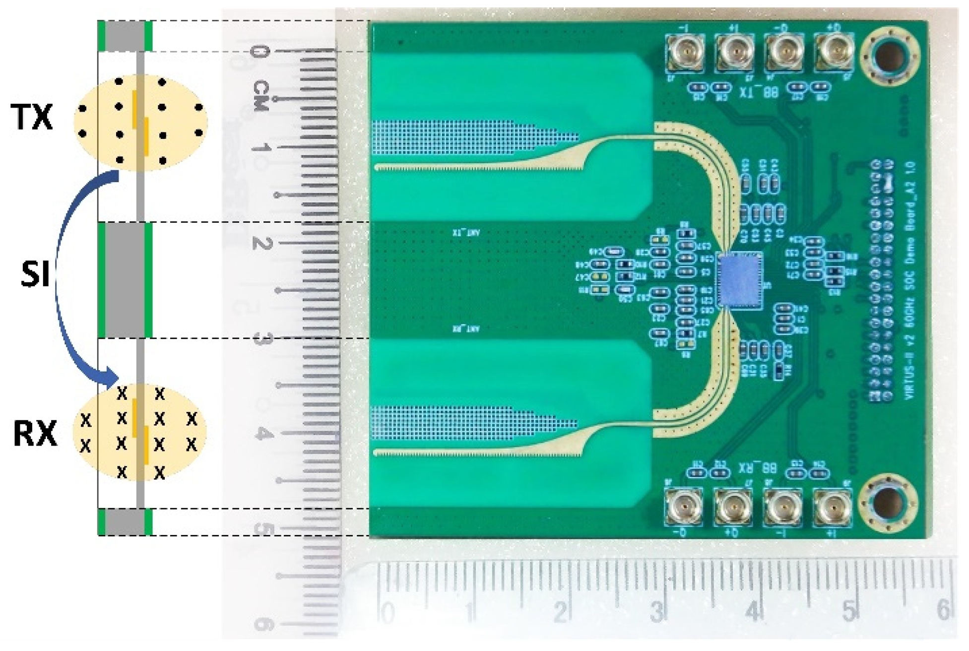
Two adjacent antipodal fermi antennas are embedded on FR4 RF PCB separately for transmitter and receiver. The antenna has a half-power beamwidth of 17◦ and 24◦ in E-plane and H-plane respectively [
28].
Figure 4 shows the top view of fabricated PCB with a pair of antennas and corresponding interconnection transmission lines. The quadrature baseband signals are placed on the sides of the PCB as shown in
Figure 4. The double row 40 pin connector is placed at the right side for power supply and control signals from the motherboard. The left cross-sectional view of the PCB with antenna beams is shown in
Figure 4 marks the thickness of different materials used in the PCB design. Two separate antennas avoid the difficulties of signal isolation within the antenna unlike the single antenna FD in [
11]. For the antenna design, a pair of conducting arms are placed symmetrically on both sides of the RO4003 substrate layer. Moreover, the whole antenna is placed on a slot of FR4 board that is much thicker than the antenna.
The narrow beam antenna is designed to deliver maximum energy in the direction of the antenna tip pointing with a small-angle coverage. The TX and RX antenna will send power in the marked direction, and the energy propagated between them is minimized. The measurement shows around 30dB drop for the energy propagation in orthogonal direction compared with the beam direction [
28]. The thick FR4 board between the two antennas also blocks the direct propagation path be-tween them to further reduce power transfer. The board-level measurement is performed to extract the energy leakage through the near-field of the antenna and the mutual coupling. Keysight PNA-N5247 network analyzer is used to analyze the board-level leakage signal across the interested band. The measurement is performed with a 5dBm input signal fed to one of the antennas, and the received signal power in the other antenna is measured. The measured S21 shows more than 80dB attenuation in the interested frequency ranges from 57GHz to 67GHz. The SI leakage in the board is lower than the noise floor, and it can be ignored.
B. Digital SI Cancellation Scheme
The SI power should be less than -67.6dBm to ensure FD operation has benefits compared to HD operation for a 3m com-munication distance. This is challenging to achieve by only RF isolation approach. This section focuses on digital SI can-cellation scheme to relax RF related leakage optimization requirement. To simplify digital SI cancellation (DSIC) scheme, only linear transformation is adopted in this work and the dominant SI leakage source considered is from PA’s output to LNA’s input. So, the transmitter signal Stx can be expressed as in (1): where, I and Q are the baseband signal, ω0 is the LO carry frequency, φtx, θtx are the phase noise and initial phase of the transmitter LO.
The transmitted RF signal Stx loopback to LNA’s input through an undesired SI leakage path and will be down- converted through the receiver chain by using the same LO ω0, but with phase noise φrx, and an initial phase θrx. The received I/Q base-band signal is captured by analog-to-digital converter (ADC) in the baseband processor. The captured baseband signal be-fore ADC can be expressed as:
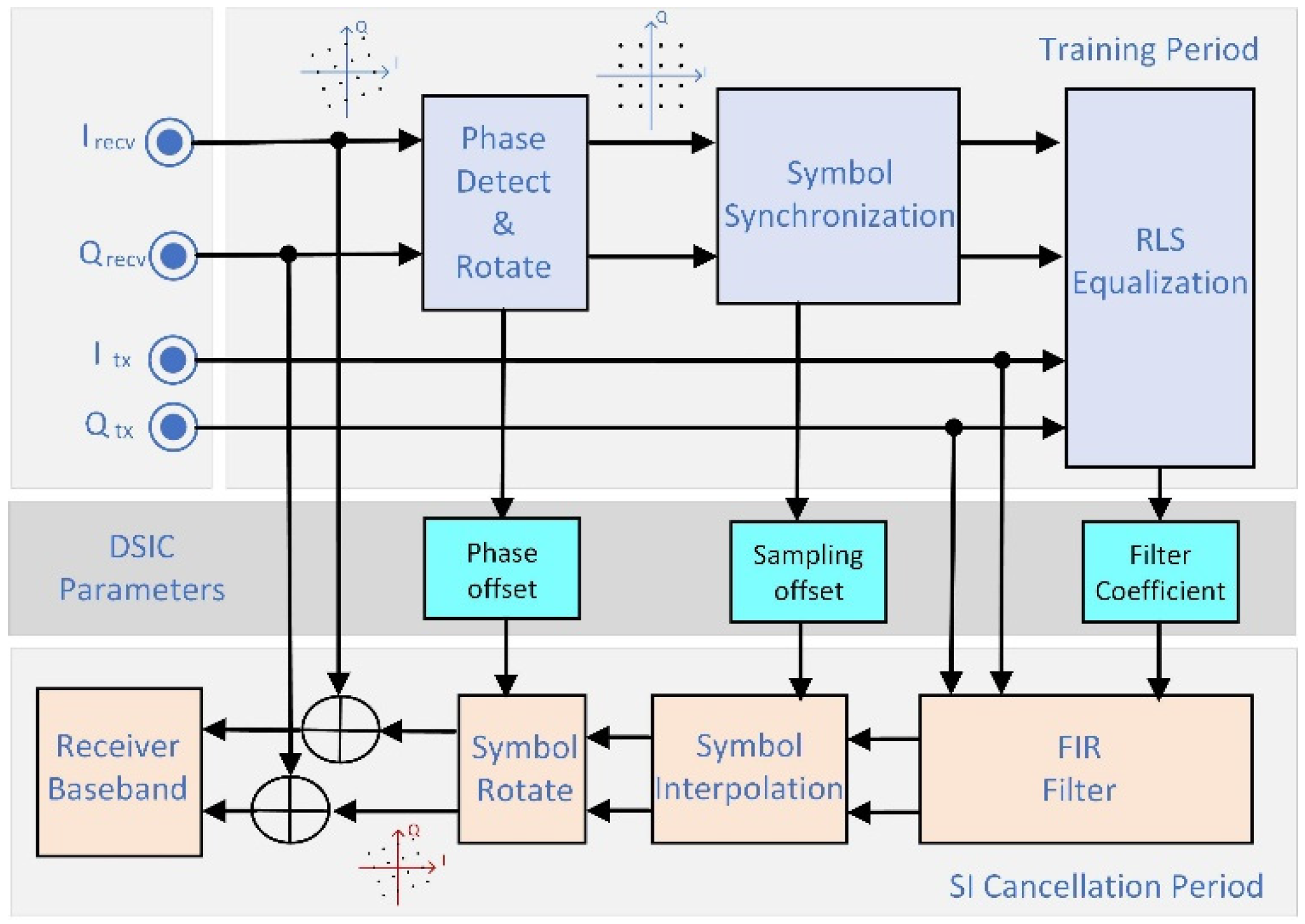
where φtrx = φtx − φrx and θtrx = θtx − θrx. It is clearly seen that SI signal is related to LO phase noise, and it is rotated de-pending on the initial phase θtxr. Equation (2) shows that the phase noise is effectively doubled as φtx and φrx is not related to each other, and there is a constant phase rotation in the received I/Q signal. At the same time, the propagation delay of the signal causes offset between sampling time of the receiver ADC to the ideal sampling time. The time-domain equaliza-tion filter is used after the phase rotation and symbol synchronization to minimize the error between the received leakage signal and the estimated value. Here, the propagation delay and channel effect of the SI leakage channel is assumed to be fixed across the time and input signals.
Figure 5 shows the block diagram of the proposed DSIC scheme. The design is im-plemented in MATLAB with four times oversampling data captured by an oscilloscope. Irecv, Qrecv are received baseband signal, and Itx, Qtx are the original signal from the transmitter. The data sequence is separated into training period and SI can-cellation period as shown in
Figure 5. During the training period, only SI leakage signal is available in the receiver chains. The IEEE 802.11ad based frame packages are used as training sequence. Firstly, the I/Q data related correlation is calcu-lated in the phase rotation module to detect the package and estimate the initial phase simultaneously. Then, the Gardner filter is used for symbol synchronization after phase rotation. It helps to correct the sampling time offset. Final-ly, a symmetrical filter with 21 multipliers is implemented as a 41 tapped finite impulse response (FIR) filter to do time-domain equalization among 10 symbols. The FIR based recursive least squares (RLS) algorithms is used as an adaptive filter to optimize the equalization filter. The FIR filter coefficients are calculated during the training period and main-tained for the SI cancellation period. A 3rd- order LaGrange interpolation module is used to regenerate the symbol data based on the estimated sampling time offset. Then, SI leakage signal is regenerated after phase rotation, and it is subtract-ed from the received baseband signal. In the proposed system, DSIC is executed in MATLAB. The transmission baseband signal Itx, Qtx must be synchronized to the received sequence again before SI cancellation runs. The evaluation of DSIC assumes that SI signal is 12dB lower than the wanted signal with a given phase rotation and sampling offset. The concept simulation is running based on the ideal test patterns with a few specified effects, including phase rotation, sampling offset, and additional Gaussian white noise. The phase noise and channel flatness degradation are not included in DSIC simulation. The simulation achieves more than 20dB SI cancellation by using a 6-bit ADC, with perfect alignment of phase and sampling time. The finer ADC resolution achieves better performance based on a 6-dB improvement per bit. However, the performance is sensitive to the symbol sampling time offset. It will drop to 5dB with the worst estimated sampling tim-ing offset. The DSIC module achieves an 8-dB SNR improvement by using the 41 tapped FIR filter with an 8 bits ADC at 4 times over-sampling with measured data. The SINR of the input signal is around 12dB and the input signal is fully occu-pied by the 10-bit ADC’s input range. Detailed information is introduced in the next section.
IV. SYSTEM MEASUREMENT
Figure 6(a) shows the evaluation platform with die photo of the fabricated transceiver chipset in
Figure 6(b). The transceiver’s die size is 4mm×5mm, including 64 ESD protected I/O pads. As shown in
Figure 6(b), the transmitter and receiver sub-systems are placed on the bottom and top side of the chip for maximum signal isolation, and the PLL is placed in between.
Figure 6(a) shows the PCB with the transceiver chip assembled on the RF board and is integrated with two on-board antennas. A moth-erboard powered with an NXP 8-bit MC9S08JM60 MCU controls the RF frontend’s working conditions and monitors its power consumption. A Windows-based software is used to configure the working condition of the RF chipset through a GUI interface. A mini-USB port works as both the control bus and the power supply of the platform. There are two quadra-ture differential baseband interfaces matched to 100Ω impedance and are available on the RF board as transmitter input and receiver output. A 108MHz TCXO crystal board works as a reference for the RF platform.
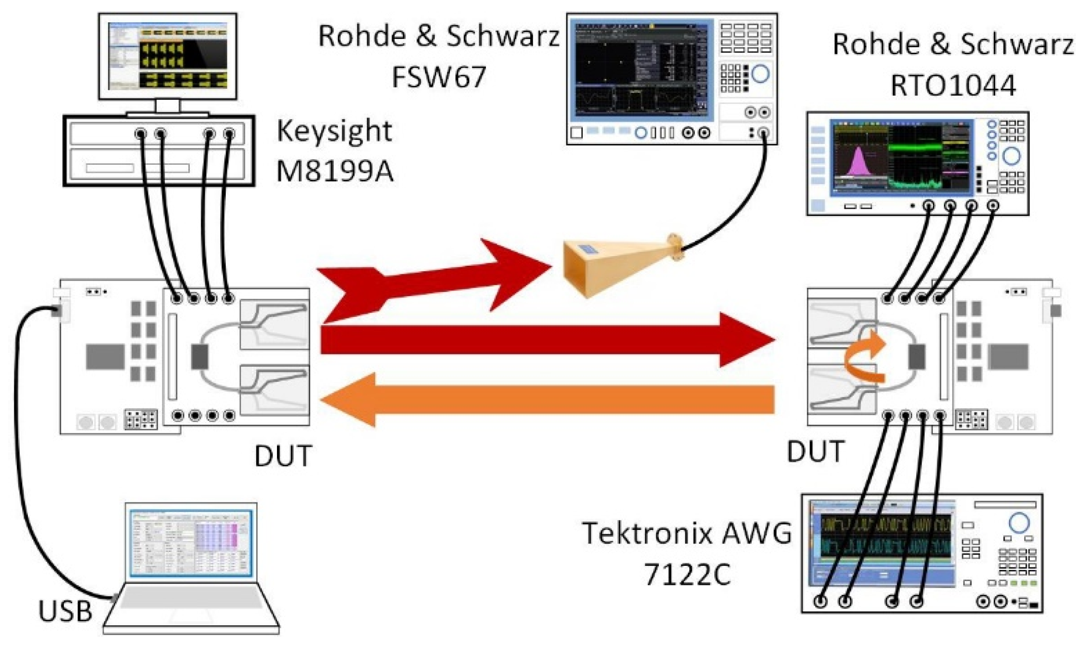
Figure 7 shows the measurement setup of the transceiver system. One set of DUT is configured as the transmitter. Keysight M8199 arbitrary waveform generator (AWG) with corresponding software features (81199A) is used to generate a base-band test pattern. A horn antenna is connected to Rohde & Schwarz FSW67 spectrum analyzer to check the transmitter power. The single tone baseband signal is used to measure the maximum output power of PA and channel flatness over the specified frequency band. The power plot is calculated based on the measured power amending with the estimated setup losses.
Another set of DUT is configured in the full-duplex mode to down-convert the RF signal transmitted by the first set of DUT with its own local leakage. The single tone signal helps analyze the relationship between the received signal and local SI from the transmitter. Furthermore, 802.11ad based package frame support measures the signal quality through the demodu-lated EVM. A Tektronix AWG 7122C is used as the second baseband source. The AWG has dual channel 12GSym/s digi-tal-to-analog converters (DACs) to support the 802.11ad standard. A Rohde & Schwarz RTO 1044 oscilloscope captures the baseband signal for further analysis and calculates the EVM. It captures the received baseband data at 10GSyms/s. MATLAB is used to resample the data to 4 times oversampling and remove the out-band noise as well. The virtual storage extended (VSE) software with 802.11ad features from Rohde & Schwarz was used to demodulate the received baseband quadrature signal and plot the EVM. For the full-duplex mode, the captured data is filtered by a digital filter in MATLAB to reduce the SI signal power through the DSIC module. The generated data is demodulated and analyzed by Keysight VSA software.
A. Transmitter Power
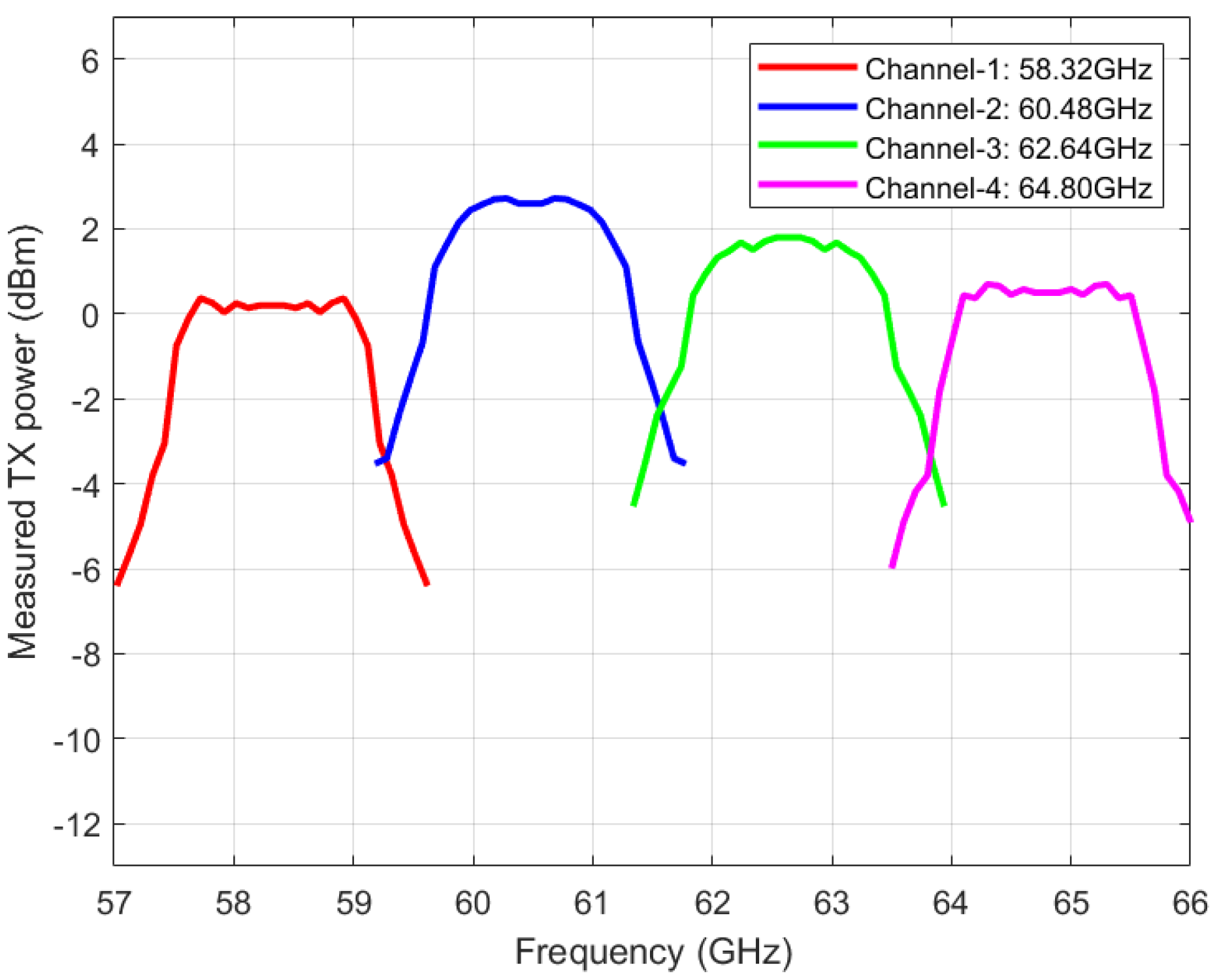
The transmitter power is measured by using a single tone quadrature signal, varying frequencies from 100MHz to 1.3GHz with a 100MHz frequency step. The measured power is plotted based on four-channel modulation and mirrors for the same frequency offset, as shown in
Figure 8. The measurement is taken at a 1m distance with an additional 3dB amplifier GPA between the receiver horn antenna and the FSW67 spectrum analyzer. An additional 60GHz amplifier is added as the received signal power is too low for FSW67 to demodulate. Based on the setup, considering the free-space link loss Gpl to be 68dB, the gain of onboard transmitter antenna Gtx and horn antenna Grx are 12dBi and 17dBi, respectively. Also, the total loss for 60GHz cables and adaptors Gcable is 8.7dB. The transceiver output power is 16.7dB higher than the directly measured value as es-timated in (3).
Figure 8 plots the transmission power of the transceiver chip based on the measurement results.
It clearly shows that channel 2 has the highest output power compared with other channels, and all four channels have less than 1-dB channel flatness within the 1.76GHz bandwidth. The saturated output power for the transceiver is around 2.7dBm. The power significantly drops for out- band signals because the baseband DVGA in the transmitter chain filters the unwanted baseband to meet the spectrum mark requirements.
B. HD Link Measurement
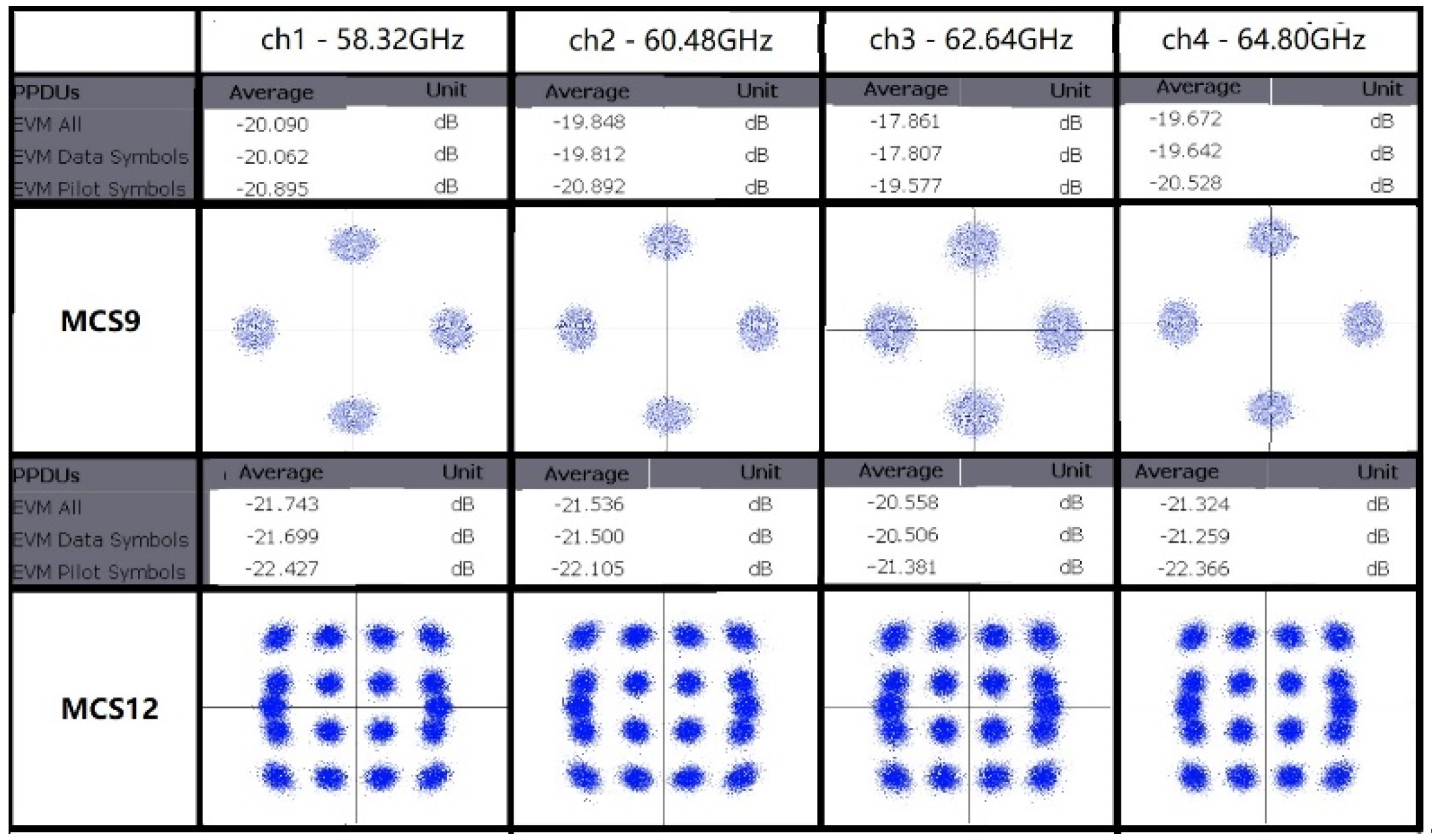
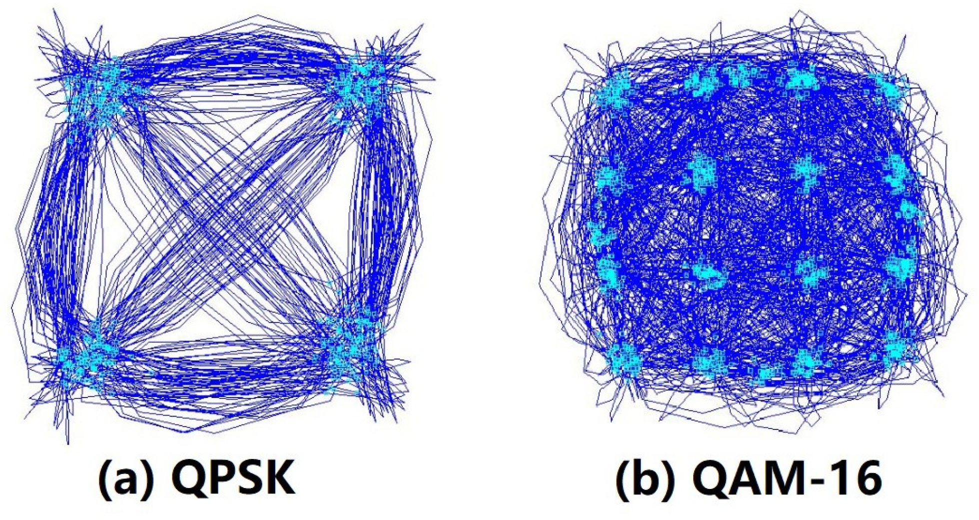
The half-duplex 802.11ad modulation is measured at 1.5m communication distance for all the four channels and is shown in
Figure 9. It is defined based on the measured maximum output power, with 6-dB peak-to-average power ratio (PAPR) linear protection range for the modulated signals. In this HD measurement, the transmission power for MCS9 and MCS12 are set at 3dB and 6dB, respectively, lower than the maximum output power to have good linearity of the modulated signal. As shown in
Figure 9, the measured EVM is very close to -21dB for all channels, which is the basic EVM requirements for MCS12 of IEEE 802.11ad standard. In the constellation diagram, the measured average EVM across the 4 channels for 1,000 symbols under MCS12 are -21.7dB, -21.5dB, -20.5dB and -21.3dB, respectively for 16-QAM modulated data symbols, and -22.4dB, -22.1dB, -21.4dB and -22.4dB, respectively for pilot symbols modulated using π/2-BPSK. The pro-posed transceiver fulfills the EVM requirement MCS12 for channels 1, 2 and 4, and 0.5-dB margin for channel 3. The QPSK modulated signal is plotted in the same figure, which is better than the EVM specification requirements of -16 dB defined in MCS9.1.
The MCS12.3 to 12.6 are added to the WiFi standard in 2016 to support higher data rate by introducing 64-QAM support in a single carry modulation.
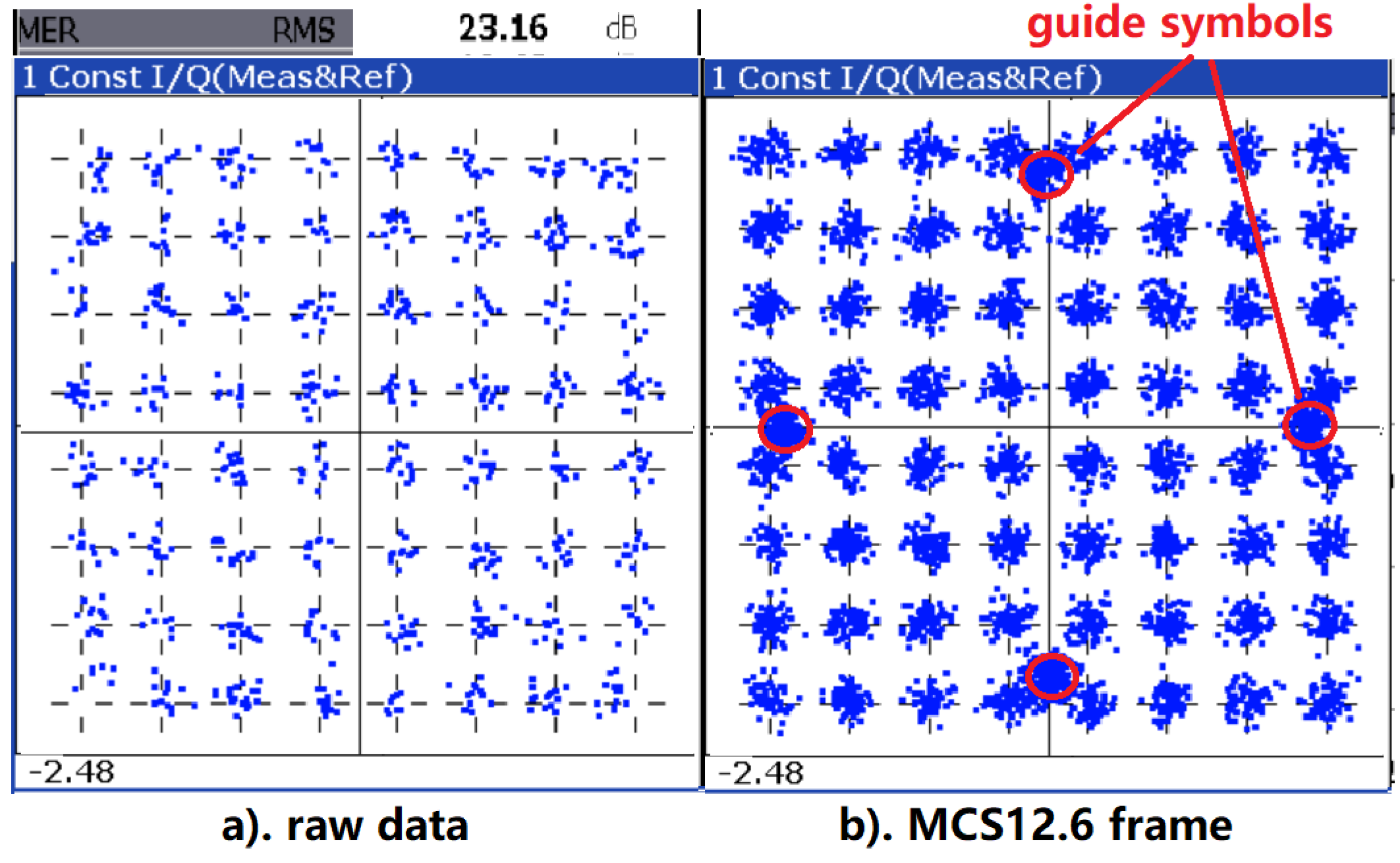
Figure 10 shows the 64-QAM modulated signal with symbol rate at 1.5GSym/s, and raw data rate of 9Gbps.
Figure 10(a) shows the raw data demodulation without frame header, and
Figure 10(b) is the constellation plot for an MCS12.6 frame package. The reported EVM value is 23.16dB for raw data. Other than the frame-based measurement for 802.11ad standard, the raw data in
Figure 10(a) without package header may degrade the measured EVM value because of poor synchronization and equalization.
Figure 10(b) captured a frame package with π/2-BPSK modulated header and guide symbols. It shows better in symbol gathering, especially for high-power symbols located at the constellation diagram cor-ner. However, the EVM result here is 21.88dB as the VSE software cannot separate the guide symbols from data symbols correctly in the current release.
The power consumption of the transmitter and receiver is 194.1mW and 231.4mW, respectively. Here, the power consump-tion is measured at 1.5m communication distance using MCS12 of 802.11ad standard. The communication distance can be further increased for constant amplitude modulation, such as BPSK and QPSK, with PA’s saturated output. The maximum transmitter power consumption is 312.7mW when using a 2.4V power supply.
C. Frequency Division Duplex Measurement
For the FDD measurement, the communication distance is set to 0.8m as the measured transmitted power drops around 6dB for FDD operation mode compared to HD. The reason for such power drop is the output power of LO signal feed to 12GHz I/Q mixer and 24GHz harmonic up-mixer are dropped when the loading network changes to drive both the transmitter and receiver chains. The performance measurement is performed with four different test conditions: firstly, signal is transmitted from channel 2, and received at channels 1 and 3, and secondly, data is sent from channels 1 and 3, while receiving them at channel 2. For all the measurements, the received baseband output signal ’I’ is taken by oscilloscope and then demodu-lated directly using VSE software. Here, the Rohde & Schwarz RTO 1044 is used as a baseband oscilloscope that samples the received signal at 10GSym/s. The SI signal here is removed by the bandpass digital filter in VSE software directly.
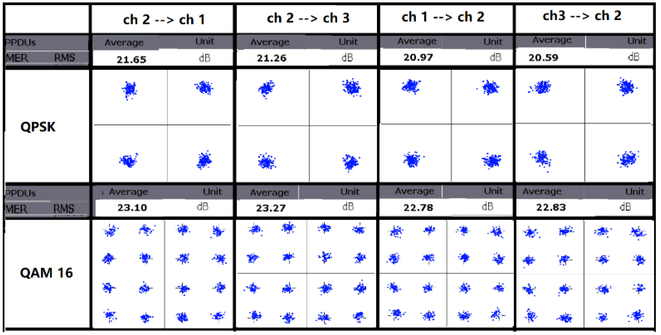
Figure 11 shows the measured constellation diagram with average EVM results. The performance is better than HD measurement, and it meets the EVM requirement of MCS12.2.
Such EVM improvement occurs due to three reasons. Firstly, the reduced communication distance increases the received signal power by 5.5dB. In other words, the power drop of the transmitter in FDD mode is compensated by the communica-tion distance. Secondly, the smaller input signals improve the linearity of the VGA, mixer, and PA. Finally, the high resolu-tion, high sampling rate of the oscilloscope completely removed the SI noise in the digital baseband processor. The meas-ured average EVM across the 4 test conditions for 500 symbols under 16-QAM are -23.2dB, -23.27dB, -22.78dB and -22.83dB respectively, and -21.65dB, -21.26dB, -20.97dB and -20.59dB respectively for QPSK data symbols
D. Full-Duplex Measurement
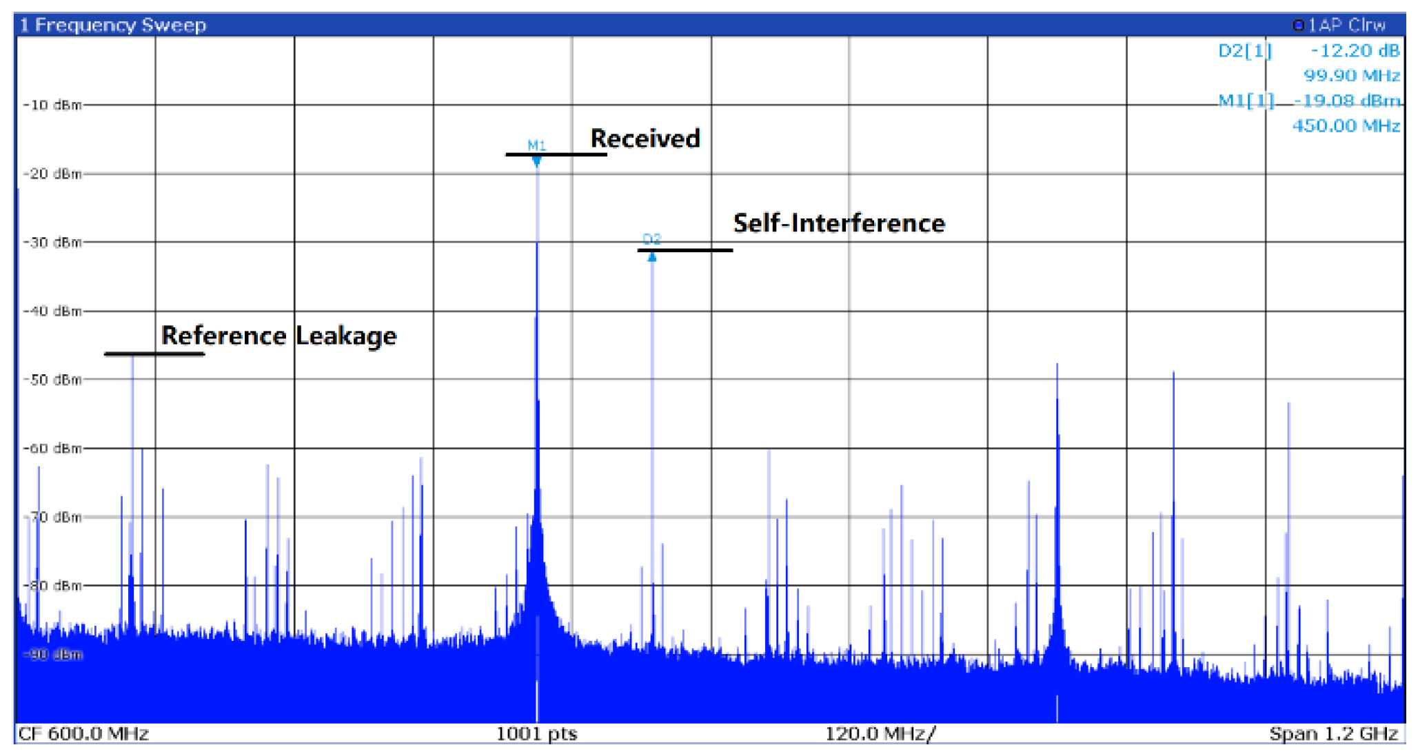
Figure 12 shows the single tone signal’s power spectrum received together with the local SI at 0.8m. The measured transmis-sion power is -3dBm. The 450MHz is the received signal from the antenna, and the 550MHz is the SI from the local trans-mitter. Here, both transmitters are configured at the same condition with similar PA output power, and both transmitter and receiver are operated on channel 2. The transmission loss here is 42dB as calculated in (3), where the antenna gains for the transmitter Gtx and receiver Grx are all 12dBi.
The received power achieves a maximum peak-to-peak output voltage Vpp of DVGA. The measured receiver chain gain Grec here is 26.08dB as calculated in (4), where Prec−out is the output power of receiver chain and Prec−in is the input power to the LNA.
As plotted in
Figure 12, the estimated isolation between the output of PA to the input of LNA is 54.2dB based on the measured SI power level of -31.28dBm, as shown in (5), when the Prec−in−SI is the input SI power at receive chain, PPA−out is the output power from PA. The Prec−in−SI is calculated based on the output power of the receiver chain and the gain of the chain. The maximum isolation for FD mode can be achieved around 35 dB when setting the programmable amplifier (DVGA and IFA) to minimal gain condition. However, the communication distance must reduce to 0.45m to compensate for the gain drops here.
For the modulated signal measurement, the RF isolation is around 30dB as 5dB gain is set at receiver DVGA to get enough baseband signal amplitude.
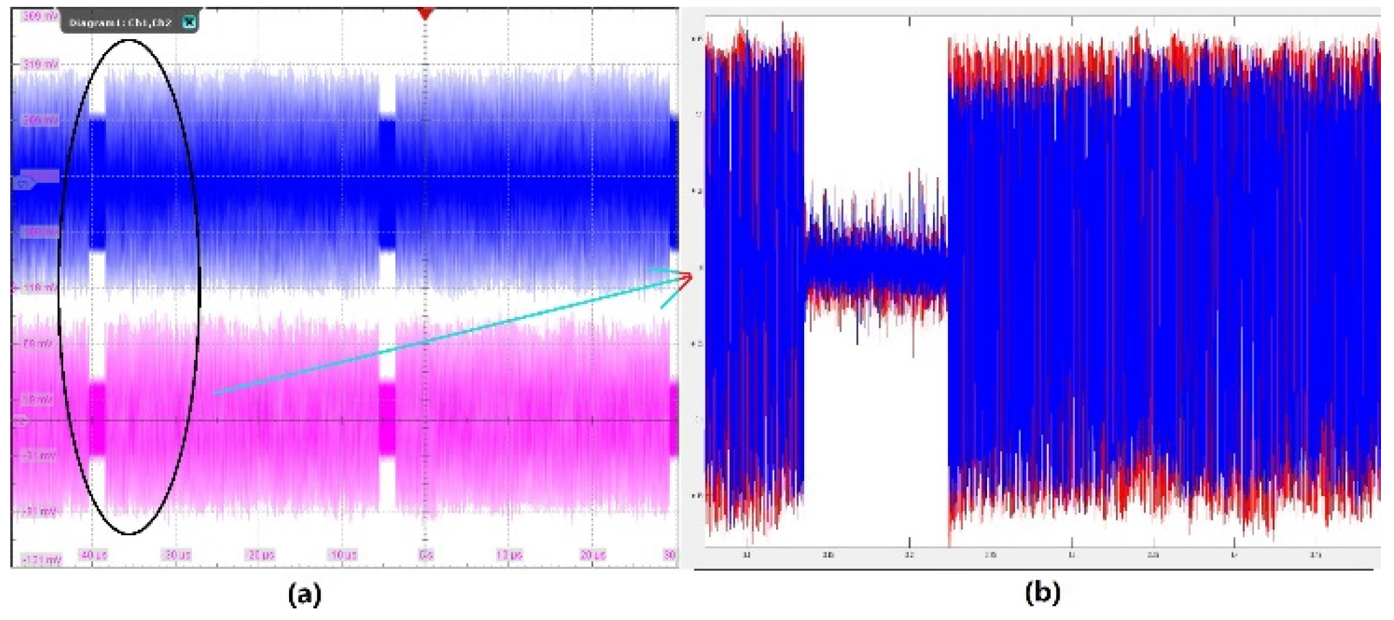
Figure 13 shows the time domain signal before and after DSIC processing. There two frame pack-ages available with 2µs gap between them are captured in
Figure 13(a). The SI signal is available all the time, and it can be observed easily during the 2µs package gap. The I and Q signals are captured by oscilloscope in channels 1 and 2, shown in
Figure 13(a).
Figure 13(b) plots the received package data after DSIC module. Here, the Rohde & Schwarz RTO 1044 oscillo-scope captured data at 10GSym/s, with 8-bits valuable ADC output. The symbol rate of the test sequence is 1GSym/s for both transmitters. The captured data is resampled at 4GHz, and out-band noise is removed before sending to the DSIC.
The dominant SI signal in the system comes from the 60GHz domain before LNA input. To measure the isolation between transmitter to receiver chain, the gain of receiver IFA is set to minimal, and the DVGA gain to 5dB. The output data from DSIC is demodulated by Keysight 89600 VSA as shown in
Figure 14. The reported EVM for QPSK and 16-QAM is -17.05dB and -17.8dB, respectively. Here, the 16-QAM based EVM is worse than the actual value, as 1/8 of symbols are pilot and modulated by π/2-BPSK. It is not mapping correctly. Assuming all the pilot symbols have a similar vector error as the data symbols, the amended EVM for all symbols should be -18.7dB in 16-QAM. As the VSA software cannot decode the origi-nal package before DSIC, we assume the EVM is the same as the received SINR, which is 12dB as shown in
Figure 12. Hence, the MATLAB based DSIC in this measurement achieved 6.7dB EVM improvement.
The above measurement covers three different working modes, HD, FDD, and FD. Firstly, based on the measurement results, the design satisfies the specification to support 802.11ad communication standard at 1.5m up to MCS12. The transceiver covers the design specifications of 3m for MCS9, as the power can further increase, and the PA linearity is not an issue for QPSK modulated signal. Secondly, the FDD and FD measurements are done at 0.8m communication distance, as the maximum transmitter power is 6dB lower than that in HD. Thirdly, the FD is measured at 0.8m to fulfill the 12-dB SINR before the DSIC processing. The FD baseband data cannot be demodulated directly by using Keysight VSA software without DSIC. The MATLAB based DSIC is introduced to suppress SI, and it achieves 6.2-dB SINR gain.
Table 2 summarizes the measured performance with the state-of-the-art. As can be seen in
Table 2, this work realizes the fully integrated low-power 802.11ad compatible RF transceiver with FDD and FD support, which simultaneously achieves 7.04Gbps and 4Gbps for both transmitter and receiver in FDD and FD mode, respectively.The above measurement covers three different working modes, HD, FDD, and FD. Firstly, based on the measurement re-sults, the design satisfies the specification to support 802.11ad communication standard at 1.5m up to MCS12. The trans-ceiver covers the design specifications of 3m for MCS9, as the power can further increase, and the PA linearity is not an issue for QPSK modulated signal. Secondly, the FDD and FD measurements are done at 0.8m communication distance, as the maximum transmitter power is 6dB lower than that in HD. Thirdly, the FD is measured at 0.8m to fulfill the 12-dB SINR before the DSIC processing. The FD baseband data cannot be demodulated directly by using Keysight VSA software with-out DSIC. The MATLAB based DSIC is introduced to suppress SI, and it achieves 6.2-dB SINR gain.
Table 2 summarizes the measured performance with the state-of-the-art. As can be seen in
Table 2, this work realizes the fully integrated low-power 802.11ad compatible RF transceiver with FDD and FD support, which simultaneously achieves 7.04Gbps and 4Gbps for both transmitter and receiver in FDD and FD mode, respectively.
V. CONCLUSIONS
This paper presents a low power 60GHz BiCMOS transceiver fully compatible with IEEE 802.11ad wireless standard. In contrast to the traditional mode, the proposed transceiver allows FDD operation with -22.78dB and -20.97dB, and FD op-eration with -18.7dB and -17.05dB EVM at 0.8m communication distance for 16-QAM and QPSK, respectively. The max-imum data rate is 7.04Gb/s for both the transmitter and receiver. The FD operation mode in the proposed system works only in π/2 BPSK without a DSIC and works in 16-QAM with DSIC. Moreover, with a 4-GHz, 3-dB bandwidth of I/Q base-band DVGA, together with 6-GHz, 3-dB bandwidth of IF amplifier, the transceiver can also support 2-channel bonding re-ceiver operation defined in IEEE 802.11ay with a doubled data rate of 14.08Gb/s.
References
- J. Pang and K. K. Tokgoz, “A 28.16-Gb/s area-efficient 60-GHz CMOS bidirectional transceiver for IEEE 802.11ay,” IEEE Trans. Microw. Theory Techn, vol. 68, no. 1, pp. 252–263, 2020. [CrossRef]
- J. Pang, S. Maki et al., “A 50.1-Gb/s 60-GHz CMOS transceiver for IEEE 802.11ay with calibration of LO feedthrough and I/Q imbalance,” IEEE J. Solid-State Circuit, vol. 54, no. 5, pp. 1375–1390, 2019. [CrossRef]
- C. W. Byeon, K. C. Eun, and C. S. Park, “A 2.65-pJ/bit 12.5-Gb/s 60-GHz OOK CMOS transmitter and receiver for proximity communications,” IEEE Trans. Microw. Theory Techn, vol. 68, no. 7, pp. 2902–2910, 2020. [CrossRef]
- U. Kodak, B. Rupakula et al., “60-GHz 64- and 256-element dual-polarized dual-beam wafer-scale phased- array transceivers with reticle-to-reticle stitching,” IEEE Trans. Microw. Theory Techn, vol. 68, no. 7, pp. 2745– 2767, 2020. [CrossRef]
- K. E. Kolodziej, B. T. Perry et al., “In-band full-duplex technology: Techniques and systems survey,” IEEE Trans. on Microw. Theory and Techn, vol. 67, no. 7, pp. 3025–3041, 2019. [CrossRef]
- Z. Wei, X. Zhu et al., “Full-duplex versus half-duplex amplify-and-forward relaying: Which is more energy efficient in 60-GHz dual-hop indoor wireless systems?” IEEE J. Select. Areas Commun., vol. 33, no. 12, pp. 2936–2947, 2015. [CrossRef]
- G. Liu, F. R. Yu et al., “In-band full-duplex relaying: A survey, research issues and challenges,” IEEE Commun. Surveys Tuts., vol. 17, no. 2, pp. 500–524, 2015. [CrossRef]
- T. Dinc, A. Chakrabarti et al., “A 60GHz CMOS full-duplex transceiver and link with polarization-based antenna and RF cancellation,” IEEE J. Solid-State Circuit, vol. 51, no. 5, pp. 1125–1140, 2016. [CrossRef]
- S. Khaledian, F. Farzami et al., “Inherent self-interference cancellation for in-band full-duplex single- antenna systems,” IEEE Trans. on Microw. Theory and Techn, vol. 66, no. 6, pp. 2842–2850, 2018. [CrossRef]
- A. Vosoogh, M. Sharifi Sorkherizi et al., “Compact integrated full-duplex gap waveguide-based radio frontend for multi-Gbit/s point-to-point backhaul links at E-band,” IEEE Trans. on Microw. Theory and Techn, vol. 67, no. 9, pp. 3783–3797, 2019. [CrossRef]
- T. Chi, J. S. Park et al., “A millimeter-wave polarization-division-duplex transceiver frontend with an on-chip multi-feed self-interference-canceling antenna and an all-passive reconfigurable canceller,” IEEE J. Solid-State Circuit, vol. 53, no. 12, pp. 3628–3639, 2018. [CrossRef]
- “IEEE standard for information technology: Telecommunications and information exchange between systems local and metropolitan area networks—specific requirements-Part 11: Wireless LAN medium access control (MAC) and physical layer (PHY) specifications,” IEEE Std 802.11-2016, pp. 2408, 2016.
- S.-K. Yong, P. Xia et al., “60GHz channel characterizations and modeling,” in 60GHz Technology for Gbps WLAN and WPAN. Wiley, ch. 2, pp. 17–61. [CrossRef]
- P. F. M. Smulders, “Statistical characterization of 60GHz indoor radio channels,” IEEE Trans. Antennas and Propag., vol. 57, no. 10, pp. 2820–2829, 2009. [CrossRef]
- Q. Zou, K. S. Yeo et al., “A fully symmetrical 60GHz transceiver architecture for IEEE 802.15.3c application,” in IEEE Int. Conf. on Solid-State and Integrated Circuit Tech., 2010, pp. 713–715. [CrossRef]
- Kaixue Ma, S. Mou et al., “An integrated 60GHz low power two-chip wireless system based on IEEE 802.11ad standard,” in IEEE MTT-S Int. Microw. Symp. Dig., 2014, pp. 1–4. [CrossRef]
- Y. Wang, K. Ma, and K. S. Yeo, “A hybrid CMOS clock divider for PLL of 60GHz transceiver,” in URSI General Assembly and Sci. Symp. (URSI GASS), 2014, pp. 1–4. [CrossRef]
- T. B. Kumar, K. Ma et al., “A 7.9-mw 5.6-ghz digitally controlled variable gain amplifier with linearization,” IEEE Trans. Microw. Theory Techn, vol. 60, no. 11, pp. 3482–3490, 2012. [CrossRef]
- T. Kumar, K. Ma et al., “A 35-mW 30-dB gain control range current mode linear-in-decibel programmable gain amplifier with bandwidth enhancement,” IEEE Trans. Microw. Theory Techn, vol. 62, no. 12, pp. 3465–3475, 2014. [CrossRef]
- D. van den Broek, E. A. M. Klumperink et al., “An in-band full-duplex radio receiver with a passive vector modulator down mixer for self-interference cancellation,” IEEE J. Solid-State Circuits, vol. 50, no. 12, pp. 3003– 3014, 2015. [CrossRef]
- A. Kiayani, M. Z. Waheed et al., “Adaptive nonlinear RF cancellation for improved isolation in simultaneous transmit-receive systems,” IEEE Trans. on Microw. Theory and Techn, vol. 66, no. 5, pp. 2299–2312, 2018. [CrossRef]
- E. Ahmed and A. M. Eltawil, “All-digital self-interference cancellation technique for full-duplex systems,” IEEE Trans. on Wireless Commun., vol. 14, no. 7, pp. 3519–3532, 2015. [CrossRef]
- N. Ginzberg, D. Regev et al., “A full-duplex quadrature balanced RF frontend with digital pre-PA self-interference cancellation,” IEEE Trans. on Microw. Theory and Techn, vol. 67, no. 12, pp. 5257–5267, 2019. [CrossRef]
- S. Mondal and J. Paramesh, “Power-efficient design techniques for mm-wave hybrid/digital FDD/full-duplex MIMO transceivers,” IEEE J. Solid-State Circuit, vol. 55, no. 8, pp. 2011–2026, 2020. [CrossRef]
- D. Korpi and T. Riihonen, “Full-duplex transceiver system calculations: Analysis of ADC and linearity challenges,” IEEE Trans. Wireless Commun., vol. 13, no. 7, pp. 3821–3836, 2014. [CrossRef]
- Z. Zhang, K. Long, et al., “Full-duplex wireless communications: Challenges, solutions, and future research directions,” Proceedings of the IEEE, vol. 104, no. 7, pp. 1369–1409, 2016. [CrossRef]
- K. Ma, Shouxian Mou et al., “A miniaturized 28mW 60GHz differential quadrature sub-harmonic QPSK modulator in 0.18µm SiGe BiCMOS,” in IEEE MTT-S Int. Microw. Symp. Dig., 2014, pp. 1–4. [CrossRef]
- M. Sun, Xianming Qing et al., “60-GHz antipodal Fermi antenna on PCB,” in 5th Eur. Conf. on Antennas and Propag. (EUCAP), 2011, pp. 3109–3112.
- N. Mahalingam, Y. Wang et al., “A 24GHz low power low phase noise dual-mode phase locked loop frequency synthesizer for 60 GHz applications,” in IEEE MTT-S Int. Microw. Symp. Dig., 2014, pp. 1–4. [CrossRef]
- K. Wang, K. Ma et al., “Design consideration for 60GHz SiGe power amplifier with ESD protection,” in Int. SoC Design Conf., 2011, pp. 5–8. [CrossRef]
- N. Mahalingam, Y. Wang et al., “A 30-GHz power-efficient PLL frequency synthesizer for 60-GHz applications,” IEEE Trans. Microw. Theory Techn, vol. 65, no. 11, pp. 4165–4175, 2017. [CrossRef]
- P. Yeh, H. Chiou et al., “An experimental study on high-frequency substrate noise isolation in BiCMOS technology,” IEEE Electron Device Lett., vol. 29, no. 3, pp. 255–258, 2008. [CrossRef]
|
Disclaimer/Publisher’s Note: The statements, opinions and data contained in all publications are solely those of the individual author(s) and contributor(s) and not of MDPI and/or the editor(s). MDPI and/or the editor(s) disclaim responsibility for any injury to people or property resulting from any ideas, methods, instructions or products referred to in the content. |
© 2023 by the authors. Licensee MDPI, Basel, Switzerland. This article is an open access article distributed under the terms and conditions of the Creative Commons Attribution (CC BY) license (http://creativecommons.org/licenses/by/4.0/).
