1. Introduction
Beam scanning antennas play a key role in 5G communication system to attain the desired output. The use of beamforming feeding networks (BFNs) is an essential technique to obtain high directivity in a particular direction and improve the connection quality as well as coverage for the 5G system [
1]. The function of BFNs is to adjust the phase and amplitude of feeding signals for phased array antenna systems [
2]. Butler-matrix (BM) is one of the most common BFNs of 5G systems owing to distinctive features such as simplicity, lower-cost, and easy fabrication process. In addition, BM doesn't need external biasing in its operation. Besides, BM operates as a reciprocal feeding system for transmitting and receiving signals in phased array antenna systems. The building block of the BM is the BLC, which can be utilized as a modulator, mixer, and phase shifter, as well as its basic function as part of a feeding network of phased array antenna system [
1]. Therefore, this work focuses on the design of a compact BLC with enhanced bandwidth. As illustrated in
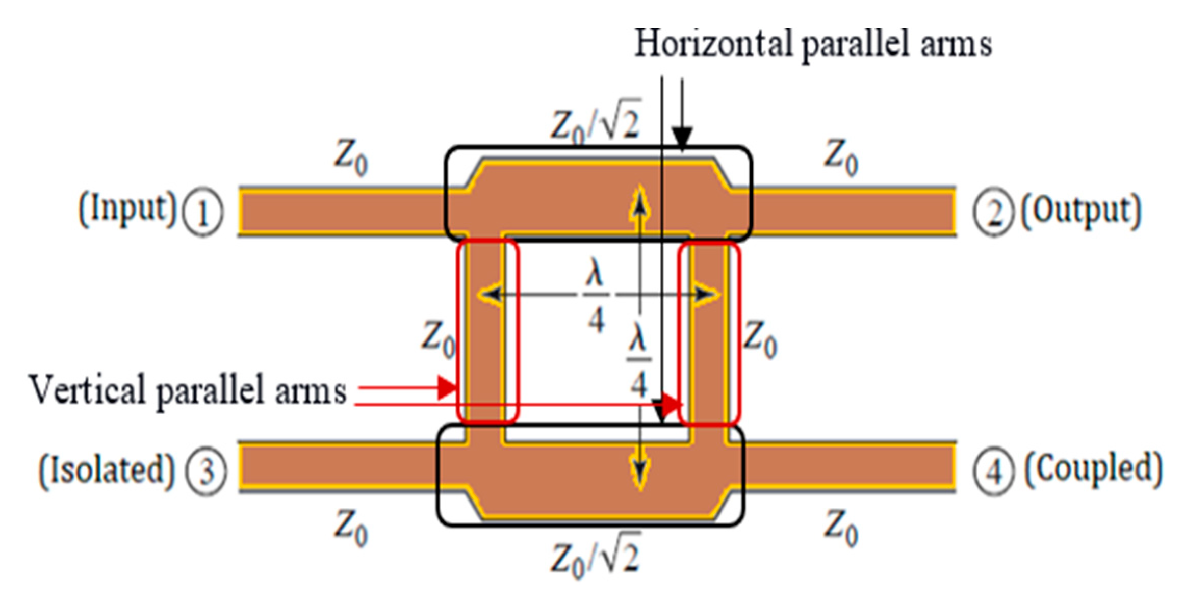
Figure 1, a BLC consists of four transmission lines grouped into two pairs, with each pair consisting of parallel horizontal and vertical lines. The characteristics impedance of the horizontal lines is Z
o/√2 while for the vertical counterparts it is Z
o, where Z
o represents the characteristics impedance of the microstrip transmission line (MSTL). Each of the four transmission lines (TL) has a length of λ
g/4, where λ
g is the guided wavelength. Thereby the dimensions of the BLC are primarily based on the operating frequency, thus in low-frequency the BLC extend over a large area of the host device board, and hence lead to an increased size [
3]. Another inherent issue with a conventional BLC is the limited bandwidth characteristics of no more than 50%, which restrict their applications and would require a large multi-sections circuit to gain wideband characteristics, which in turn increases the circuit’s area [
4].
Many efforts have been reported that address the above limitations. For example, the coupled line unit cells concept was introduced in [
3] to create a dual composite Right/Left-handed (D-CR/LH) unit cell, which results in a design that has a miniaturized area of ~ 52% of that of a conventional BLC at 1.8GHz with a relative bandwidth of 18 %. T-shaped slots and open stubs were employed in the horizontal and vertical arms of the BLC, resulting in a 30% bandwidth improvement and a 12.3% size reduction [
4].
In another study, a double-layer board with slow-wave microstrip transmission lines and blind vias was used to achieve a 43% size reduction compared to a conventional design at the same resonant frequency. However, the increased number of vias led to higher insertion losses and design complexity [
5]. A Koch fractal-shape BLC of various iterations was suggested in [
6], where the sample was designed to operate at 2.4GHz and offered a size reduction of ~81% in combination of a relative bandwidth of 33%.
In [
7], open-ended stubs and transmission line meandering with a stepped impedance approach have been proposed with a size reduction of ~61% and 50% compared to a conventional BLC, respectively. However, the narrow bandwidth of ~130 MHz represents a key limitation. A flexible coupler using a Teslin paper substrate was reported [
8]. It replaced the conventional quarter-wavelength transmission lines with a collective of shunt open-stubs, series transmission lines, and meandered lines, resulting in a compact design with a surface area of 0.04
, and a 68% fractional bandwidth. Using a dual microstrip transmission line, the BLC size was reduced by 32% with a fractional bandwidth of 60% [
9]. However, this approach had poor return losses over the operating bandwidth. To improve matching, T-shaped transmission lines were used, reducing fractional bandwidth and size to 50% and 44%, respectively. A compact BLC class introduced a prototype using open-circuited stubs to replace traditional quarter-wavelength transmission lines [
10], resulting in a ~55.6% size reduction and achieving 11% and 50% fractional bandwidth for narrowband and wideband modes of operation, respectively.
In [
11], a new configuration, BLC, is presented. The design applies two types of trapezoid-shaped resonators on the arms of the BLC to configure a wideband branch-line coupler. The proposed design has achieved a size reduction of 79% compared to conventional couplers. In addition, it offered a fractional bandwidth of 22.2%. [
12] used artificial transmission lines (ATL) for miniaturization. They replaced conventional transmission lines with right-handed transmission lines (RHTL) and constructed the branch-line coupler sides using cascaded T-Net RHTLs instead of quarter-wavelength transmission lines. This design achieved a 50% size reduction compared to the conventional BLC and a 33.3% fractional bandwidth (2.0–2.8 GHz). A simple method was used to improve bandwidth in [
13]. By adding a single transmission line element to a conventional coupler, they increased bandwidth by approximately 25%. However, the proposed structure is larger at 25.7×22.8mm compared to the conventional coupler's 21.5×20.7mm.
Triangular and trapezoidal resonators were added to the coupler for miniaturization and harmonic suppression [
14]. The design achieved an 84% size reduction and wide harmonic suppression. However, it has a complex structure with a low-frequency band around 200MHz, representing a 26% fractional bandwidth (FBW).
The majority of the aforementioned prototypes were based on composite Right/Left-handed structures to create the branch lines, which might result in unfavorable characteristics that are associated with miniaturization such as shallow return losses for input ports, poorly isolated ports, and narrow bandwidth in some cases [
3,
4,
6,
8]. In addition, the structures of Right/Left-handed transmission line probably increase the structure’s complexity, which results in a challenging practical realization despite the overall size reduction.
In this study, a quasi-twisted shape branch line coupler is proposed, which is the longitudinal bisection of the conventional BLC into two sections and twisting each over the other. The structure is designed based on the microstrip double-layered TL (MDL-TL). The input/output transmission lines and horizontal arms of the BLC are built based on Z-shape meandered section with round blend edges, while λg/4 vertical arms of BLC are adopted for the slow wave structure. The MDL-TLs are placed on two layers and were connected using four conductive vias. A common ground plane is placed between the layers of the MDL-TLs, which incorporates circular slots around the vias to avoid shorting them to the common ground plane. The described configuration reduced the size of the conventional BLC by 49.9 % and improved the relative bandwidth to 75.8%. The novel design is modelled and simulated using Computer Simulation Technology (CST) microwave studio and then fabricated and tested on a low-cost FR-4 substrate material demonstrating promising S-parameter results.
The paper is organized as follows:
Section 2 explains the theoretical analysis and design procedures of developing a wideband MDL-TL and comparing the achieved performance with that of a conventional microstrip line;
Section 3 presents the analysis and design of a branch line coupler based on MDL-TL. Finally,
Section 4 presents the simulated and measured results demonstrating the novel BLC performance.
3. Branch Linee Coupler’s Design
3.1. Conventional Branch Line Coupler
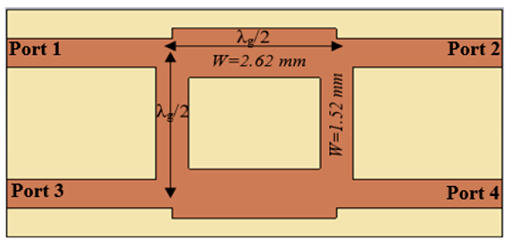
Figure 6 shows a 10 mm × 23 mm conventional BLC designed at 6GHz on an FR4 substrate with a thickness of 0.8 mm and dielectric constant (εr) of 4.4 with a loss tangent of 0.025, the same substrate specification as the proposed BLC for effective comparison. The 50 Ω microstrip line sections for ports 1,2,3, and 4 are designed with a width of 1.52 mm and the λ
g/4 sections of the coupler, of impedance Z
0/√2 (35.35 Ω) are of a microstrip line with a width of 2.62 mm, as shown in
Figure 6.
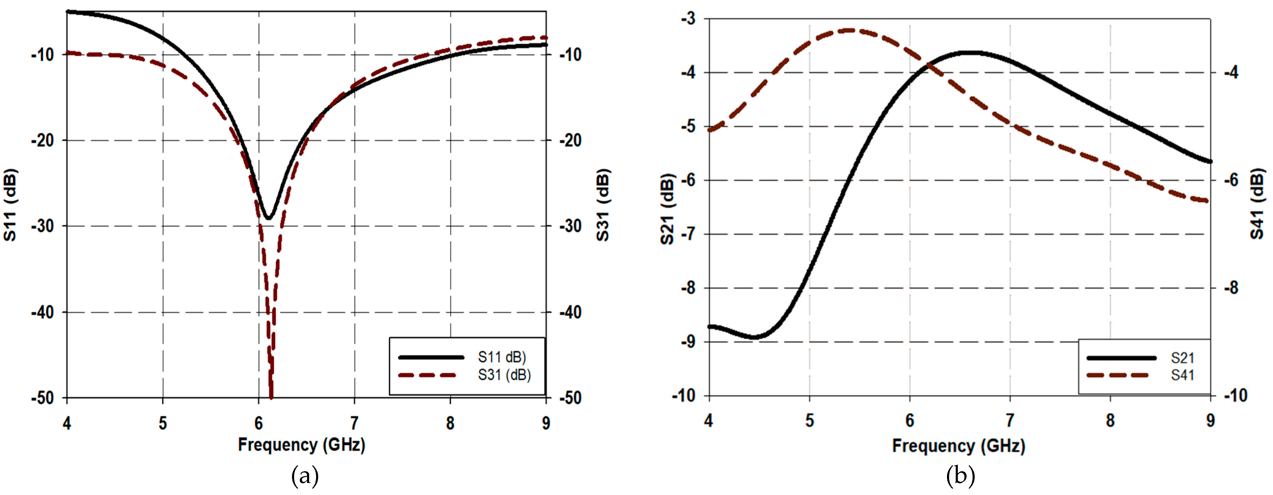
Figure 7 shows the simulated scattering parameters for the conventional branch line coupler, operating at 6GHz. The input reflection coefficient (S
11) and the isolation coefficient between input ports S
31 are presented in
Figure 7a, demonstrating a -30dB excellent match for the conventional BLC at the frequency of interest, 6 GHz, alongside a relative impedance bandwidth of 42.2% (5.214 GHz – 8 GHz), in addition to a perfect isolation of -50 dB. On the other hand,
Figure 7b illustrates the transmission coefficient (S
21) and coupling coefficient (S
41), where it can be shown that the power is divided equally between the output ports (2 and 4) at 6.18 GHz, with a value of -3.8 dB. However, the delivered power declines in both output ports (2, and 4) as the frequency increases, reaching -5.6 dB at the transmission port (port 2) and -6.38 dB at the coupled port (port 4), as shown in
Figure 7b.
3.2. Proposed Quasi-Twisted Branch Line Coupler Structure
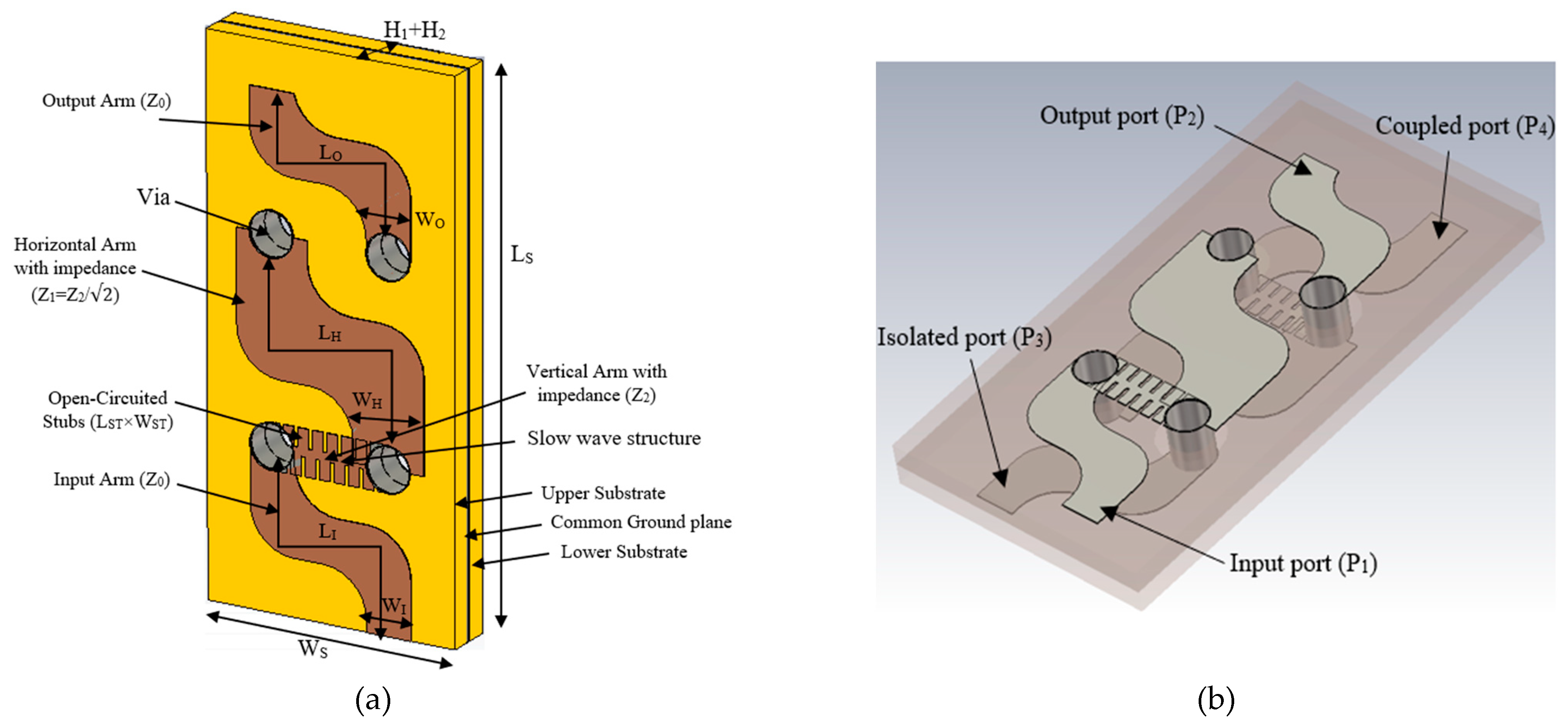
A branch line coupler incorporating a MDL-TL topology has been designed on a double layered 0.8-mm FR-4 substrate, as shown in
Figure 8. The horizontal λ
g/4 dimensions of the conventional branch line coupler of
Figure 1 have been transformed to an MDL-TL-based Z-shape, while the vertical λ
g/4 dimensions have been converted to a periodically loaded open-stub configuration (slow wave structure) to achieve a compactness in the structure.
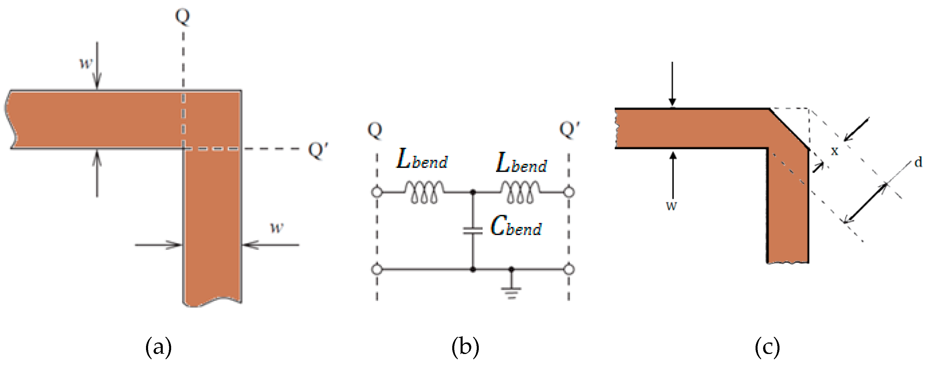
Figure 8a presents a perspective view of the proposed design. The preliminary dimensions of the suggested BLC were selected based on equations (1) and (2) for the conventional MSTL’s width and length, respectively. These dimensions were then slightly optimized using CST. The bending of the meandered Z-shape of the MDL-TL generates a certain reactive component that negatively affects the transmission line performance, such as reflection and transmission coefficients. Therefore, to compensate for this reactance, a 1.5mm radius round-chamfered was implemented at the bending of the MDL-TL. A summary of the designed BLC specifications is presented in
Table 1. The proposed branch line coupler configuration has a quasi-twisted structure as illustrated in the view of
Figure 8b.
The proposed design concept is inspired by twisted cable shapes, aiming to substantially reduce the blank space occupied by traditional BLC circuitry. This was accomplished by dividing the conventional BLC horizontally and interweaving the upper and lower segments in a twisted fashion, utilizing a Z-shaped meandering technique with traditional MSTL components. The design procedure of the suggested BLC of
Figure 8 involves two key steps as follows:
Step1: As shown in
Figure 8, the characteristic impedance of the input, output, coupled, and isolated ports has been selected to be Z
0=50Ω. Also, using equation (1) the relevant lines’ λ
g/4 MSTL (the four input/output ports), shown in
Figure 8, are designed of a width is 1.53mm. On the other hand, the width of the horizontal characteristic’s impedance of Z
1= Z
0/√2, has been calculated as 2.63mm, and further optimized to 2.42mm to realized optimal s-parameters performance. The vertical λ
g/4 length arms with an impedance of Z
2=Z
0 are designed to occupy an optimal small area. The internal and external corners of all the Z-shaped sections are round-chamfered having a radius of 1.5mm to improve the reflection and transmission coefficients as described in
Section 2. The length,
Lo, of the output port (
P2) is less than λ
g/4, which in turn is shorter than the
Lc length of the coupled port (
P4), as shown in
Figure 8b. These modifications in the lengths are necessary to tune the difference between the output ports’ phases to ~90
O. The proposed structure, demonstrated in
Figure 8, provides a novel BLC configuration, which is significantly miniaturized by ~50% as compared to a conventional BLC operating in the same frequency of 6GHz.
Step2: A periodically loaded slow wave structure shown in
Figure 9(any reference to the slow wave structure or figure that you can show explicitly?? – I think this will be
Figure 9) is adopted to design a compact λ
g/4 line with enhanced bandwidth to be accommodated the space limitation introduced due to the folding of the BLC halves and using a double layered Z-shaped meandering technique to realize compactness [
18].
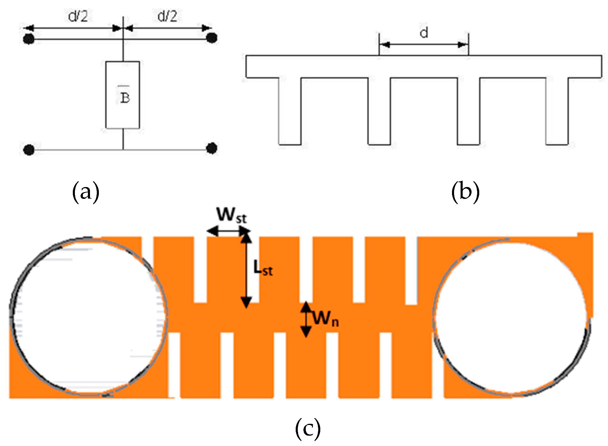
The idea behind a slow wave structure involves the incorporation of shunt capacitors at regular intervals along the length of the transmission line, as illustrated in
Figure 9. This technique results in decreasing both the characteristic impedance and phase velocity, as also can be modelled from equations 7 and 8 below [
18]:
where,
Cp represents the periodically added capacitor at a distance
d along the transmission line.
Z0_loaded and
Z0 denote the characteristic impedance of the loaded and unloaded lines, respectively. On the other hand, reducing the phase velocity facilitates the achievement of an effectively longer electrical length by utilizing a physically shorter length. Additionally, to obtain a line with a specific characteristic impedance, the loading section (
Wn) should possess a higher characteristics impedance, such that its characteristic impedance is decreased to the desired characteristic impedance, usually of 50Ω impedance, after loading.
The relation between the physical length
lp and the electric length
le of the periodically loaded stub TL is given as [
18]:
The added capacitance
Cp, in terms of the known parameters of the loaded and unloaded TL, is given as [
19]:
where
is the angular frequency, and
N is an integer that refers to the stub section’s number.
On the other hand, open stubs with a length of multiples of a quarter wavelength were added in parallel to one pair of branch-line coupler sides, operating as a parallel stub transformer, as reported in [
20]. Therefore, the characteristic impedance of the added stubs attenuates the maxima in return loss characteristics (S11) when the frequency deviates, which, in turn, broadens the bandwidth.
In the proposed configuration, shown in
Figure 8, the slow wave structure is accomplished by inserting alternate slots around the conventional straight MSTL with respective length and width of 2.62 mm and 1.52 mm, which creates rectangular stubs around both sides of the line as shown in
Figure 9c . To create rectangular stubs around the MSTL, slots were placed in an alternate configuration, resulting in stub dimensions of W
st×L
st = 0.234 mm² on both sides of the line as depicted in
Figure 9c. The addition of these slots transforms the 50Ω MSTL to a narrow MSTL with a width of W
n=0.271mm that provides a characteristic impedance of 105.9Ω, which compensates for the shunt impedances of the periodic stubs and results in an overall characteristic impedance that is close to 50Ω.
4. Fabrication and Measurements
The proposed novel miniaturized BLC, shown in
Figure 10, was fabricated on an FR4 substrate with a dielectric constant of 4.4 and a thickness of 0.8 mm, where a thin ground plane, of 70µm thickness, was inserted between the two FR4 substrates, forming a sandwich-like structure. Both substrates were truncated at their corners by a cross-sectional area of 2×5 mm each to expose the ground plane and enable the SMA connector to be easily connected, as illustrated in
Figure 10b.
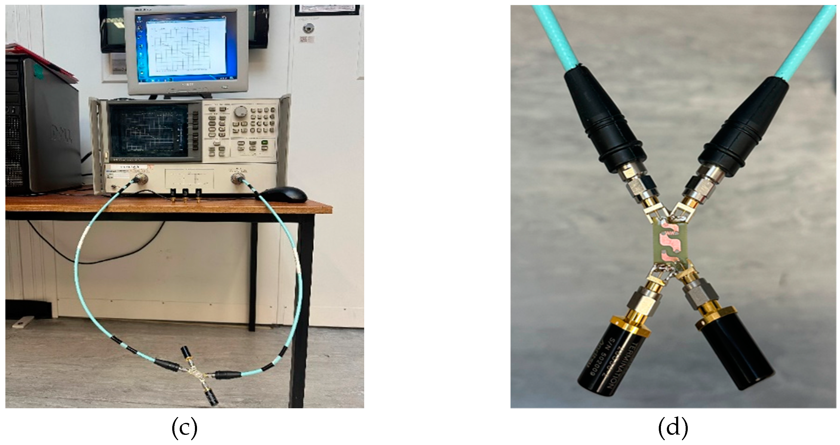
The fabricated novel BLC was measured using an HP 8720B Vector Network Analyzer (VNA), as shown in
Figure 10c. The reflection coefficient, isolation coefficient between input ports 1 and 3, as well as the transmission and coupling coefficients were measured by connecting the relevant ports to the VNA, while the remaining ports were terminated by a 50Ω load to prevent additional mismatch and increase measurements’ reliability, as illustrated in
Figure 10d.
As per the design specifications of the proposed BLC, the required phase difference between the output signals is 90°. This phase difference can be verified by measuring the phases of the transmission coefficients, S
21 and S
43, and coupling coefficients, S
41 and S
23, at the output ports 2 and 4. Once these measurements are carried out, the phase difference can be determined as:
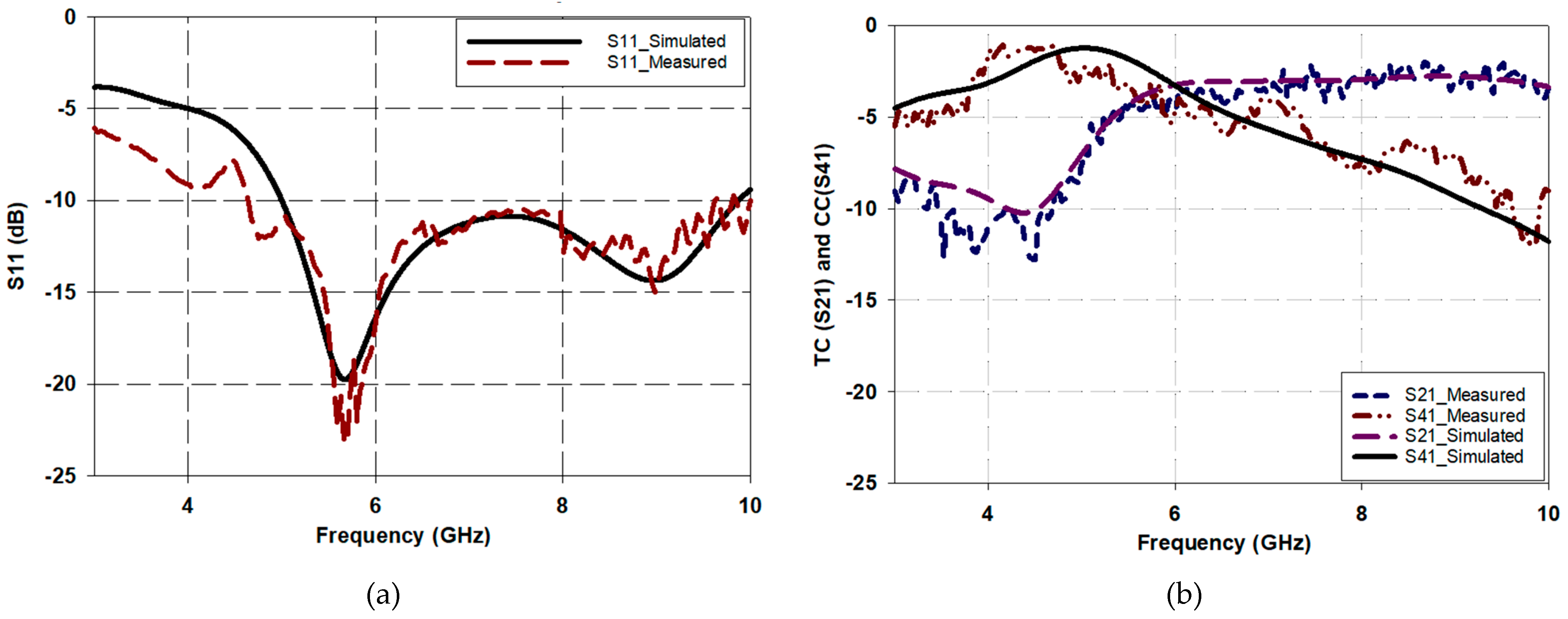
The performance of the proposed BLC is evaluated by observing the 4-port S-parameters magnitudes and phase difference as shown in
Figure 11. The four principal scattering parameters considered in the analysis are: the reflection coefficient (RC) S
11, transmission coefficient (TC) S
21, isolation coefficient (IC) S
31, and coupling coefficient (CC) S
41, when port 1 is excited as the input port. On the other hand, when port 3 is excited, the required scattering parameters S
13, S
23, S
33, and S
43 are considered. Ports 1 and 3 were chosen as they are located on opposite sides of the coupler and are designated as input ports. In addition, from
Figure 11a it is evident that a good agreement is accomplished between the simulated and measured reflection coefficient. For example, the measured -10 dB S
11 bandwidth extends from 4.6 GHz to 10GHz, which corresponds to a relative bandwidth 73.9% compared to a typical bandwidth of ~ 40% from an identical traditional branch line coupler. As a result, the proposed configuration offers a substantial bandwidth enhancement.
The transmission and coupling coefficient, S
21 and S
41, respectively, are presented in
Figure 11b with good agreement between measurements and simulations. From these results, it can be observed that both the transmission and coupling coefficients are -3.9 dB at the desired frequency of 6 GHz, which is close to the ideal value of -3 dB. Notably, S
21 remains higher than -3.5 dB for the entire operating band ranging from 5.8 GHz to 10 GHz. However, the coupling coefficient S
41 gradually degrades with increasing frequency, possibly due to vias and substrate losses since the input port and coupled ports are located on opposite sides of different substrates. Despite this degradation, the power delivered to port 4 remains greater than -7.5 dB up to a frequency of 8 GHz.
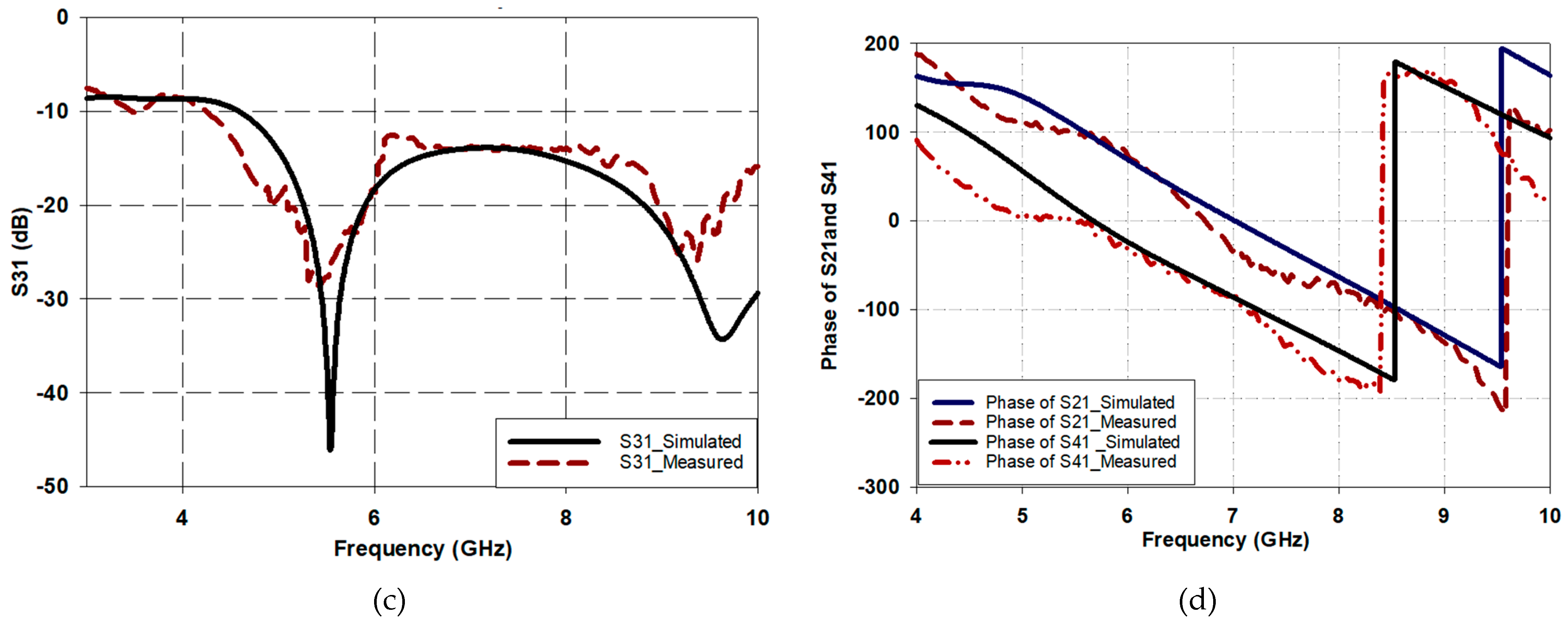
Furthermore, the isolation coefficient between the input ports, S
31, as shown in
Figure 11c demonstrates a magnitude of less than -13 dB throughout the operating band, signifying a good isolation between input ports. This ensures that the proposed BLC meets the necessary design specifications for optimal performance.
Finally,
Figure 11d presents the difference between the phases at the output ports 2 and 4 for input excitations from port 1. As the require a 90° phase difference between the output signals. At the design frequency of 6 GHz, the phase difference between output ports for input from port 1 is (∠S
21-∠S
41=90.50°), which satisfies the required phase difference for typical BLC design specifications. In addition, the phase difference error (PDE) is 0.5° for the deigned frequency of 6 GHz, which is marginal.
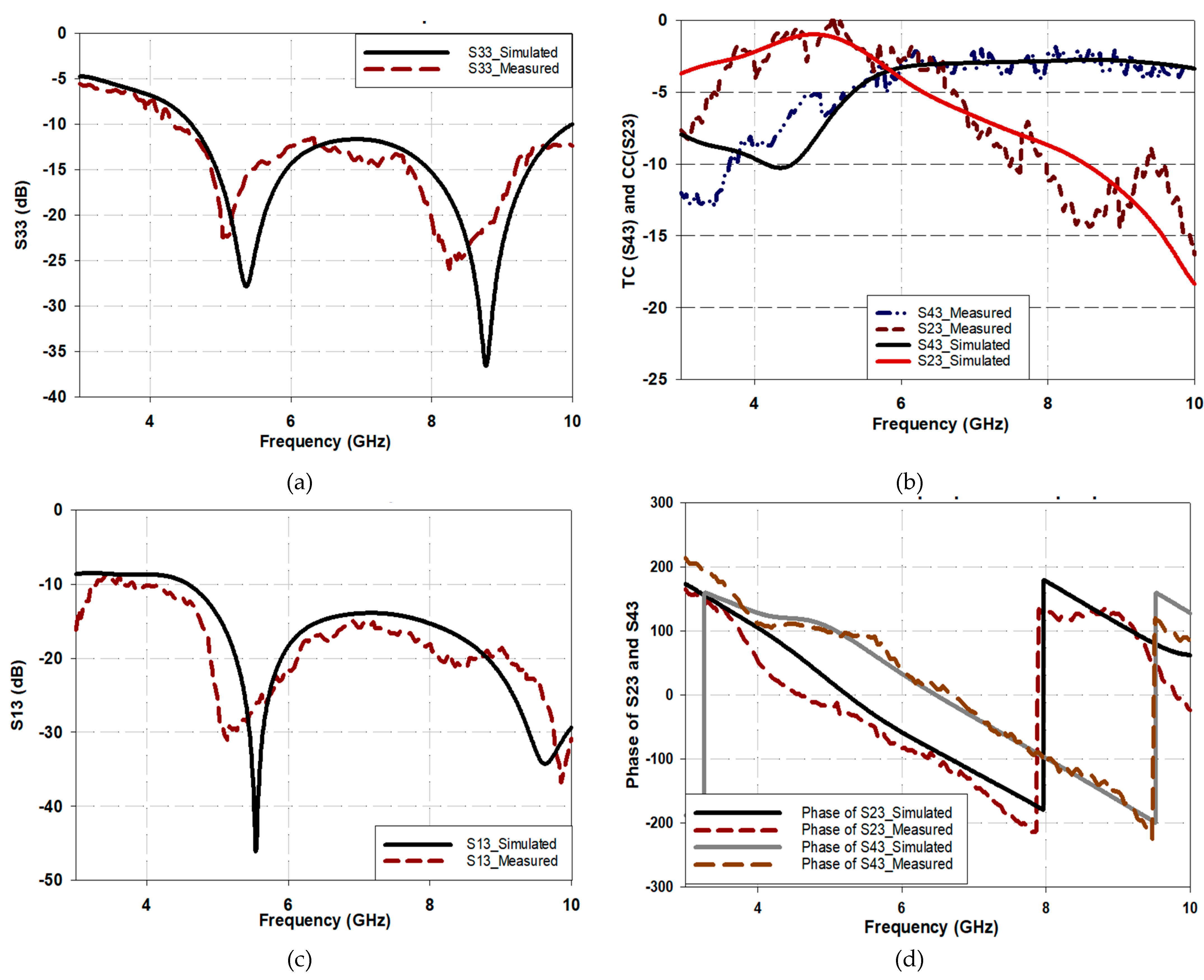
Figure 12 presents the proposed BLC performance when port 3 is excited. From
Figure 12a it is evident that the -10 dB S
33 bandwidth extends from 4.5GHz to 10GHz, which corresponds to a relative bandwidth of 75.8% compared to ~40% for the traditional branch line coupler based on the same design specifications and operating frequency of 6GHz. It should be noted that a marginal difference of 1.9% occurs between the reflection coefficients' bandwidth of S
11 and S
33. The transmission coefficient, S
23, and the coupling coefficient, S
43, for port 3 excitations are illustrated in
Figure 12b. At the target band, i.e at 6 GHz, the transmission, and the coupling coefficients of the proposed BLC design are -3.9 dB, which is close to the ideal value of -3 dB. Notably, the transmission coefficients S
43 remain higher than -3.5 dB for the entire operating band ranging from 5.8 GHz to 10 GHz, and this behavior is consistent throughout this wide operating frequency range. However, the coupling coefficient S
23 gradually degrades with increasing frequency, and this is due to using vias as well as losses inherited from the lossy FR4 substrates, as the input port and coupled ports are located on opposite sides of different substrates. Despite this degradation, the power delivered to port 4 remains greater than -7.5 dB up to a frequency of 8 GHz. In
Figure 12c, the isolation coefficient between input ports, S
13, is depicted. It is evident that S
13 remains less than –14 dB throughout the operating band. It can be concluded that the proposed miniaturized BLC has excellent performance in terms of scattering parameters (S-parameters) compared to a traditional BLC design. Additionally, based on the obtained results, it can also be confirmed that the ports are reciprocal and have the same S-parameters characteristics for all ports. This consolidates the principle that the proposed miniaturized BLC can be used as a unit cell for constructing a Butler matrix, which in turn has the potential use in the development of phased array antenna systems.
Figure 12d illustrates the phase difference between output ports 2 and 4 for input excitations from port 3. At the frequency of 6 GHz, the phase difference between output ports for input from port 3 (∠S
43-∠S
23=94.8°) which meets the requirements of a BLC coupler for good performance. However, a slight discrepancy between the simulated and measured phases is observed for input port 3. This difference may be attributed to fabrication tolerance and the lump solder for SMA feeders. Nevertheless, the phase difference error (PDE) at the design frequency of 6 GHz is 4.8° for the input port 3 excitation.
Table 2 provides a comparison between the performance of the proposed BLC and those of previously published BLC designs. Most of the designs presented in
Table 2 were focused on either improving the bandwidth or reducing the size of the BLC. The proposed work, however, achieves both bandwidth enhancement and size reduction, which is crucial for the design of a 5G system. Furthermore, comparing with respect to the literature, the proposed miniaturized wide band BLC offer other advantages such as; design simplicity, easy to fabricate, smaller phase difference error, and equal power distribution among output port at design frequency 6GHz.
Figure 1.
Geometry of a branch-line coupler.
Figure 1.
Geometry of a branch-line coupler.
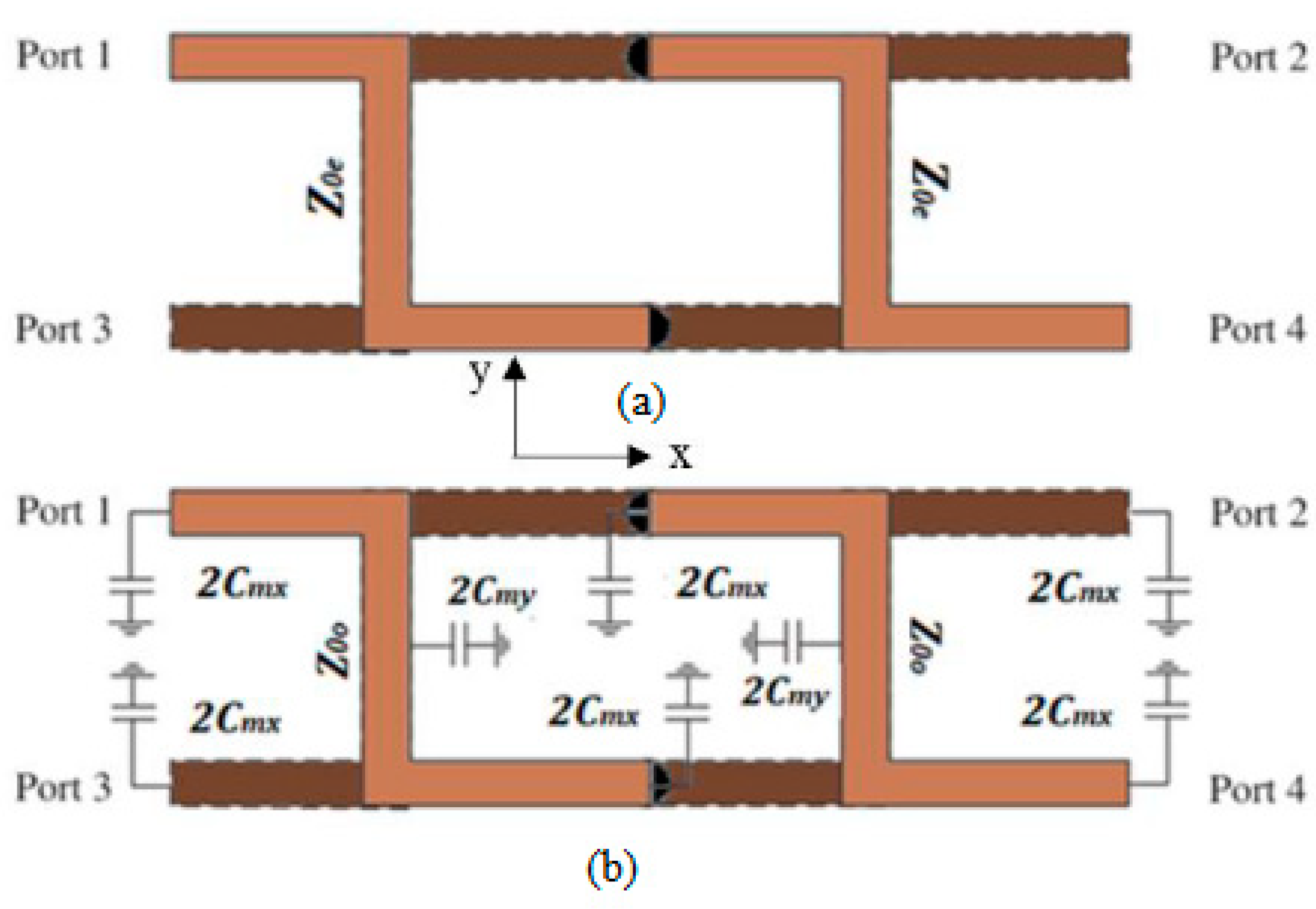
Figure 3.
Double layered MSTL equivalent model (a) Even mode. (b) Odd mode.
Figure 3.
Double layered MSTL equivalent model (a) Even mode. (b) Odd mode.
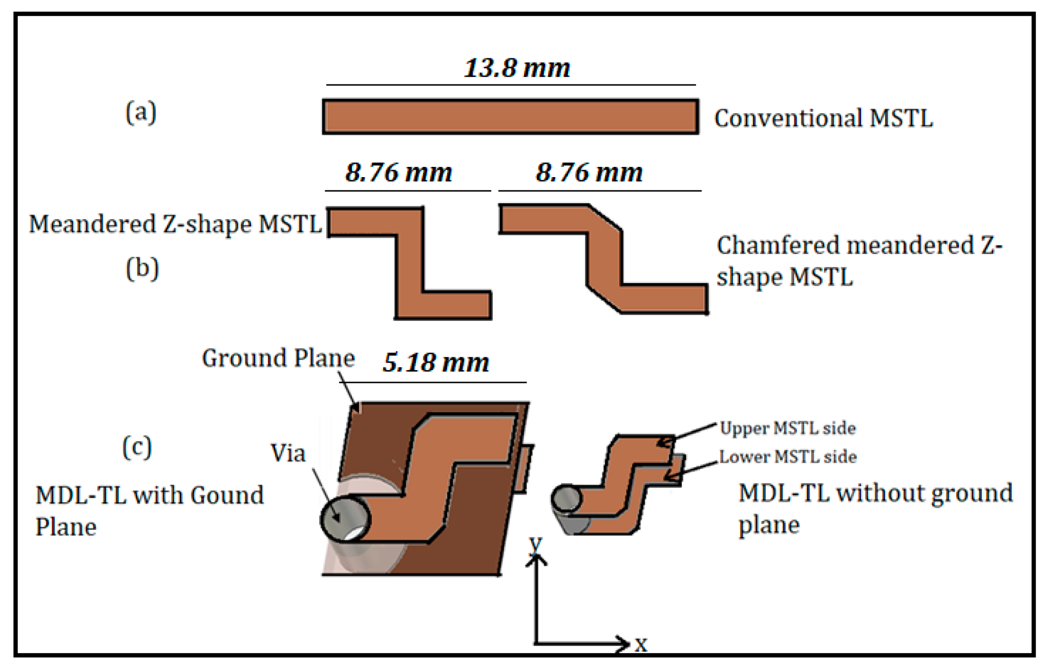
Figure 4.
Various MSTL configurations; (a) Single layer straight MSTL, (b) Single layer meandered MSTL, (c) Double layer meandered MSTL.
Figure 4.
Various MSTL configurations; (a) Single layer straight MSTL, (b) Single layer meandered MSTL, (c) Double layer meandered MSTL.
Figure 5.
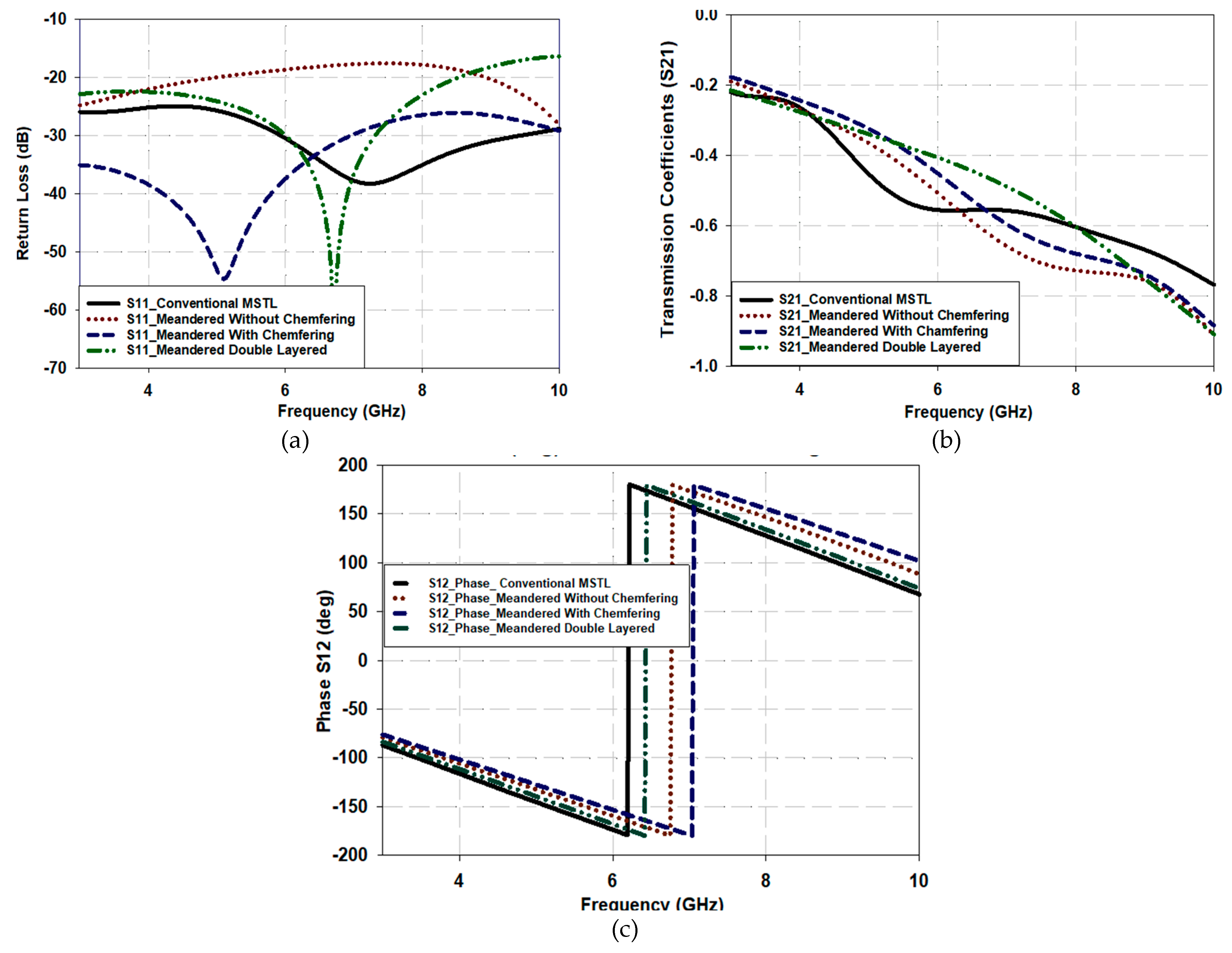
Performance of different MSTL configurations; (a) │S11│, (b) │S21│, (c) Phase of S21 (Output phase).
Figure 5.
Performance of different MSTL configurations; (a) │S11│, (b) │S21│, (c) Phase of S21 (Output phase).
Figure 6.
Structure of the conventional branch coupler operating at 6 GHz.
Figure 6.
Structure of the conventional branch coupler operating at 6 GHz.
Figure 7.
Scattering parameters of conventional BLC; (a) reflection coefficient (S11) and isolation coefficient (S31), (b) Transmission coefficient (S21) and coupling coefficient (S41).
Figure 7.
Scattering parameters of conventional BLC; (a) reflection coefficient (S11) and isolation coefficient (S31), (b) Transmission coefficient (S21) and coupling coefficient (S41).
Figure 8.
Proposed quasi-twisted branch line coupler; (a) Perspective view, (b) frame mode view.
Figure 8.
Proposed quasi-twisted branch line coupler; (a) Perspective view, (b) frame mode view.
Figure 9.
(a) A single periodic section circuit diagram of periodically loaded transmission line, (b) Schematic diagram of periodically loaded line with open stub used as loaded capacitance, and (c) The proposed slow wave structure.
Figure 9.
(a) A single periodic section circuit diagram of periodically loaded transmission line, (b) Schematic diagram of periodically loaded line with open stub used as loaded capacitance, and (c) The proposed slow wave structure.
Figure 10.
(a) BLC prototype, (b) BLC prototype with SMA connectors, (c) Measurement setup system, and (d) Termination of un-fed ports.
Figure 10.
(a) BLC prototype, (b) BLC prototype with SMA connectors, (c) Measurement setup system, and (d) Termination of un-fed ports.
Figure 11.
4-Port S-parameters for the proposed BLC when port 1 is excited, (a) S11, (b) S21, (c) S31, (d) phase difference of the output power.
Figure 11.
4-Port S-parameters for the proposed BLC when port 1 is excited, (a) S11, (b) S21, (c) S31, (d) phase difference of the output power.
Figure 12.
Performance of the proposed BLC when port 3 is excited, (a) S33, (b) S43, (c) S13, (d) phase difference of the output power.
Figure 12.
Performance of the proposed BLC when port 3 is excited, (a) S33, (b) S43, (c) S13, (d) phase difference of the output power.
Table 1.
The design specifications of the suggested BLC.
Table 1.
The design specifications of the suggested BLC.
| Description |
Notation |
Dimension (mm) |
Description |
Notation |
Dimension (mm) |
| Lengths of input arm (P1) and Isolated arm (P3) |
LI |
9.27 |
Coupled arm (P4) length |
Lc |
10.02 |
| All ports' width |
WI |
1.53 |
Via radius |
VR |
0.765 |
| Horizontal arm (port) length |
LH |
8.69 |
Substrates’ thickness |
H1&H2
|
0.8 |
| Horizontal arm (port) Width |
WH |
2.42 |
Substrates’ Length |
LS |
18 |
| Output arm (P2) length |
Lo |
8.52 |
Substrates’ Width |
WS |
8.5 |
| Horizontal arm (port) Width |
WH |
2.42 |
Open-circuited stub length |
LST |
0.625 |
| |
|
|
|
|
|
| Open-circuited stub width |
WST |
0.375 |
Actual circuit area |
Lc×Wc
|
18×6.42 |
Table 2.
Comparison of proposed BLC performance with respect to published designs available in the literature.
Table 2.
Comparison of proposed BLC performance with respect to published designs available in the literature.
| Ref. |
Operating Frequency (GHz) |
Relative Bandwidth (%) |
) |
S11 @ 6GHz (dB) |
S21 @ 6GHz (dB) |
S41 @ 6GHz (dB) |
S31 @ 6GHz (dB) |
PDE error (Deg) |
| [4] |
3.5 |
30.22 |
0.27 ×0.16 |
-27.47 |
-4.4 |
-3.1 |
-26.2 |
3.54 |
| [5] |
2.36 |
31.77 |
0.25 ×0.29 |
-25.5 |
-2.9 |
-3.2 |
-27.5 |
1 |
| [7] |
1.77 |
7.2 |
0.62 ×0.62 |
-35.9 |
-3.1 |
-3 |
-37.9 |
- |
| [8] |
0.9 |
67.7 |
0.2 ×0.2 |
-19.89 |
-3.69 |
-3.67 |
-17.5 |
- |
| [9] |
3 |
50.4 |
0.45×0.25 |
-21 |
-0.95 |
-10.5 |
-29 |
±10 |
| [1] |
3.5 |
40.2 |
0.55×0.65 |
-12 |
-3.19 |
-2.8 |
-15.2 |
-2 |
| [11] |
0.95 |
22.2 |
0.17×0.08 |
-30 |
2.3 |
-3.2 |
29 |
- |
| [12] |
2.4 |
33.3 |
0.2×0.35 |
-20 |
12.5 |
-2.5 |
-20 |
±13 |
| [13] |
2 |
13 (S11<-20) |
0.3×0.3 |
-30 |
-3.5 |
-3.5 |
-27 |
±5 |
| This Work |
6 |
75.8 |
0.3×0.74 |
-14 |
-3.17 |
-3.17 |
-18.9 |
0.5 |
