1. Introduction
Pancreatic and biliary cancers have some of the lowest cure rates, with five-year survival rates of only 12% and 28%, respectively [
1]. Detecting these cancers early is crucial since a more than 50% cure rate can be achieved. However, once these cancers metastasize, they are difficult to treat. The current diagnostic methods include ultrasound, CT, MR cholangiopancreatography, and endoscopic retrograde cholangiopancreatography [
2]. Unfortunately, detecting early cancers of 1 cm or less with these methods is challenging. Histological confirmation is necessary for diagnosis, and ultrasound endoscopy is one of the available diagnostic methods [
3]. It is used to get images, diagnose and locate lesions, and take biopsies [
4]. However, the large outer diameter of the ultrasound endoscope (more than 10 mm) makes it challenging to perform a biopsy in the narrow bile duct or pancreatic duct.
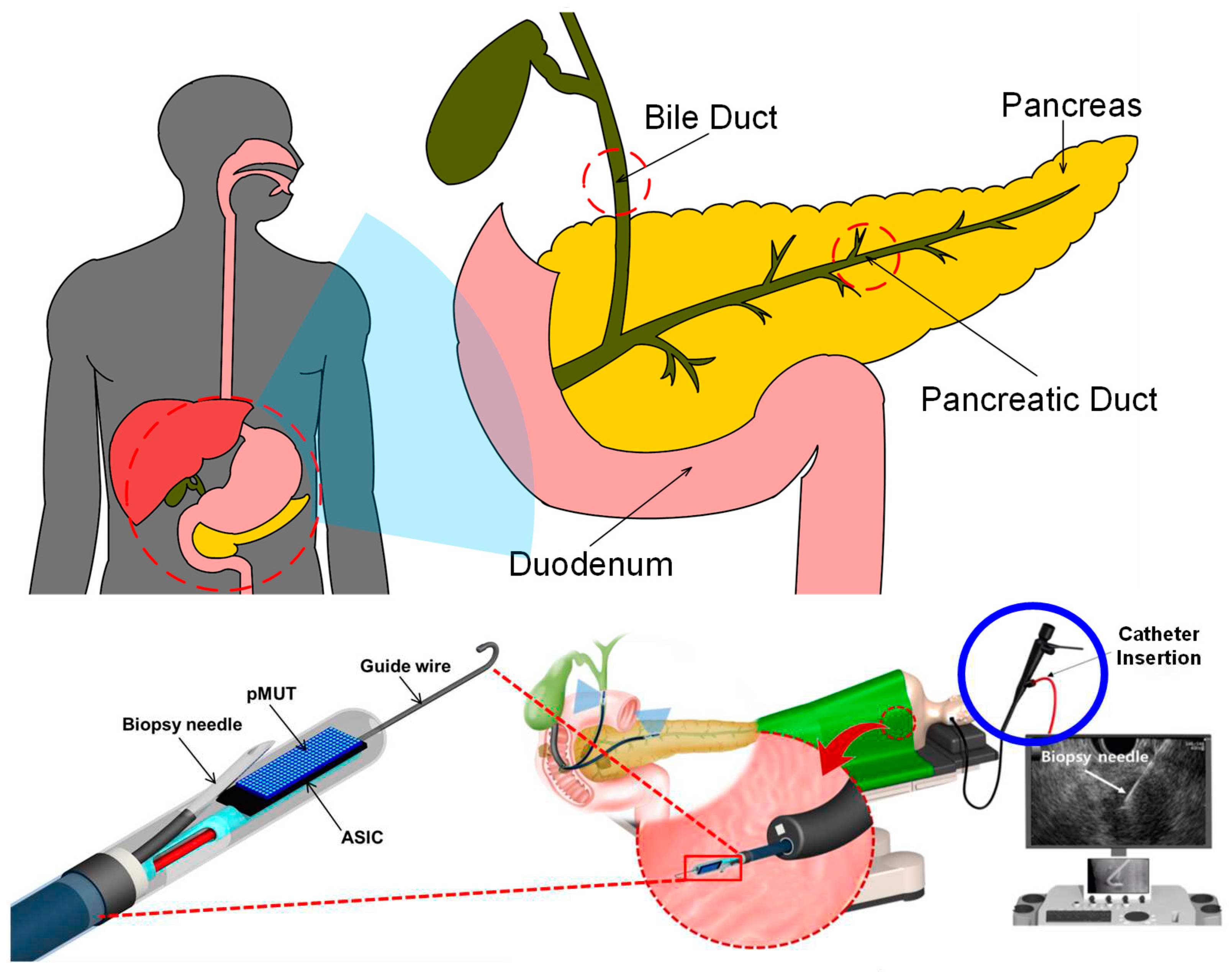
Figure 1 illustrates the need for a catheter to integrate both the transmitter and receiver for ultrasound endoscopy to diagnose pancreaticobiliary disease. This technique carries the risk of heat generation, which can harm living tissue. As a result, the total power consumption must be limited to 0.5W or less. The diameter of the ultrasound endoscope must be smaller than that of the pancreaticobiliary duct, which requires the use of a low-area ASIC. Moreover, the number of input and output wires in the endoscope is severely limited, making it essential to have high detection resolution to guide the needle for tissue biopsy. Therefore, low-power consumption, low-area occupancy implementation with high-resolution imaging is a key requirement for the catheterized application.
First, the transmitter is the main power consumer in an ultrasound system, and it typically uses high-voltage pulses of tens of volts to actuate the transducer. Therefore, reducing the power consumption in the transmitter is crucial. The bipolar-CMOS-DMOS (BCD) or HV process [
5,
6,
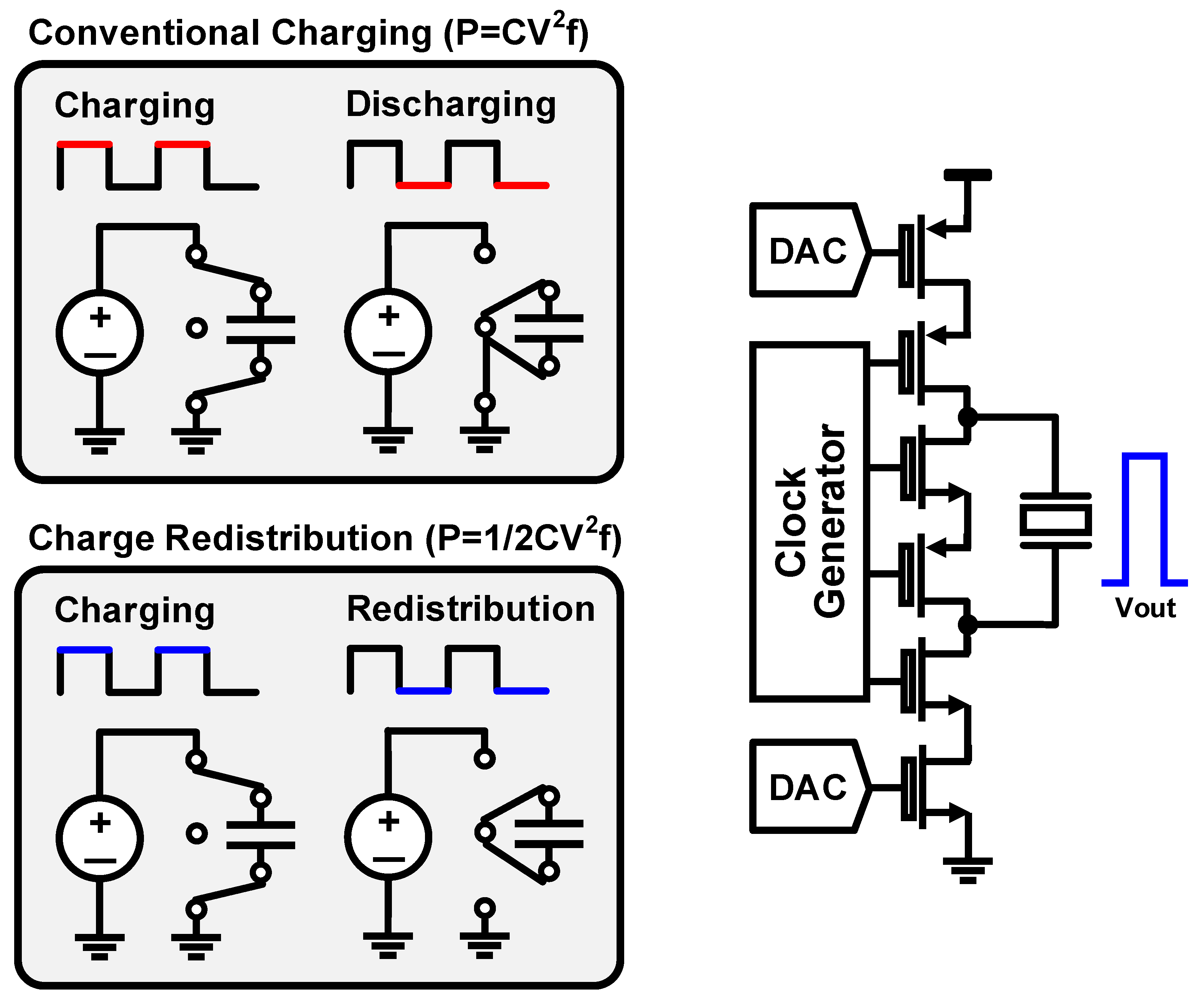
7] is commonly used. Still, it has dynamic power losses that occur due to high voltage switching operation, and it can be expensive to fabricate. An alternative technique to achieve high power efficiency is using the charge redistribution method [
8], which involves stacking PMOS and NMOS alternatively using the standard CMOS process as shown in
Figure 2. However, the 2-level high voltage pulses still generate dynamic power dissipation from the large parasitic capacitance from the transducers.
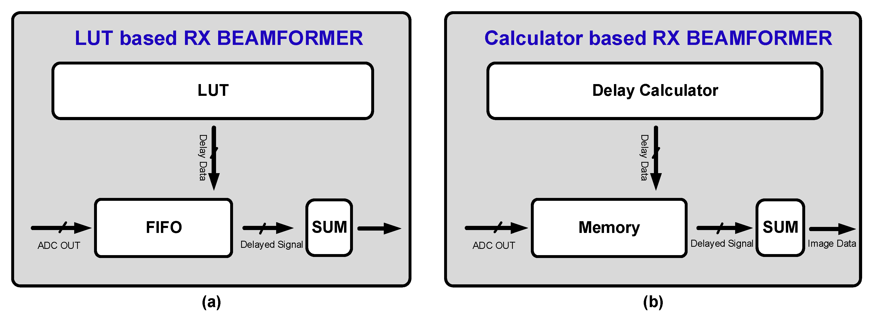
Second, the beamformer is responsible for coordinating the timing of the TX pulse with the timing of the echoes received from the multi-array transducers. To achieve a low-area system, it is crucial to generate delay information efficiently. The delay data can vary depending on the application, but tens of Mb or more data is typically needed to reconstruct a single image. The delay information can be specified in a lookup table (LUT) or internally calculated by the processing unit.
Figure 3 (a) shows the LUT-based architecture [
8,
9,
10,
11,
12,
13], which consists of a LUT that stores the delay data and a FIFO that receives the delay data and performs the beamforming operation. When a signal is received, the delay and stored delay information are processed in the FIFO. The delayed signals are then combined to generate the signal at the corresponding focal point. The more delayed data, the larger the size of the LUT should be, which leads to a significant area overhead. Symmetric delay information was used to minimize the size of the LUTs [
10]. However, it still required a size of over 1 Mb. On the other hand,
Figure 3 (b) shows the delay calculator-based architecture [
14,
15,
16,
17]. The output signals from all the ADCs are stored in a memory. The delay calculator generates the delay information for each focal point. To get the corresponding delayed signal, the address in the memory is accessed by a calculated delay. The calculator is utilized instead of LUTs to save area, and it uses power-consuming computation, which results in a smaller area with more significant power consumption.
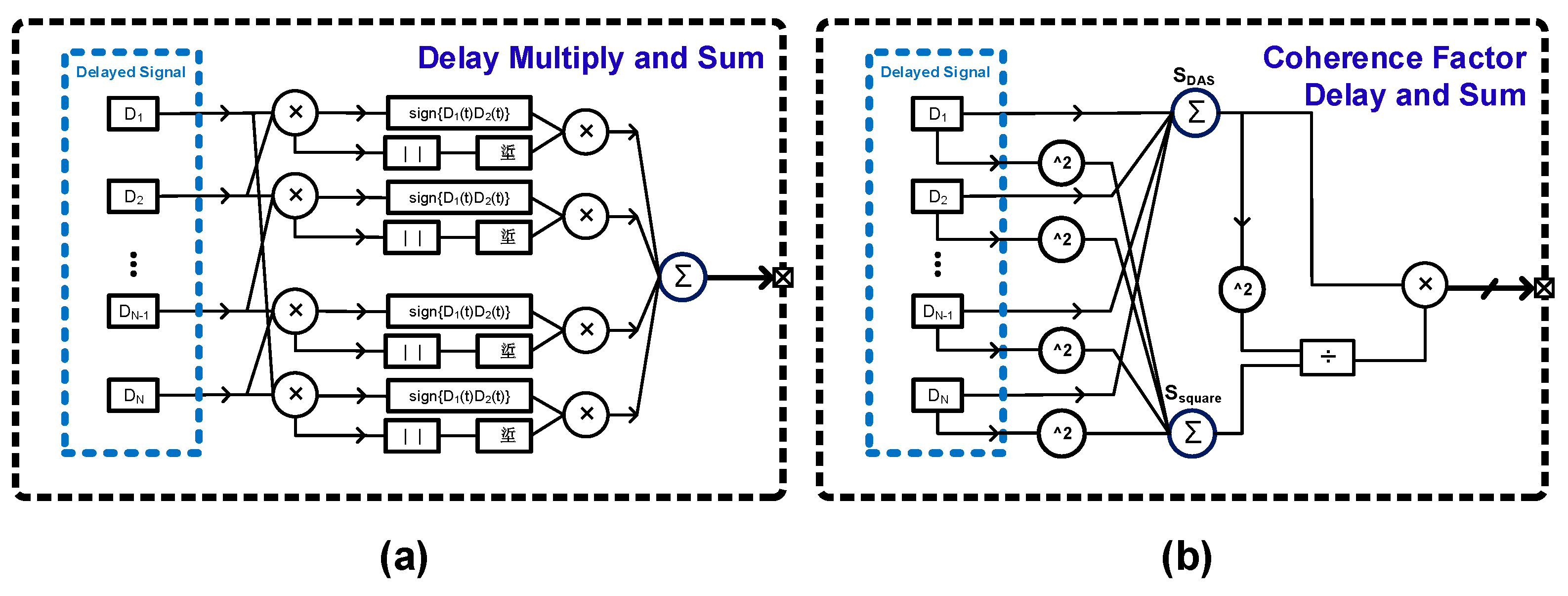
Last but not least, considering the beamforming algorithm to obtain high-quality images using a reasonable number of channels is essential. The conventional delay and sum (DAS) algorithm [
19] has some limitations in improving the lateral resolution and sidelobe rejection ratio, which are essential factors in image quality. Other algorithms have been developed to address these limitations, as shown in
Figure 4. These algorithms are typically implemented through external DSPs due to their high computational requirements. For example, a delayed multiplication and summation algorithm [
20] improves the lateral resolution of an image through additional multiplication and square root operations. Another algorithm introduces a coherence factor [
21] to reduce the number of arithmetic functions compared to [
20]. However, even with these improvements, the algorithms still require division operations, which can be computationally expensive.
With the above considerations, we propose an ultrasound beamforming application specific integrated circuit (ASIC) that is both efficient in terms of power and area. The ASIC includes three key features:
A three-level bi-phasic charge redistribution HV (CRHV) TX pulser that uses a standard CMOS process to increase power efficiency.
A hybrid beamforming architecture with an analog subarray beamformer and calculator-based digital beamformer that uses FIFO instead of memory to achieve a low-area system.
A hardware-efficient Shift Coherence Factor (SCF) beamforming algorithm that produces high-resolution images.
The paper is organized as follows. Chapter 2 introduces the block diagram and system features. Chapter 3 covers the implementation of the TX pulser, analog subarray beamformer, delay generator, and SCF beamformer. Chapter 4 presents the implementation results. Chapter 5 includes a discussion. Chapter 6 concludes the paper.
2. System Features
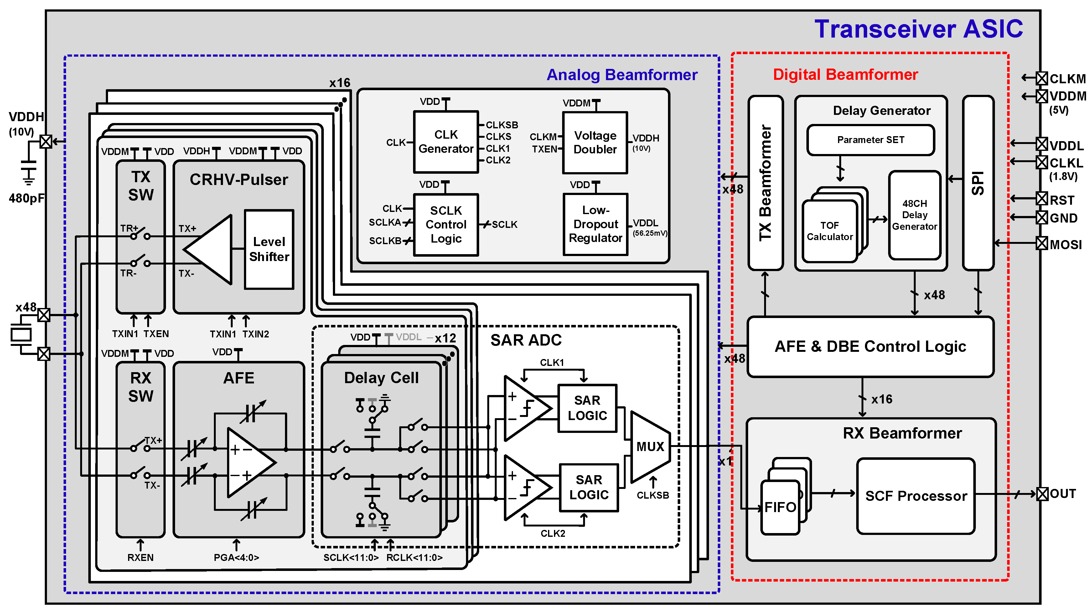
The proposed system is characterized by low power consumption, low area occupancy, and high-resolution image acquisition. To achieve low power consumption, we implemented a TX pulser based on charge redistribution and low area occupancy; a non-memory structure has been implemented using a delay generator and FIFO, and an analog subarray architecture has been used to mitigate the delay resolution and the number of channels in the digital beamformer. Finally, to achieve high-resolution image acquisition, the center frequency is set to 7.5MHz to enable the detection of the biopsy needle with high axial resolution. In addition, the SCF algorithm has been implemented to ensure low sidelobe and high lateral resolution, allowing for accurate biopsy needle guidance.
Figure 5 shows the block diagram of the overall system. The system operates by updating the parameter information of the transducer via the SPI interface. Then, it calculates the delay signal for TX beamforming and determines the time when the signal for each focal point arrives at the sensor through the updated parameters. This information is then used to generate the delay data. The delay data is utilized to perform beamforming of the received echo signal, which is further processed through the SCF algorithm to produce high-resolution image data. As a result, the system requires minimal input and output wires, except for the transducer interface, which only consists of input wires for power, clock, reset, and SPI communication and a multi-bit output wire for image data output.
3. Beamformer Implementation
3.1. CRHV TX Pulser
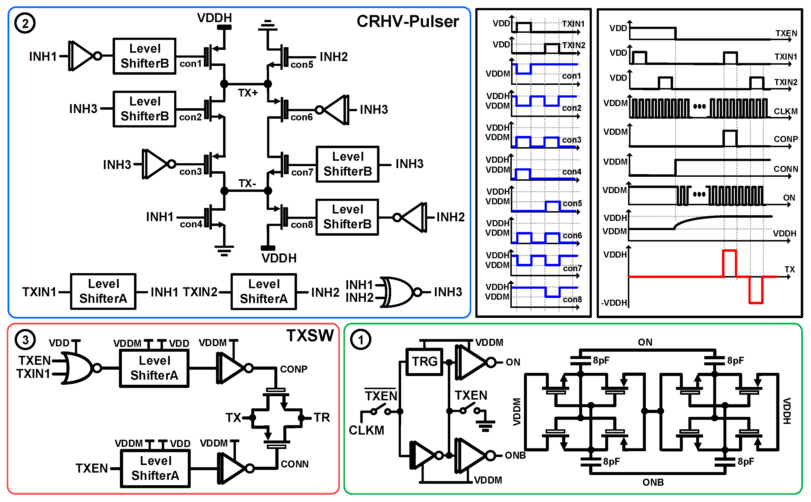
Figure 6 depicts the transmitter block and timing diagram. The transmitter receives a 5V power supply (VDDM) and a 60MHz clock signal (CLKM) from an external source. The signal control logic generates the inputs TXIN1, TXIN2, and TXEN. A voltage doubler generates VDDH, a 10V power source for the high-voltage pulser. To reduce power consumption, CLKM is only asserted when TXEN is 0. The CRHV-pulser takes TXIN1 and TXIN2 as inputs and produces cont1 to cont8 to drive the stacked NMOS and PMOS gates through the level shifters and logic gates. The resulting TX+ and TX- voltage pulse swings from VDDH to -VDDH and is applied to the transducer via the high voltage switch (TXSW). TXSW uses standard CMOS and is implemented using the TXIN1 signal and a level shifter to receive a differential high voltage of 20V.
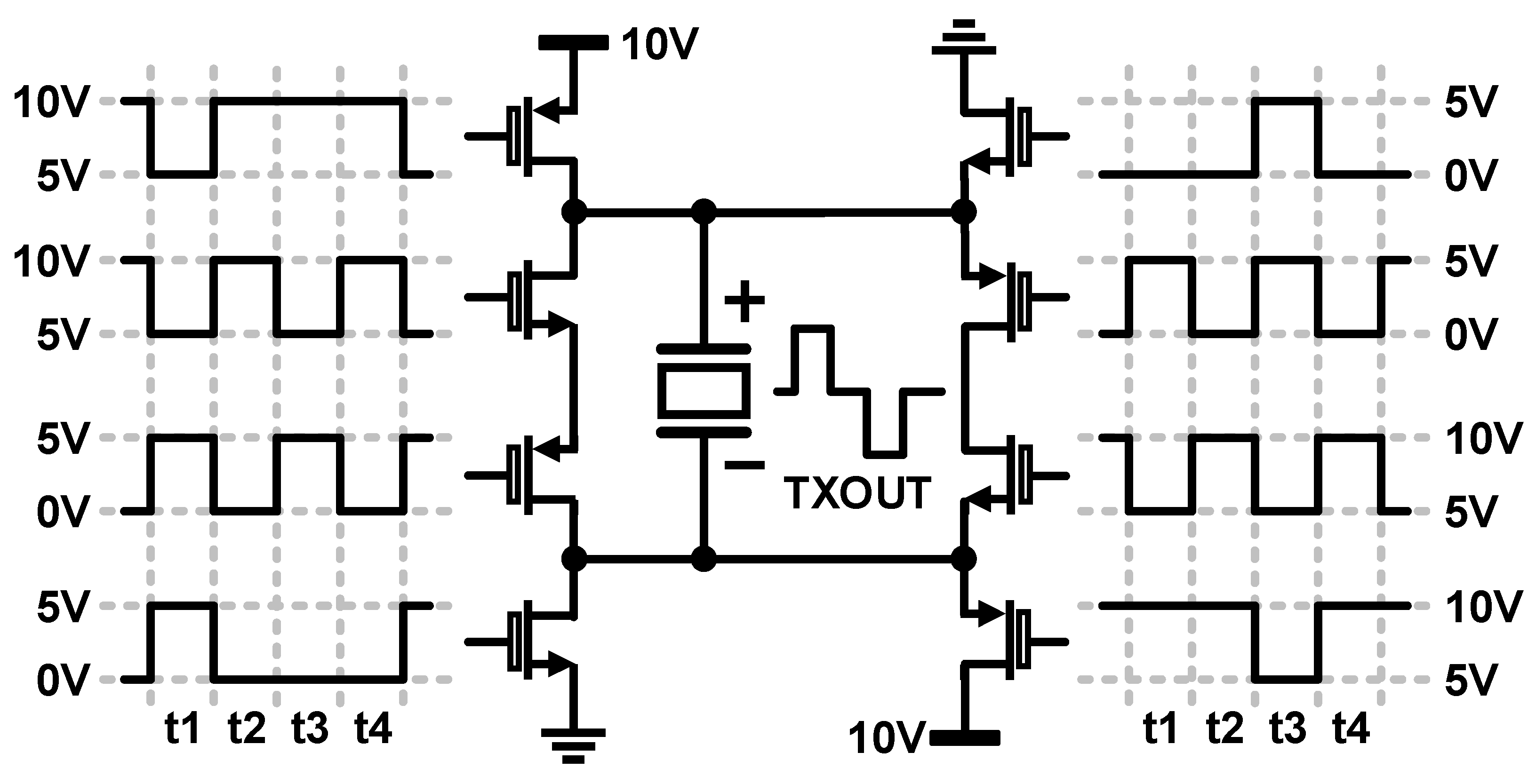
Figure 7 illustrates the detailed operation of the CRHV pulser. The pulser uses a full-bridge configuration to generate pulses differentially with a voltage of 20 Vpp. To utilize the standard CMOS process, the PMOS and NMOS are stacked alternately. During t1, the top left PMOS and the bottom left NMOS turn on, supplying 10V to the positive terminal of the transducer and 0V to the negative terminal. In t2, the floated output is shorted by the NMOS and PMOS in the middle through charge redistribution. Similarly, during t3 and t4, the transducer is charged and charge-redistributed respectively. Therefore, the three-level 20V output pulses effectively drive the transducer, which reduces the dynamic power by 50%, compared to the conventional charge redistribution architecture [
8].
3.2. Delay Generator
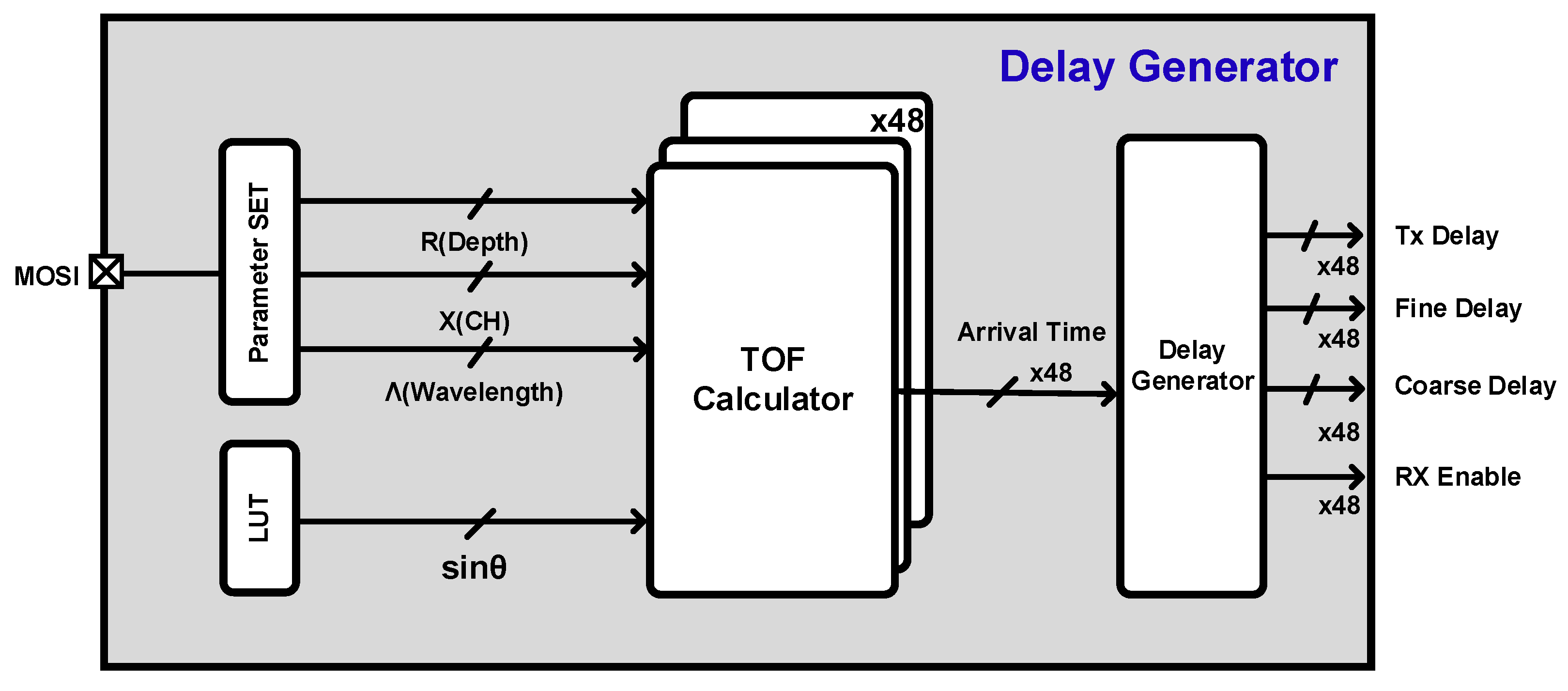
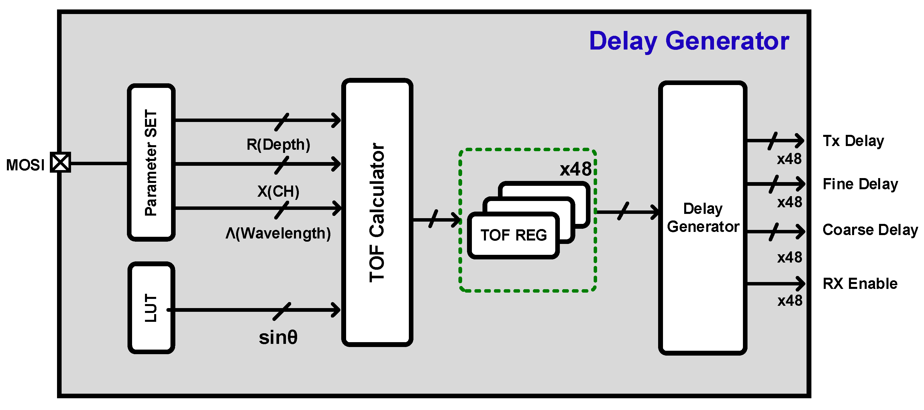
Figure 8 shows the proposed structure of the delay generator. It utilizes SPI communication to update the scan depth (R), number of channels (X), and wavelength. With the updated parameters and the stored sine values in LUT, the time-of-flight (TOF) parameters are calculated. The TOF calculator is a circuit implemented using the Taylor approximation [
18] to reduce computation. Instead of the traditional TOF calculation method that requires finding the distance between each transducer element and the focal point, the proposed structure implements an additional calculation block that uses the TOF to calculate inter-channel delay for the signal at each focus. The delay generator block calculates the delay data from the difference between the minimum TOF data and the TOF data of the other channels. The output signals from this block are TX delay data, fine(analog) delay data, coarse(digital) delay data, and RX switch-on signal. The TX delay is calculated based on a focal point that is half the scan depth per scan line. The fine delay calculates the delay between the three adjacent channels that the analog beamformer will be beamforming. Coarse delay calculates the delay between the 16 channels processed by the analog beamformer and then processed by the digital beamformer. Finally, the RX Enable signal is used to activate the RX switches based on the timing of the first signal to arrive on each channel in the calculated TOF data. By reducing the complexity of the TOF calculations, the proposed delay generator achieves relatively low power consumption and low area occupancy. As a result, the proposed structure offers an efficient way to perform beamforming.
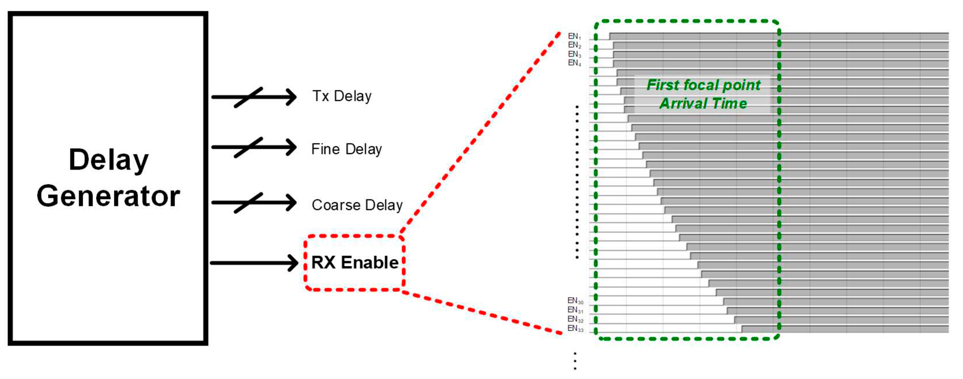
A memoryless structure can be realized using an RX enable signal generated by the delay generator block. As shown in
Figure 9, an RX enable signal is turned on by calculating when the echo signal reaches the focus and returns to each channel based on the TX beamforming signal. When the signal is on, the RX switch is turned on, and the delay signal calculated for each channel is updated simultaneously with the reception of the echo signal on each channel. RX beamforming can be performed without storing all the echo signals in memory because the delay information of the corresponding focal point can be calculated from the TOF data at the same time as the echo signal is received. Therefore, the signals received in real-time can be kept as input signals with their corresponding delay data using a FIFO and then exported to the output.
3.3. Hybrid Subarray Beamforming Architecture
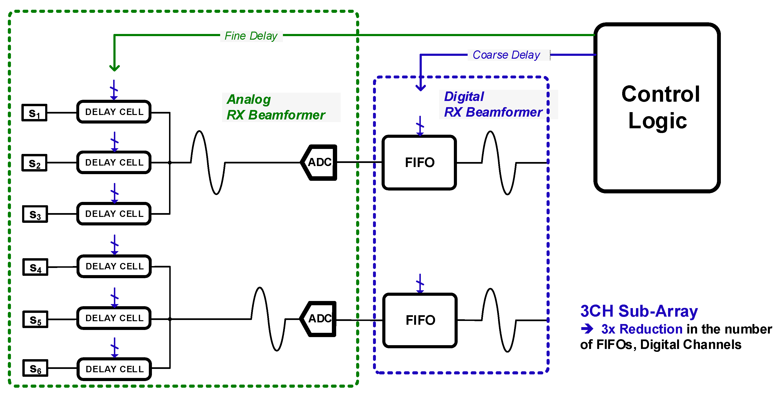
Figure 10 illustrates the use of a hybrid subarray beamforming architecture. This architecture employs both an analog RX beamformer [
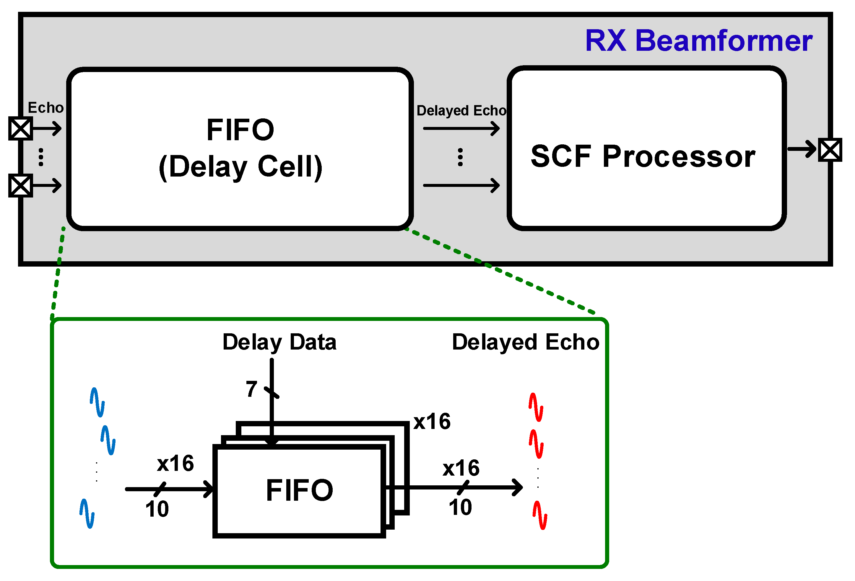
22] and a digital RX beamformer. The analog beamformer is used to focus the signals between adjacent channels with small delays, while the digital beamformer is used to enhance the signal between relatively distant channels with large delays. To reduce the number of delay cells required for the digital beamformer, we use a 3-channel analog subarray, which reduces the number of delay cells required by a factor of three.
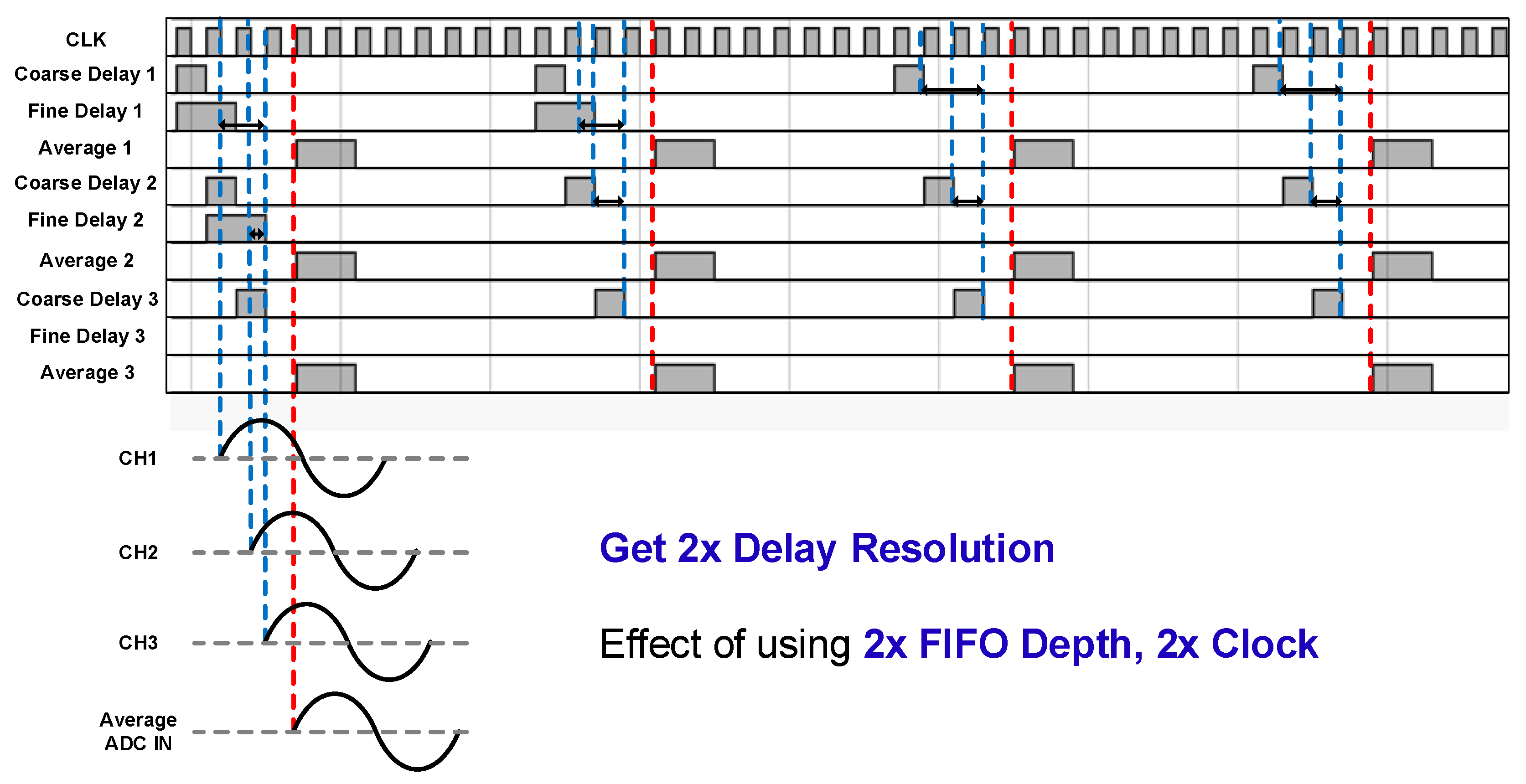
The waveform in
Figure 11 represents a beamforming operation that utilizes fine delay in an analog beamformer. There are three signals controlling the analog beamformer: the coarse delay, fine delay, and average signals. The coarse delay and fine delay signals indicate when the ADC is sampling, while the average signal is provided by adding the outputs of the three channels of the delay cells in the analog beamformer to perform a summation operation. To achieve a delay resolution 16 times higher, while using a clock 8 times the center frequency, the coarse delay signal is sampled through the positive edge, and the fine delay signal is sampled through the negative edge. This provides the same effect as using 1/3 FIFOs in a digital beamformer while using twice the clock and twice the FIFO depth.
3.4. Digital RX Beamformer
A digital RX beamformer structure is illustrated in
Figure 12. The beamformer consists of two main components: a delay cell (FIFO) and an SCF processing block. The FIFO is designed to manage the delays that occur when the delay is generated using the scan depth of the target system and the transducer's parameters. The signal that has been delayed and phase-matched through the FIFO is then directed to the input of the SCF processing block for the proposed beamforming algorithm to enhance the imaging quality.
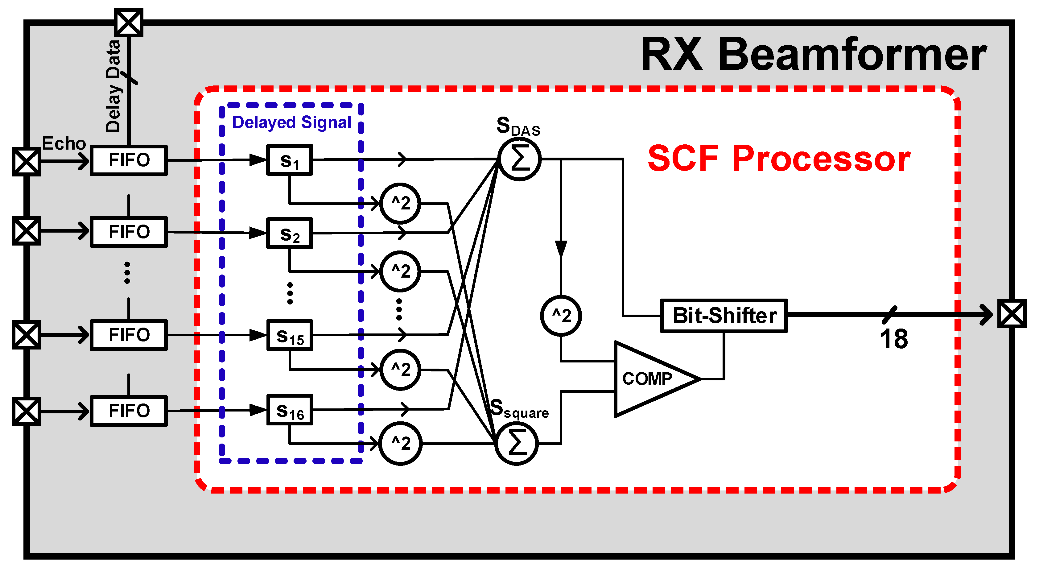
Figure 13 shows the structure of the SCF processor. Compared to the structure that utilizes the coherence factor [
23], the division calculation is implemented with the help of a comparator. The output of the comparator is determined based on the difference between the two input values. There is also a bit shifter that multiplies the output of delay and sum by a coherence factor. The comparator compares the two values and produces an output rounded to a power of two based on the magnitude of the difference. Bit shifting is used to implement the comparator as it only requires comparing the difference in magnitude while multiplying by a power of two, which is not computationally intensive. The output of the comparator is then applied to the bit shifter, which shifts the bits left or right. Applying the coherence factor through the hardware efficient implementation results in improved lateral resolution and sidelobes. This is because the correlation coefficient increases the signal-to-noise ratio from the focal point, with negligible errors from the rounded output from the bit shifter.
4. Implementation Results
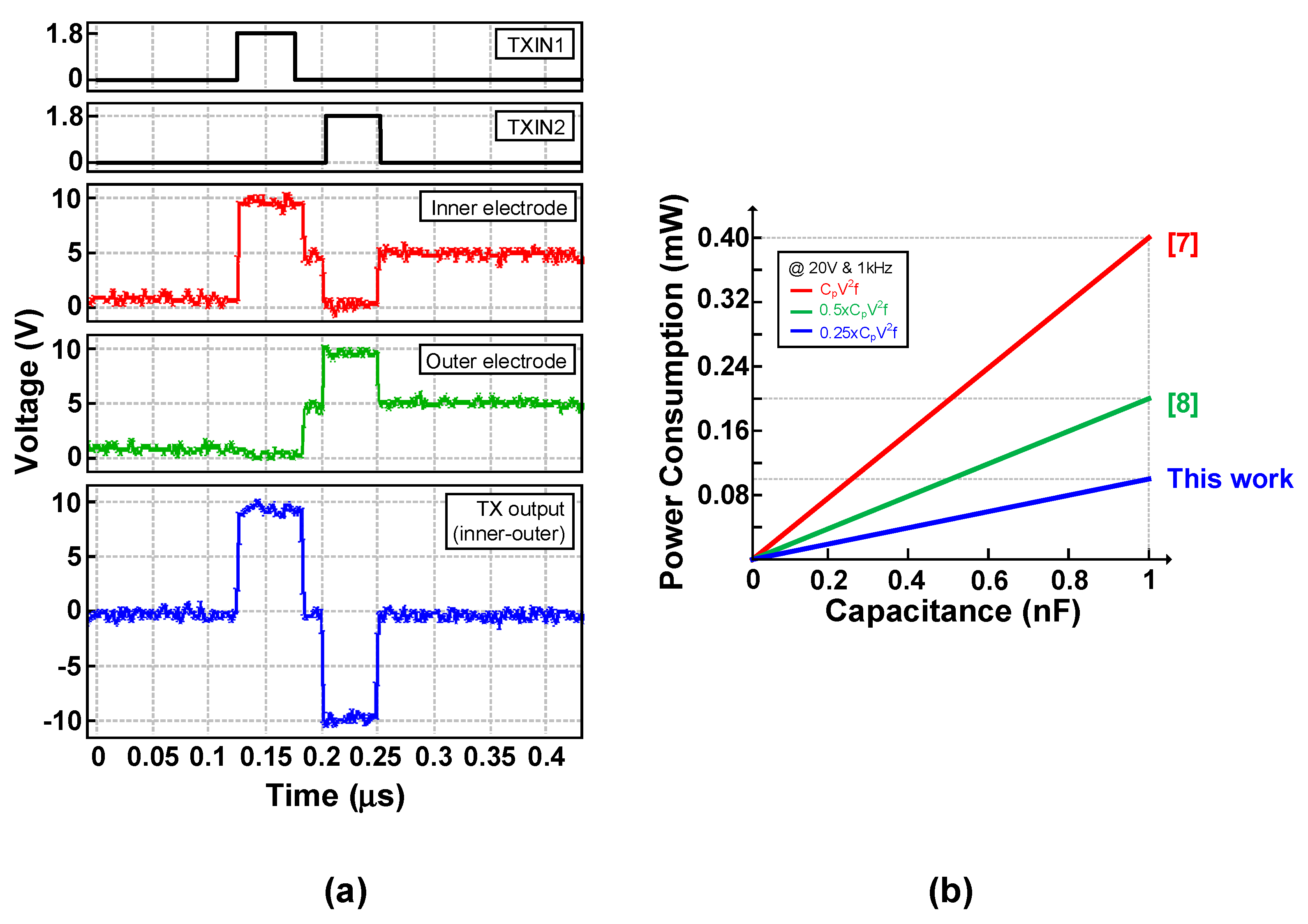
Figure 14(a) shows the waveform measurement for the CRHV pulser. This component receives TXIN1 and TXIN2 signals from the signal control block and generates an output pulse that swings differentially by 20 Vpp and operates at 7.5 MHz, enabling the functionality of the pulser. On the other hand,
Figure 14(b) shows the dynamic power loss of the capacitance in comparison to other references. The proposed work has demonstrated significantly lower dynamic power loss when compared to [
7,
8].
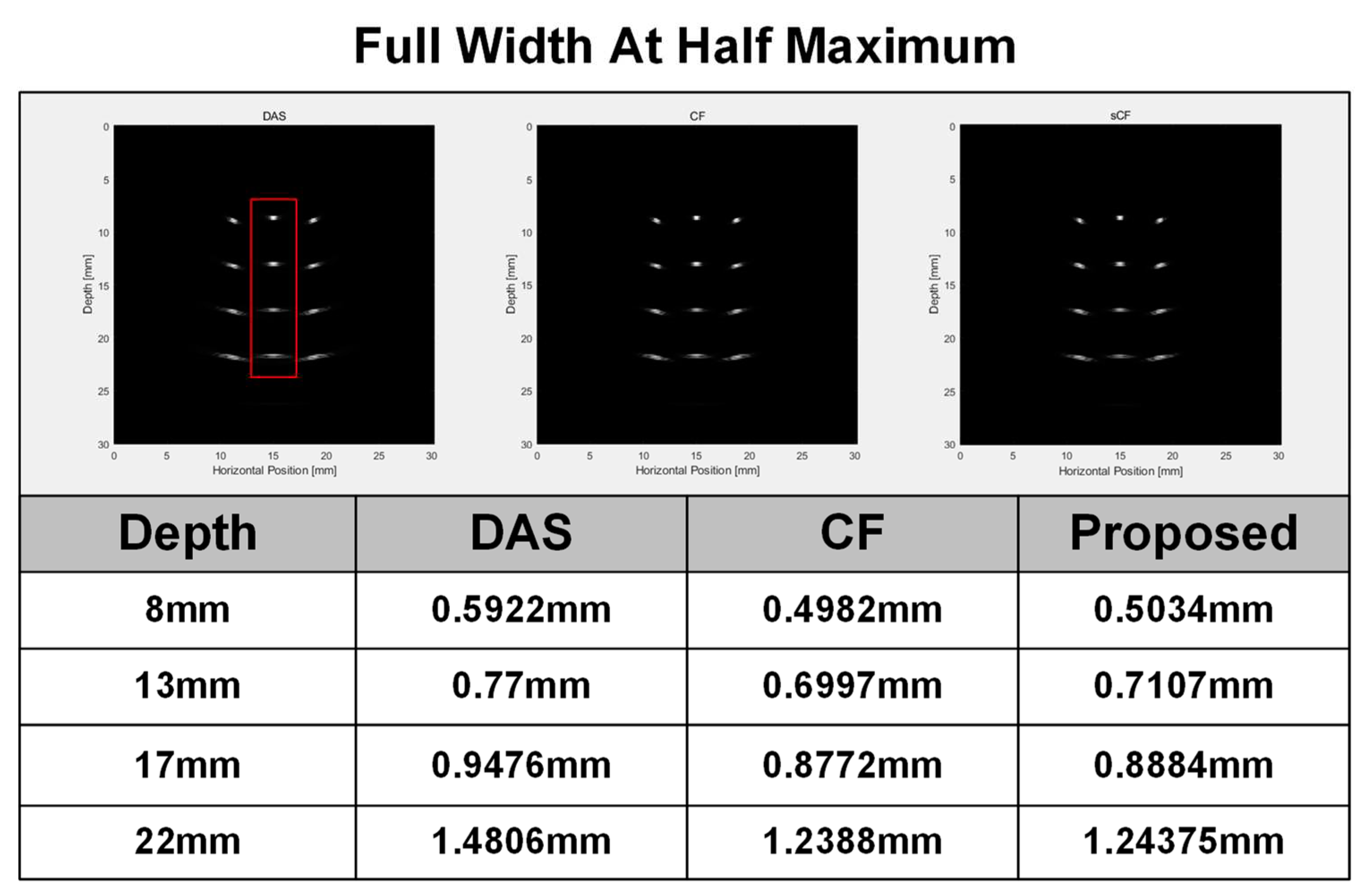
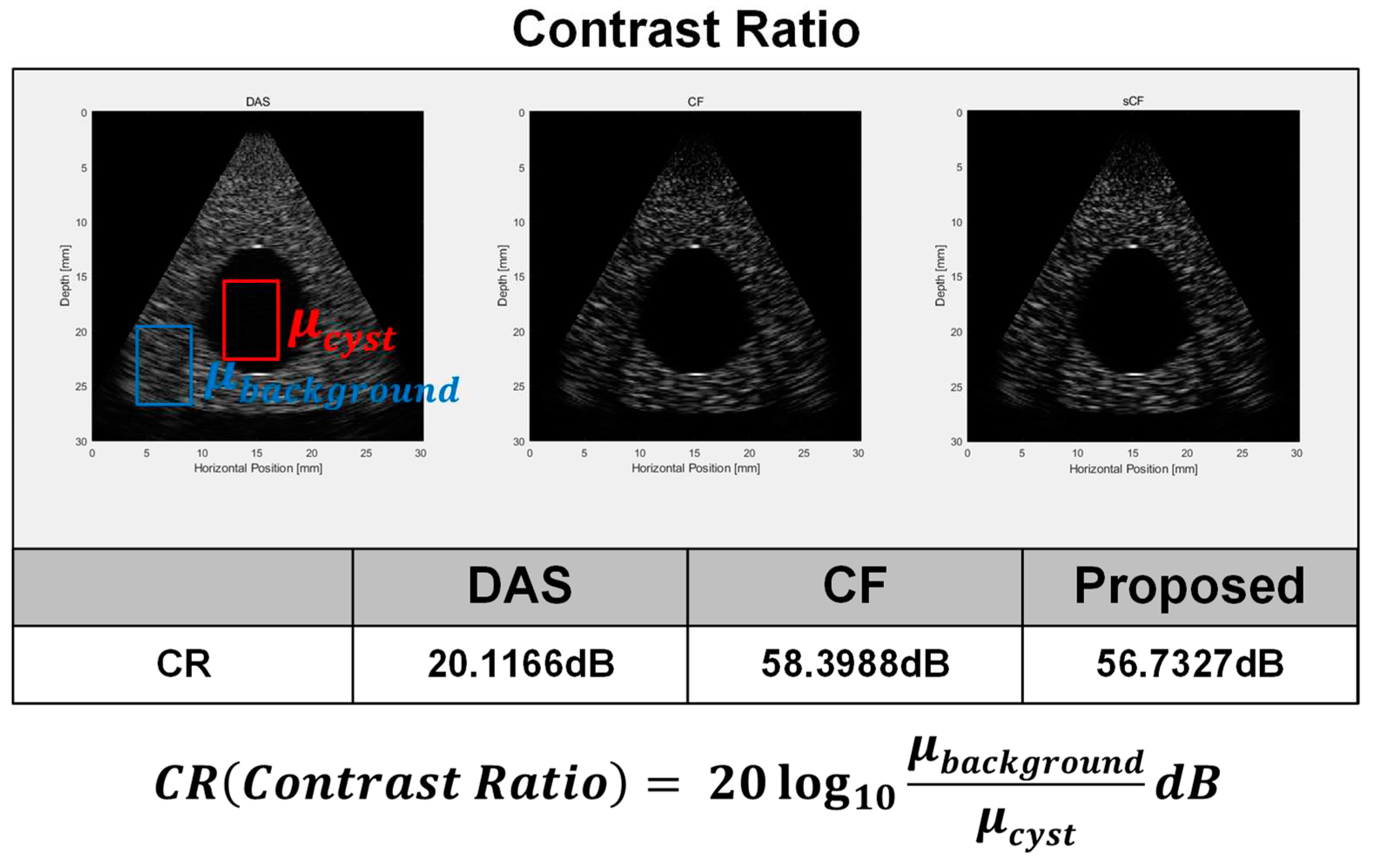
The proposed algorithm, Shift Coherence Factor (SCF), was compared to DAS and CF algorithms based on their lateral resolution performance, as shown in
Figure 15. Since the axial resolution is determined by the frequency of the transducer, the lateral resolution was used to compare the three algorithms. The lateral resolution was tested at depths of 8mm, 13mm, 17mm, and 22mm. Results showed that the SCF algorithm outperformed the DAS algorithm by about 20% at all depths. The SCF algorithm also showed a similar level of resolution compared to the CF algorithm.
Figure 16 presents a comparison of contrast ratios (CR) while viewing the sidelobe. The CR was calculated by contrasting the average brightness of the cyst and the highly reflective background. A lower CR indicates that the sidelobe is more extensive, while a higher CR implies smaller sidelobes. The results reveal that the proposed SCF algorithm enhances performance by approximately 36 dB over DAS. Therefore, we can conclude that the hardware-efficient SCF algorithm does not suffer from significant performance degradation as compared to the computationally intensive CF algorithm.
Table 1 showcases the simulated utilization levels of FPGA synthesis using VIVADO for various beamforming algorithms, with a focus on the RX beamformer. Specifically, the comparison is made between the DAS algorithm, the CF algorithm, and the proposed SCF algorithm. The table compares FPGA utilization of logic, memory, register, RAM, and DSP. The results indicate that the SCF algorithm only differs from DAS by approximately 3% in Logic LUTs and shows no significant difference in overall utilization. On the other hand, the CF algorithm implemented with high precision uses more than 50% of logic LUTs and over 30% of DSPs. In other words, the proposed SCF algorithm does not significantly increase the amount of computation compared to DAS.
Table 2 compares the power consumption of different algorithms after FPGA synthesis. Among them, DAS consumes the least power due to its simplicity. The proposed algorithm consumes approximately 5% more power than DAS. Additionally, the CF implemented using single precision consumes around 30% more power than the proposed SCF. The additional power consumption of SCF is relatively small compared to the CF because it reduces the amount of computation.
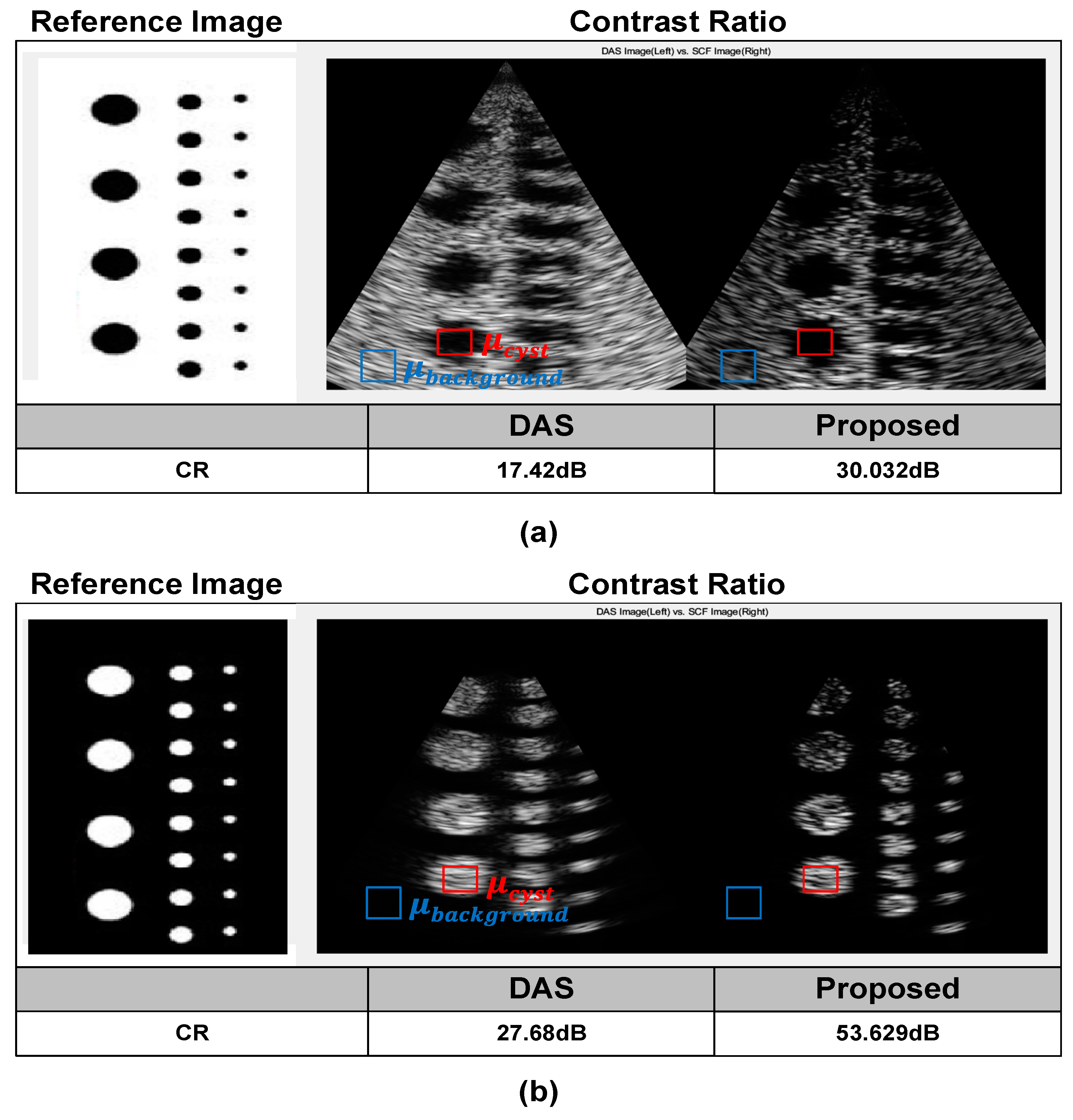
Figure 17 demonstrates the results of using ASIC to reconstruct the image by producing the echo signal as a matrix based on the reference image. On comparing the pixel values of the image data directly, the CR of the background and cyst parts are calculated. The results of DAS and CF shown in
Figure 17 (a) are 17.42 dB and 30.032 dB, respectively, exhibiting a difference of about 13 dB. By examining the images from one focal point each, we can detect where the image is smeared due to sidelobes. The proposed SCF makes the boundary between the cyst and background sharp, as shown in
Figure 17(b), which results from inverting the image from
Figure 17(a). It is observed that the image is relatively sharper, with values of 27.68 dB and 53.629 dB, respectively. The effect of sidelobes appearing in unwanted areas is more prominent in DAS.
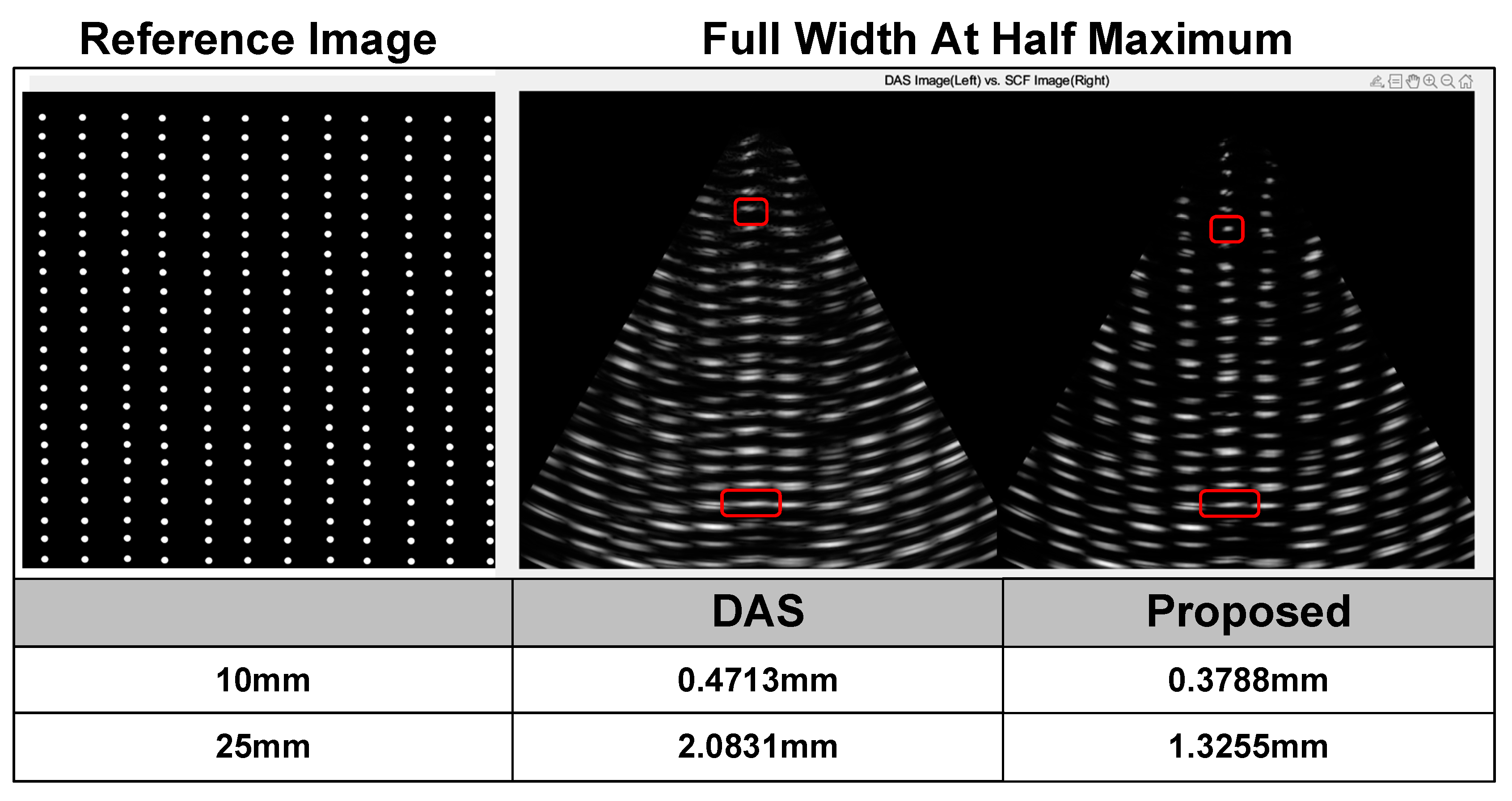
Figure 18 shows the outcomes obtained after measuring the lateral resolution of each focus using the reference image. We assess the lateral resolution at depths of 10 mm and 25 mm, respectively. Our results demonstrate that the lateral resolution of the focus improves by more than 20% at all depths. This indicates that the proposed SCF can achieve a relatively good lateral resolution even for images at close depths.
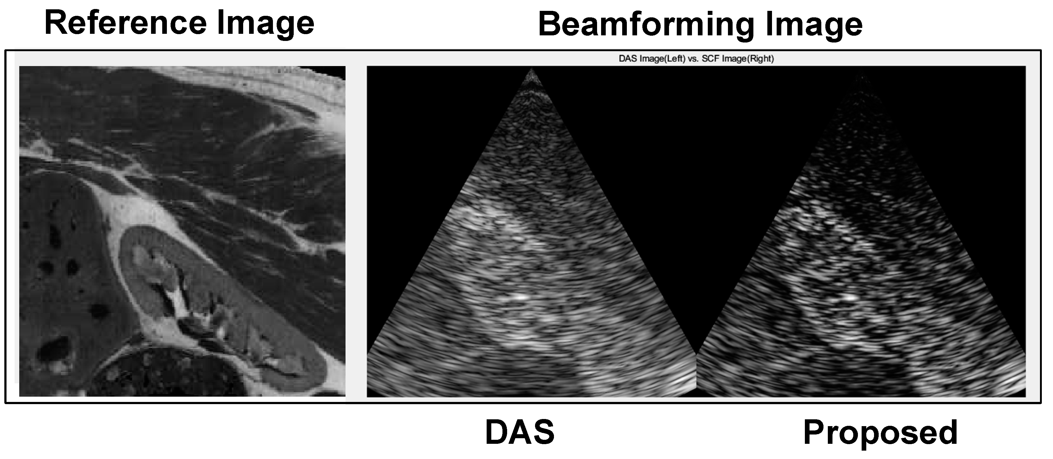
Figure 19 shows the reconstructed image when a reference image is a kidney. The image on the proposed CF is better at distinguishing the boundaries of the tissues when a more complicated image is fed in.
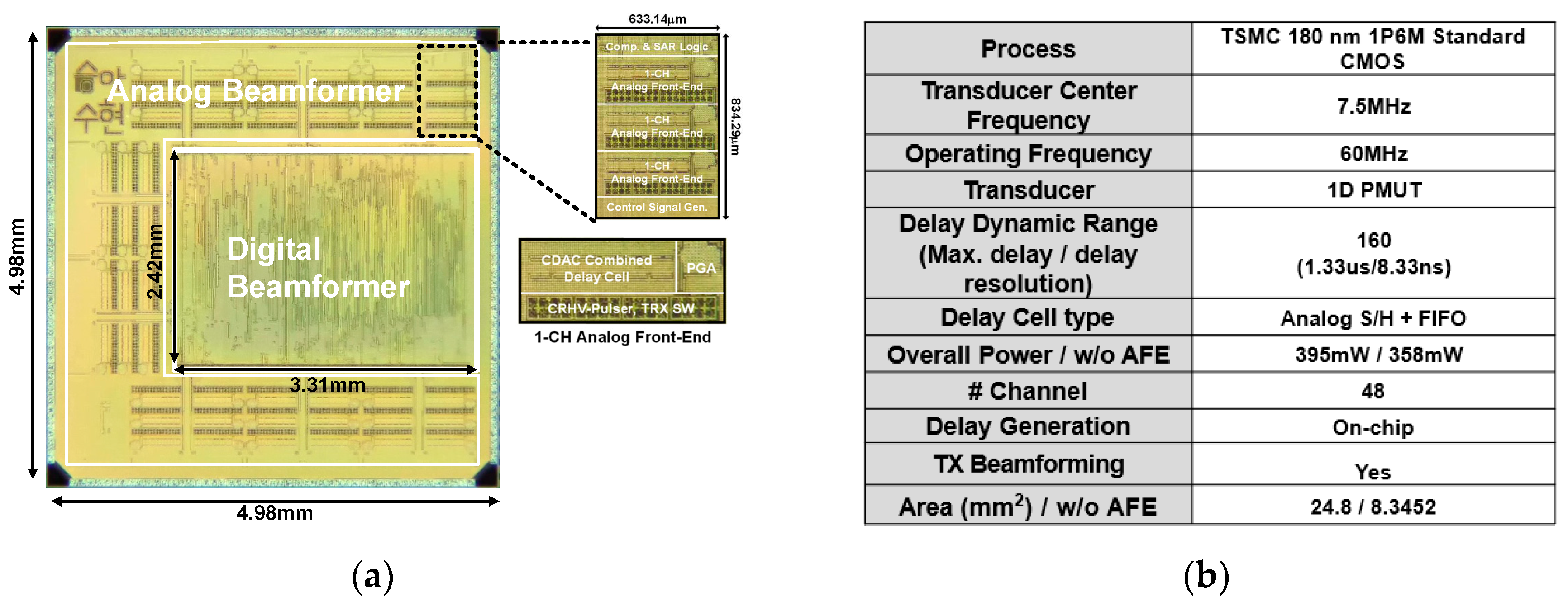
Figure 20 (a) is a micrograph of the implemented ASIC. The chip area is 4.98mm x 4.98mm with 2.42mm x 3.31mm for the digital beamformer and 633.14um x 834.29um for the three channels of the analog beamformer.
Figure 20 (b) summarizes the performance of the chip.
Table 3 presents a comparison of on-chip delay generation for ultrasound beamformers, highlighting the proposed ASIC's unique advantage in minimizing circuit complexity and footprint. The proposed work eliminates memory and LUT usage, leading to a significantly smaller silicon footprint compared to [
8]'s LUT-based implementation (49 focal points, insufficient for high-resolution imaging). Furthermore, [
9]'s off-chip approach incurs greater area overhead. These factors combined demonstrate the proposed ASIC's significant area advantage.
Figure 21.
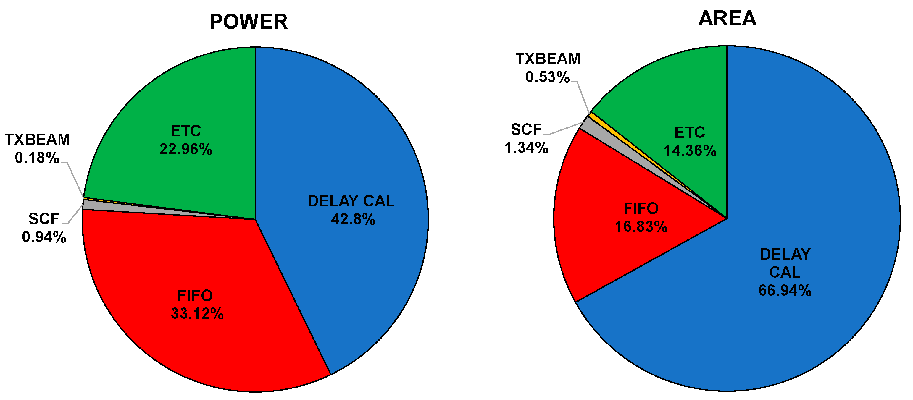
Breakdown of the Power and Area Consumption in ASIC.
Figure 21.
Breakdown of the Power and Area Consumption in ASIC.
5. Discussion with Further Work
The current system requires one TOF calculator per channel in the transducer. As a result, the digital beamformer’s power and area are significantly impacted by the number of calculators. To optimize the power and area efficiency, reducing the number of calculators is recommended. One way to achieve this is by implementing a small number of calculators using time division instead of one calculator per channel. This approach can help maximize power and area savings while maintaining the same number of channels.
In
Figure 22, it is demonstrated that implementing a Time Division Multiplexing (TDM) based delay generator can decrease the frequency at which the delay is updated. However, for the current application, the delay of one channel of a single scan line changes only slightly every two to three sampling points. This implies that depending on the required application, adjusting the degree to which the current structure is time-sliced can be executed more efficiently.
The results of the gate-level synthesis are presented in
Table 4. We changed the delay update interval from 1 clock to 48 clock using the TDM-based delay generator. As a result, the area was reduced to 35.8% from 6.76 mm² to 2.42 mm². Furthermore, the power consumption of the TDM structure was also reduced to 58.57%, indicating that an efficient low-area and low-power implementation is feasible. These findings suggest that the structure has the potential for use in catheter applications that require a small area and for 3D applications that require a large number of channels.
6. Conclusions
This paper presents a mixed-signal ultrasound beamformer ASIC for 48-channel ultrasound endoscopy applications, featuring integrated transmit and receive functionalities to achieve high-resolution image acquisition with reduced power and area consumption. To achieve this, we propose three key design innovations: a charge redistribution-based CRHV pulser generating low-power three-level pulses, a sub-array RX beamformer with a memoryless delay generator for minimal per-channel area, and a hardware-friendly SCF algorithm enabling high-resolution imaging with superior power-to-area efficiency and reduced computational complexity. Consequently, our system surpasses conventional DAS algorithms in image quality while achieving significant power and area savings compared to prior works. Its compact design and efficient operation hold promise for advanced applications in 3D ultrasound imaging and catheterization.
Author Contributions
Conceptualization, Soohyun Yun, Seungah Lee and Joonsung Bae; Methodology, Soohyun Yun and Seungah Lee; Writing – original draft, Soohyun Yun; Writing – review & editing, Joonsung Bae.
Funding
This work was supported by Korea Institute for Advancement of Technology (KIAT) grant funded by the Korea Government (MOTIE) and This work is supported by the Technology Innovation Program under Grant 20012355 (Fully Implantable Closed Loop Brain to X for Voice Communication) funded By the Ministry of Trade, Industry & Energy (MOTIE).
Data Availability Statement
Not applicable.
Conflicts of Interest
The authors declare no conflict of interest.
References
- https://www.cancer.go.kr/.
- Zhong L, Yao QY, Li L, Xu JR. Imaging diagnosis of pancreato-biliary diseases: A control study. World J Gastroenterol 2003; 9(12): 2824-2827. [CrossRef]
- https://www.cancer.gov/about-cancer/diagnosis-staging/diagnosis.
- Catherine, F. Vozzo DO and Madhusudhan R. Sanaka MD., Endoscopic Management of Pancreaticobiliary Disease, Surgical Clinics of North America, The, 2020-12-01, Volume 100, Issue 6, Pages 1151-1168. [CrossRef]
- M. Sautto.; D. Leone.; A. Savoia.; D. Ghisu.; F. Quaglia.; G. Caliano.; A. Mazzanti. A CMUT transceiver front-end with 100-V TX driver and 1-mW low-noise capacitive feedback RX amplifier in BCD-SOI technology, ESSCIRC 2014 - 40th European Solid State Circuits Conference (ESSCIRC), September 2014. [CrossRef]
- Mingliang Tan.; Eunchul Kang.; Jae-Sung An.; Zu-Yao Chang.; Philippe Vince.; Nicolas Sénégond.; Michiel A. P. Pertijs. An Integrated Programmable High-Voltage Bipolar Pulser With Embedded Transmit/Receive Switch for Miniature Ultrasound Probes, IEEE Solid-State Circuits Letters, vol. 2, no. 9, September 2019, pp. 79-82. [CrossRef]
- Kailiang Chen.; Hae-Seung Lee.; Charles G. Sodini. A Column-Row-Parallel ASIC Architecture for 3-D Portable Medical Ultrasonic Imaging, IEEE Journal of Solid-State Circuits, vol. 51, no. 3, March 2016, pp. 738-751. 20 March. [CrossRef]
- Jihee Lee.; Kyoung-Rog Lee.; Benjamin E. Eovino.; Jeong Hoan Park.; Luna Yue Liang.; Liwei Lin.; Hoi-Jun Yoo.; Jeral Yoo. A 36-Channel Auto-Calibrated Front-End ASIC for a pMUT-Based Miniaturized 3-D Ultrasound System, IEEE Journal of Solid-State Circuits, Volume: 56, Issue: 6, June 2021, pp. 1910-1923. [CrossRef]
- Ji-Yong Um.; Yoon-Jee Kim.; Seong-Eun Cho.; Min-Kyun Chae.; Jongkeun Song.; Baehyung Kim.; Seunghun Lee.; Jihoon Bang.; Youngil Kim.; Kyungil Cho.; Byungsub Kim.; Jae-Yoon Sim.; Hong-June Park. An Analog-Digital Hybrid RX Beamformer Chip With Non-Uniform Sampling for Ultrasound Medical Imaging With 2D CMUT Array, IEEE Transactions on Biomedical Circuits and Systems, Volume: 8, Issue: 6, December 2014, pp. 799-809. [CrossRef]
- Yoon-Jee Kim.; Sung-Eun Cho.; Ji-Yong Um.; Min-Kyun Chae.; Jihoon Bang.; Jongkeun Song.; Taeho Jeon.; Byungsub Kim.; Jae-Yoon Sim.; Hong-June Park. A Single-Chip 64-Channel Ultrasound RX-Beamformer Including Analog Front-End and an LUT for Non-Uniform ADC-Sample-Clock Generation, IEEE Transactions on Biomedical Circuits and Systems, Volume: 11, Issue: 1, February 2017, pp. 87-97. [CrossRef]
- Chang-Hong Hu.; Xiao-Chen Xu.; Jonathan M Cannata.; Jesse T Yen, K Kirk Shung.; Development of a real-time, high-frequency ultrasound digital beamformer for high-frequency linear array transducers, IEEE Trans Ultrason Ferroelectr Freq Control. 2006 Feb;53(2), pp. 317-323. [CrossRef]
- M. Almekkawy.; Jingwei Xu.; Mohan Chirala. An optimized ultrasound digital beamformer with dynamic forcusing implemented on FPGA, IEEE Eng. Medicine Biol. Soc., Aug. 2014, pp. 3296–3299. [CrossRef]
- Ji-Yong Um.; Yoon-Jee Kim.; Seong-Eun Cho.; Min-Kyun Chae.; Byungsub Kim.; Jae-Yoon Sim.; Hong-June Park. A single-chip 32-channel analog beamformer with 4-ns delay resolution and 768-ns maximum delay range for ultrasound medical imaging with a linear array transducer, IEEE Trans. Biomed. Circuits Syst., vol. 9, no. 1, Feb. 2015, pp 138–151. [CrossRef]
- Liuhao Wu., Jiaqi Guo., Rucheng Jiang., Yande Peng., Han Wu., Jiamin Li., Yang Luo., Liwei Lin., Jerald Yoo.,"An Ultrasound Imaging System With On-Chip Per-Voxel RX Beamfocusing for Real-Time Drone Applications", IEEE Journal of Solid-State Circuits, Volume: 57, Issue: 11, November 2022, pp. 3186-3199. [CrossRef]
- Aya Ibrahim.; Shuping Zhang.; Federico Angiolini.; Marcel Arditi.; Shinji Kimura.; Satoshi Goto.; Jean-Philippe Thiran.; Giovanni De Micheli.; Towards Ultrasound Everywhere A Portable 3D Digital Back-End Capable of Zone and Compound Imaging, IEEE Transactions on Biomedical Circuits and Systems, Volume: 12, Issue: 5, October 2018, pp. 968-981. [CrossRef]
- Jeeun Kang.; Pilsu Kim.; Changhan Yoon.; Yangmo Yoo.; Tai-Kyong Song.; Efficient Parallel-Beamforming Based on Shared FIFO for Ultra-Compact Ultrasound Imaging Systems, IEEE Access, Volume: 8, pp. 80490-80501. [CrossRef]
- Mayur Agarwal.; Abhishek Tomar.; Navneet Kumar.; An IEEE single-precision arithmetic based beamformer architecture for phased array ultrasound imaging system, Engineering Science and Technology, an International Journal Volume 24, Issue 5, October 2021, pp. 1080-1089. [CrossRef]
- Aya Ibrahim.; Pascal A. Hager.; Andrea Bartolini.; Federico Angiolini.; Marcel Arditi.; Jean-Philippe Thiran.; Luca Benini.; G. De Micheli. Efficient Sample Delay Calculation for 2-D and 3-D Ultrasound Imaging, IEEE Transactions on Biomedical Circuits and Systems, Volume: 11, Issue: 4, August 2017, pp. 815-831. [CrossRef]
- Jian-Yu, Lu.; Hehong, Zou.; James, F.Greenleaf. Biomedical Ultrasound beam forming, Ultrasound in Medicine & Biology Volume 20, Issue 5, 1994, pp. 403-428. [CrossRef]
- Giulia Matrone.; Alessandro Stuart Savoia.; Giosuè Caliano.; Giovanni Magenes. The Delay Multiply and Sum Beamforming Algorithm in Ultrasound B-Mode Medical Imaging, IEEE Transactions on Medical Imaging, Volume: 34, Issue: 4, April 2015, pp. 940-949. [CrossRef]
- Seungwan Jeon.; Eun-Yeong Park.; Wonseok Choi.; Ravi Managuli.; Ki jong Lee.; Chulhong Kim. Real-time delay-multiply-and-sum Beamforming with coherence factor for in vivo clinical photoacoustic imaging of humans, Photoacoustics Volume 15, September 2019, 100136. [CrossRef]
- Seungah Lee.; Soohyun Yun.; Joonsung Bae. A low-power and area-efficient ultrasound receiver using beamforming successive approximation register analog-to-digital converter with capacitive digital-to-analog converter combined delay cell structure for 3-D imaging systems, Electronics Letters Volume 58, Issue 22, Oct 2022, pp. 819-855. [CrossRef]
- K.W. Hollman., K.W. Rigby., M. O'Donnell., Coherence factor of speckle from a multi-row probe, 1999 IEEE Ultrasonics Symposium. Proceedings. International Symposium, 17-20 October 1999. [CrossRef]
- T. L. Szabo. Diagnostic ultrasound imaging: inside out, Academic Press, 2004.
- Bradley E Treeby.; B T Cox.; k-Wave: MATLAB toolbox for the simulation and reconstruction of photoacoustic wave fields, Journal of Biomedical Optics, Vol. 15, Issue 2, March 2010, 021314.
- Li Li.; Xinliang Yu.; Fangqin Li.; Baojia Chen. Parameter Optimization of Linear Phased Array Transducer for Defect Detection, The Open Automation and Control Systems Journal, 2014, 6, pp. 488-492.
- Rais Ahmad.; Tribikram Kundu.; Modeling of phased array transducers, The Journal of the Acoustical Society of America, Volume 117, Issue 4, May 2005, pp. 1762-1776. [CrossRef]
- J.A. Jensen. Field: A Program for Simulating Ultrasound Systems, Medical & Biological Engineering & Computing, Volume 34, Supplement 1, January 1996, pp. 351-353.
Figure 1.
Pancreaticobiliary Ultrasound Endoscopy System.
Figure 1.
Pancreaticobiliary Ultrasound Endoscopy System.
Figure 2.
Conventional TX Pulsers.
Figure 2.
Conventional TX Pulsers.
Figure 3.
(a) Conventional LUT-based RX Beamformer. (b) Conventional Calculator-based RX Beamformer.
Figure 3.
(a) Conventional LUT-based RX Beamformer. (b) Conventional Calculator-based RX Beamformer.
Figure 4.
Conventional Beamforming Algorithms for High Image Resolution. (a) Delay Multiply and Sum. (b) Coherence Factor Delay and Sum.
Figure 4.
Conventional Beamforming Algorithms for High Image Resolution. (a) Delay Multiply and Sum. (b) Coherence Factor Delay and Sum.
Figure 5.
Block Diagram of Overall System.
Figure 5.
Block Diagram of Overall System.
Figure 6.
CRHV TX Pulser Block.
Figure 6.
CRHV TX Pulser Block.
Figure 7.
Charge Redistribution 3-level HV Pulser.
Figure 7.
Charge Redistribution 3-level HV Pulser.
Figure 8.
Block Diagram of the Proposed Delay Generator.
Figure 8.
Block Diagram of the Proposed Delay Generator.
Figure 9.
Memoryless Structure using RX Enable Signal for the RX Beamformer.
Figure 9.
Memoryless Structure using RX Enable Signal for the RX Beamformer.
Figure 10.
3-Channel Analog Subarray Beamforming Architecture
Figure 10.
3-Channel Analog Subarray Beamforming Architecture
Figure 11.
Analog Subarray Beamforming Control Signals.
Figure 11.
Analog Subarray Beamforming Control Signals.
Figure 12.
Block Diagram of the Digital RX Beamformer.
Figure 12.
Block Diagram of the Digital RX Beamformer.
Figure 13.
Block Diagram of the SCF Processor.
Figure 13.
Block Diagram of the SCF Processor.
Figure 14.
Measurement Results of (a) TX Output Pulses (b) Dynamic Power Loss.
Figure 14.
Measurement Results of (a) TX Output Pulses (b) Dynamic Power Loss.
Figure 15.
Lateral Resolution Comparison among Conventional and Proposed Algorithms.
Figure 15.
Lateral Resolution Comparison among Conventional and Proposed Algorithms.
Figure 16.
Contrast Ratio Comparison among Conventional and Proposed Algorithms.
Figure 16.
Contrast Ratio Comparison among Conventional and Proposed Algorithms.
Figure 17.
Contrast Ratio Comparison Results using ASIC.
Figure 17.
Contrast Ratio Comparison Results using ASIC.
Figure 18.
Lateral Resolution Comparison Results using ASIC.
Figure 18.
Lateral Resolution Comparison Results using ASIC.
Figure 19.
Comparison of Kidney Image Results using ASIC.
Figure 19.
Comparison of Kidney Image Results using ASIC.
Figure 20.
(a) Chip Micrograph and (b) Performance Summary.
Figure 20.
(a) Chip Micrograph and (b) Performance Summary.
Figure 22.
Implementing a TDM-Delay Generator.
Figure 22.
Implementing a TDM-Delay Generator.
Table 1.
Artix-7 XC7a100tcsg324 Synthesis Utilization Result.
Table 1.
Artix-7 XC7a100tcsg324 Synthesis Utilization Result.
| Beamforming Algorithm |
Channels |
Logic LUTs |
Memory LUTs |
Regs |
BRAM |
DSP |
| Delay and Sum * |
16 |
36.27% |
0.51% |
22.91% |
0 |
26.67% |
| Single Precision Coherence Factor |
16 |
51.14% |
0.51% |
23.30% |
0 |
57.08% |
| Shift Coherence Factor |
16 |
39.21% |
0.51% |
23.22% |
0 |
27.08% |
Table 2.
Artix-7 XC7a100tcsg324 Synthesis Power Result.
Table 2.
Artix-7 XC7a100tcsg324 Synthesis Power Result.
| Beamforming Algorithm |
ALL |
ETC |
Delay Generator |
FIFO |
CF |
| Delay and Sum * |
483.080W
(100%) |
25.309W
(5.2%) |
359.546W
(74.4%) |
98.495W
(20.4%) |
0W
(0%) |
| Single Precision Coherence Factor |
689.602W
(100%) |
20.668W
(3%) |
357.116W
(51.8%) |
113.407W
(16.4%) |
198.411W
(28.8%) |
| Shift Coherence Factor |
522.020W
(100%) |
27.404W
(5.3%) |
353.826W
(67.8%( |
112.823W
(21.6%) |
27.967W
(5.3%) |
Table 3.
Performance Comparison Table.
Table 3.
Performance Comparison Table.
| |
This Work |
JSSC2022[14] |
ISSCC2019[8] |
TBCAS2017[10] |
TBCAS2014[9] |
| Process |
180nm |
180nm |
180nm |
130nm |
130nm |
| Center Frequency |
Standard
CMOS
|
Standard
CMOS |
Standard
CMOS |
Standard
CMOS |
Standard
CMOS |
Delay Dynamic Range
(Max. delay / delay resolution) |
160
(1.33us/8.33ns)
|
N/A |
256
(1.28us/5ns) |
1260
(7.875us/6.25ns) |
1280
(8us/6.25ns) |
| Memory Usage |
X |
SRAM |
X |
X |
X |
| Delay cell type |
Analog S/H
+ FIFO
|
Memory |
Analog S/H |
FIFO |
Analog S/H
+ FIFO |
| Overall Power |
395mW |
142.3mW |
371.88mW |
605mW |
1.14W |
| # Channel |
48 |
64 |
36 |
64 |
64 |
Delay Generation
(Method) |
On-chip
(Calculation)
|
On-chip
(Calculation) |
On-chip
(LUT) |
On-chip
(LUT) |
Off-chip |
| TX Beamforming |
O |
O |
O |
X |
X |
| Area (mm2) |
24.8 |
32.5 |
11.75 |
30.25 |
19.4 |
Table 4.
Design Compiler Synthesis Result.
Table 4.
Design Compiler Synthesis Result.
| Beamformer Architecture |
Area |
Power |
Cell Count |
| Digital Beamformer |
6.76mm2
|
358mW |
270317 |
| TDM Digital Beamformer |
2.42mm2
|
226mW |
84772 |
|
Disclaimer/Publisher’s Note: The statements, opinions and data contained in all publications are solely those of the individual author(s) and contributor(s) and not of MDPI and/or the editor(s). MDPI and/or the editor(s) disclaim responsibility for any injury to people or property resulting from any ideas, methods, instructions or products referred to in the content. |
© 2023 by the authors. Licensee MDPI, Basel, Switzerland. This article is an open access article distributed under the terms and conditions of the Creative Commons Attribution (CC BY) license (http://creativecommons.org/licenses/by/4.0/).
