Introduction
Polymers appear very attractive as active layers in OFETs. They have demonstrated a propensity for being low cost [
1,
2], lightweight [
3,
4], flexible, [
5,
6], biocompatible [
7], scalable [
8,
9], and processable at low temperatures.[
10] They have also been demonstrated as the active layer for a variety of applications including sensors[
11,
12] and displays.[
13,
14] Yet, when compared to other organics such as evaporated small molecule active layers, polymer devices are plagued by low mobility, output current, and on-off ratios. Doping can greatly enhance the electrical characteristics of such polymer devices and can provide further insight into charge carrier generation and transport.[
15]
Doping of organic field-effect transistors is the subject of numerous reports including that of Wang et al. who investigated the benefits of weak dopants on a P3HT host [
16], Hu et al. who investigated n-type doping and worked within the strong electron donating properties of the species, DBU [
17], Ma et al. who doped P3HT with small quantities of F4-TCNQ and investigated the impact of charge-transfer complexes on the output and transfer characteristics of that system [
18], and Thomas et al. who looked at the impact of ions on the polymer microstructure and density-of-states functions.[
19] In a similar fashion, modulation of the Seebeck coefficient with gate voltage has been investigated by Venkatenhvaran et al. with the p-type polymer semiconductor PBTTT[
20], Pernstich et al. who investigated both the temperature-dependent thermopower and carrier density-dependent thermopower in rubrene and pentacene small molecules[
21], Warwick et al. who reviewed high mobility small molecules using an on-chip architecture[
22], and by Zhang et al. who investigated the ability to predict the outcomes of chemical doping by measuring the gate voltage impact on the thermoelectric properties of a series of polymers.[
23] Modulation of the Seebeck coefficient, however, has not been reported on the same device as thermal modulation for a doped organic semiconductor (OSC) active layer.
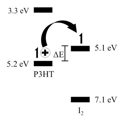
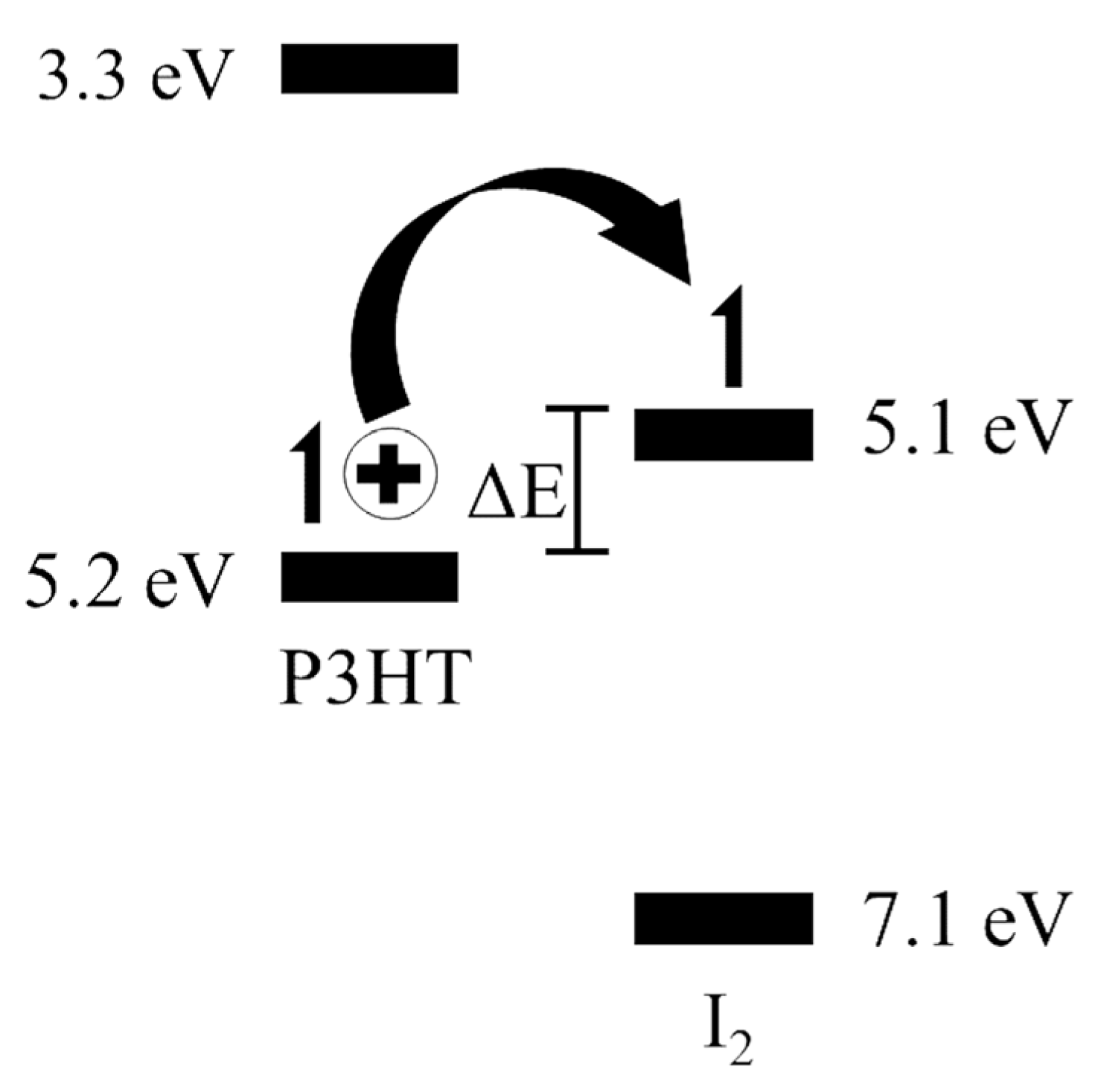
In this study, a series of undoped and iodine-doped OFETs with dopant concentrations below 1.0% mole ratio are first evaluated in order to find the location of the maximum on-off ratio and apparent device mobility. This binary composite system, its frontier orbitals, and energy offset are depicted in
Figure 1. Then, a series of long channel OFETs are fabricated to demonstrate a dual-modulation field-effect device whereby temperature can modulate the properties of the field-effect transistor and gate voltage can modulate the properties of the organic thermoelectric system.[32-34] Observed trends may aid in better understanding the role of thermoelectric dopants in charge generation and separation such as the P3HT-iodine binary system.
Experimental
Materials
Heavily-doped n-type silicon wafers were procured with a 300 nm dry thermally oxidized SiO2 layer and diced to a size of 15 mm x 20 mm by the fabricator. These diced wafers were utilized as the substrates for all devices. Regioregular P3HT (Reike Metals via Sigma Aldrich, SKU: 445703) and iodine (Alfa Aesar, SKU: 00158), were used for the active layer of the OFET and octadecyltrichlorosilane (OTS) (Merck, SKU: 8.22170.0100) was used as a self-assembled monolayer to modify the surface of the SiO2 gate dielectric. The binary composite P3HT and iodine system was dissolved in ortho-dichlolobenzene (o-DCB) and anhydrous toluene was the diluent for the OTS. All chemicals and solvents were used as provided from the manufacturers without further purification.
Solution and Device Fabrication
Stock solutions of P3HT in o-DCB were made at a concentration of 16 mg/mL and stock solutions of iodine in o-DCB were made at 2 % mole ratio with respect to the final blended P3HT concentration of 8 mg/mL. Those stock solutions were then stirred overnight for a minimum of 8 hours. After stirring, 8 mg/mL P3HT aliquots were doped with iodine via solution doping at 0.1%, 0.25%, 0.5%, and 1.0% mole ratio with an undoped P3HT aliquot also produced. These were used for an initial broad determination of an optimal doping concentration. The second doping series presented herein utilized the same solution procedure as above, but only undoped, 0.25% and 0.5% mole ratio solutions were produced and were used for dual-modulation devices. The diced Si/SiO
2 substrates were cleaned by immersion in an ultrasonic bath first with acetone and then with isopropanol for 30 minutes each before drying with a dry nitrogen stream. Source, drain, and gate contacts were thermally evaporated through a shadow mask by first depositing a 2 nm Cr adhesion promotion layer at a rate of 0.5 Å/s followed by a 50 nm Au layer at an average rate of 1.5 Å/s. For the broader doping concentration study (undoped – 1%), devices have a channel length of 60 µm and a channel width of 1 mm. For the dual modulation study, one device was produced on each substrate with a channel length of 0.580 mm and a channel width of 12 mm. After evaporation, devices were exposed to oxygen plasma for 30 s. SiO
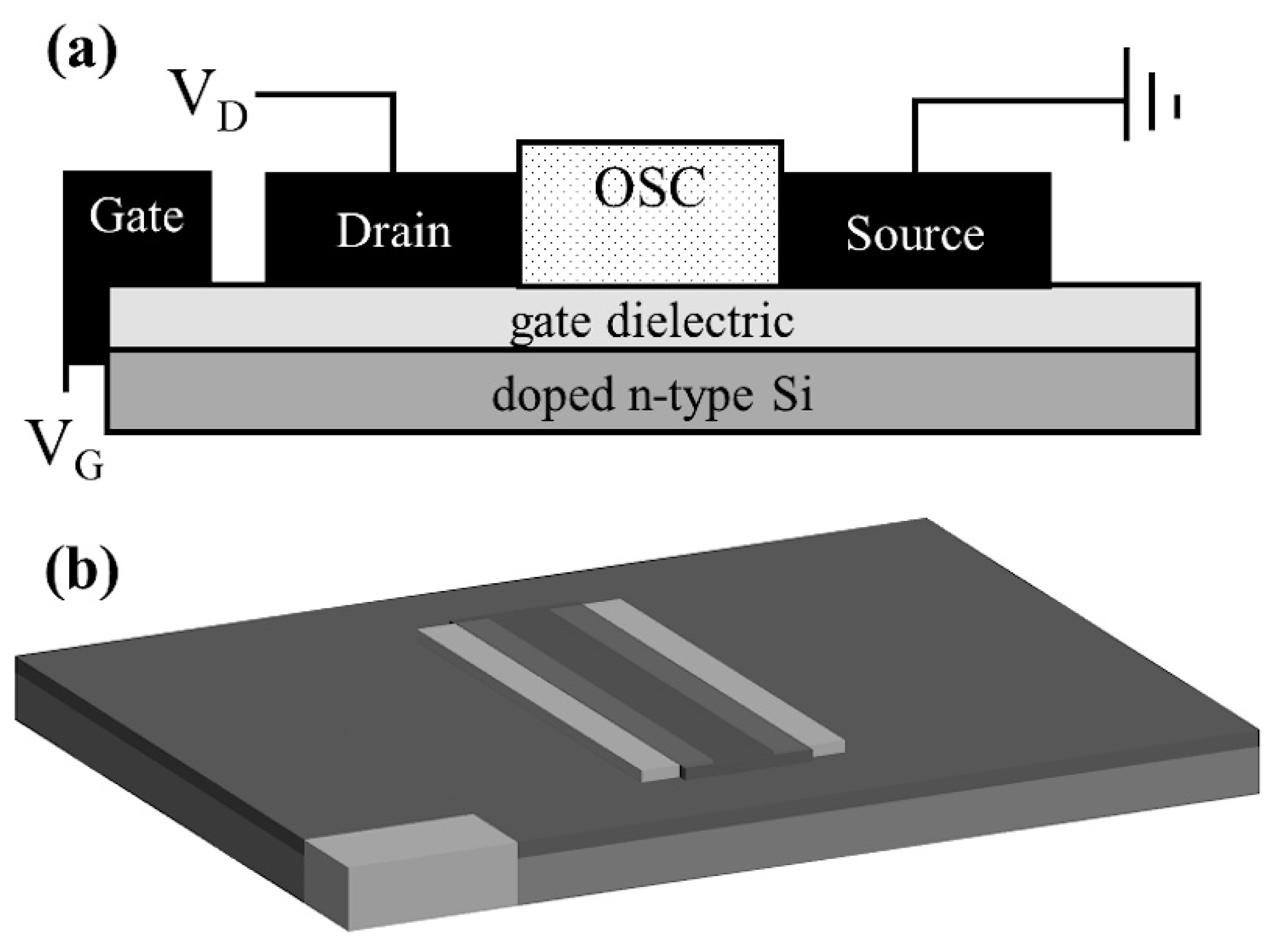
2 gate dielectric surfaces were then treated with OTS in anhydrous toluene by immersion for 30 minutes followed by a cyclohexane rinse and then dried in a dry nitrogen stream. Thin film active layers were deposited via spin coating at 1500 rpm for 120 s before being dried overnight in a vacuum oven at 80 °C to produce active layers with thicknesses of 26 nm on average. Finished devices were of the bottom-gate bottom-contact (BGBC) coplanar configuration as shown in both
Figure 2(a) and
Figure 2(b).
Output and Transfer Characterization
Characterization of the devices’ field-effect attributes was performed with a Keithley 4200-SCS semiconductor analyzer and Signatone 1160 probe station in atmosphere. Uniform heating of the devices was accomplished with a TETech plate cooler controlled with a TE-720 Thermoelectric Temperature controller. Temperature on the surfaces of the devices was verified via contact and with a FLIR A300 series IR imaging camera. Samples were stabilized at the reported temperature for a minimum of 5 minutes prior to data collection. Transfer curves were averaged from both forward and reverse sweeps through the presented range of voltages.
Seebeck Coefficient Characterization
Characterization of the active layers’ thermoelectric properties was performed with a Keithley 4200-SCS semiconductor analyzer and Signatone 1160 probe station in atmosphere. Au probe tips were used to contact the Au source and drain contacts for voltage measurement. A temperature gradient across the OFET channel was achieved through the use of two TETech plate coolers, each connected to a TE-720 thermoelectric temperature controller. Temperature across the channel was verified with a FLIR A300 series IR imaging camera and by contact. Samples were stabilized at the planned temperature gradient for five minutes prior to any data acquisition.
Atomic Force Microscopy
The surface morphology of the active layers was characterized using a Bruker Veeco Dimension XT atomic force microscope set to tapping mode in air. A 5µm x 5µm scanning area was used in the channel of each of the devices and samples were first evaluated following fabrication and prior to any electrical characterization. The morphology was again evaluated following seebeck, output, and transfer characterization in a location as close to the original scan area as possible. All height images were processed using the same methodology and exported so maximum heights were presented on the same scale. Roughness values were calculated from flattened images after processing.
Results and Discussion
Optimization of Doping Concentration Range
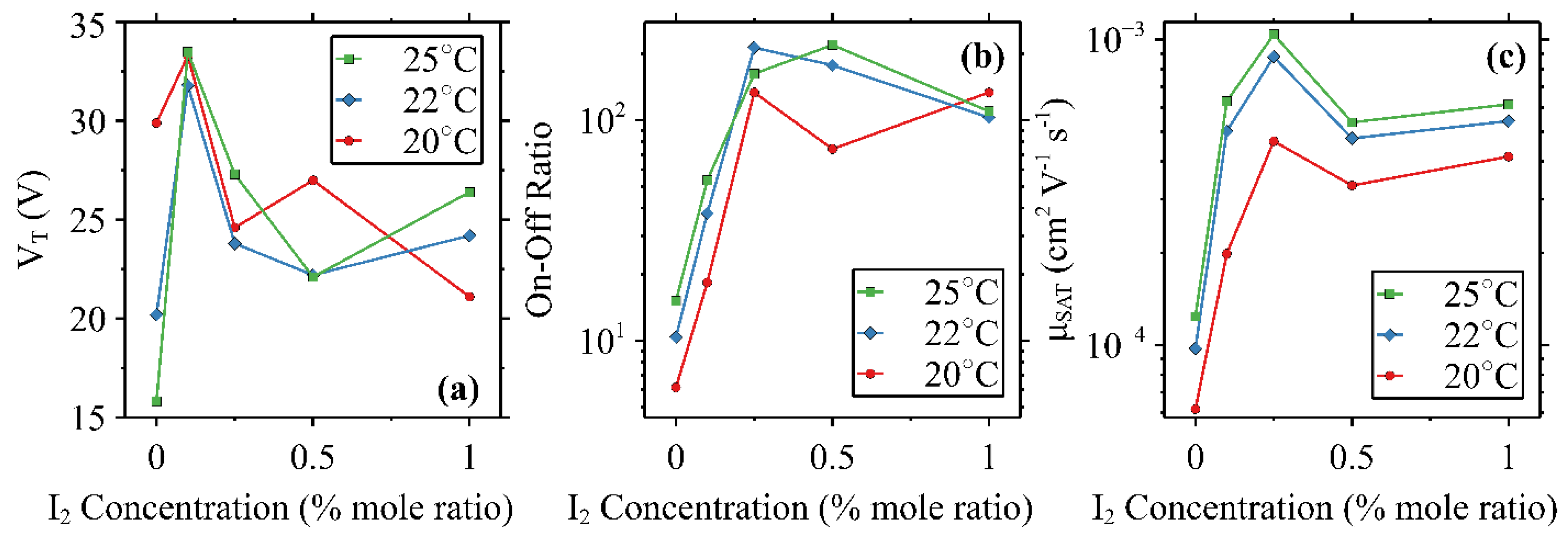
The objective of the screening test at dopant concentrations below 1.0% mole ratio was to find the maximum on-off ratio and pursue further characterization of both field-effect modulation and thermoelectric property modulation within that range. Parameters extracted from the transfer curves taken in the saturation region (V
DS = -60 V) at 20 °C, 22 °C, and 25 °C are presented in
Figure 3. The 0.1% device exhibited the greatest threshold voltage (V
T) at all temperatures and is displayed in
Figure 3(a).As can be seen from the on-off ratios in
Figure 3(b), a maximum of 2.14x10
2 is observed for the 0.25% device at 22 °C and a maximum of 2.20x10
2 is observed for the 0.25% device at 25 °C. These values are within the expected range of comparable P3HT-based devices which can vary over several orders of magnitude depending on the concentration [
24] or gate dielectric.[
25] Saturated device mobility values are presented in
Figure 3(c), and, similarly, exhibit maximums for each of the three tested temperatures for the 0.25% sample. The apparent device mobility (also called FET mobility) increases with temperature in both undoped and iodine-doped devices, as expected for temperature-dependent mobility behavior as well as thermoelectric doping generated charges.[
26,
27] A slight dip at all temperatures for the 0.5% samples suggests further investigation may be necessary to further understand the impact of iodine doping on the mobility of the P3HT and iodine binary system. Previous work with a P3HT, iodine, and PCBM ternary dual-functional photoelectric-thermoelectric system revealed a peak conversion efficiency in samples doped with 5% mole ratio iodine[
28], but the primary direction of charge transport differs between those reported solar cell devices (z-axis) and the OFETs reported here (x-y plane). The general trend downward at 1% for both on-off ratio and mobility suggests further focus of this study should be directed toward doping concentrations of 0.25% and 0.5%.
Thermal Modulation of the dual-modulation OFET
Output and transfer characteristics in saturation (V
DS = -60 V) for devices on which dual-modulation is exhibited are displayed in
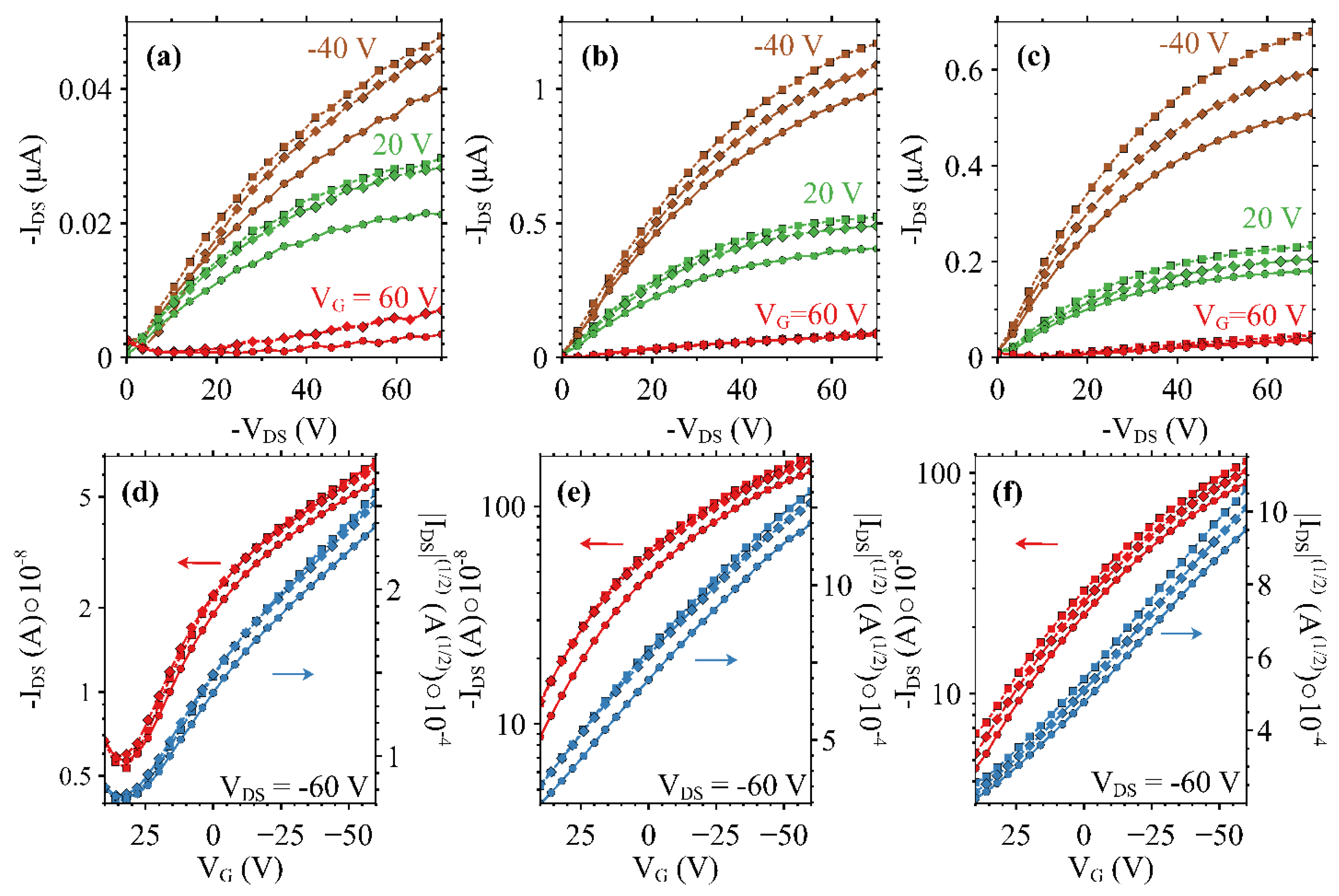
Figure 4. Output curves for three uniform surface temperatures (20 °C, 22 °C, and 25 °C) are presented in
Figure 4(a-c) while transfer curves at the same three temperatures are presented in Figure 4(d-f). A increase in conductivity is expected as temperature is increased due to the incoherent charge transport which is dominant in disordered soft materials.[
29,
30] The addition of iodine in the doped samples acts as an electron trap as temperature is increased which provides additional free holes available to move through the HOMO of the P3HT. Both iodine-doped devices outperform their undoped counterpart by at least a factor of 10 over the same range of gate voltages. The 0.25% iodine-doped device exhibited the greatest output current of the three devices, reaching into the microampere range in saturation at 22 °C, and 25 °C at a V
G = -40 V. Transfer curves of the doped devices exhibit a well-defined linear slope from which the values of
Table 1 were calculated. A maximum on-off ration of 3.91x10
1 is observed for the 0.25% device at 25 °C, and the on-off ratios of both doped devices exceeded those of the the undoped device at all tested temperatures. The presented on-off ratios may be underestimated due to a truncated range over which the test was executed out of an abundance of caution to prevent damage during characterization.
Gate Voltage Modulation of the Thermoelectric Properties
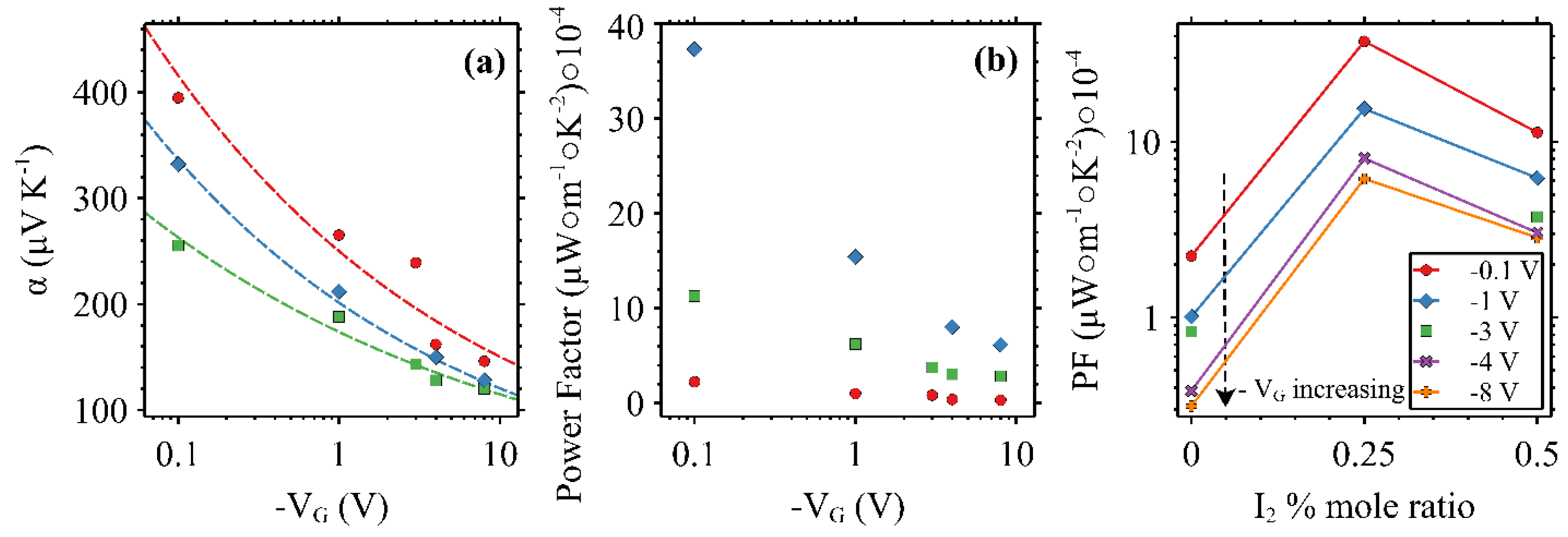
Modulation of the thermoelectric properties for each of the three devices with channel lengths of 580 µm is presented in
Figure 5(a-c). Each point presented in
Figure 5(a) represents a slope calculated from a series of three measurements at three different temperature gradients created across the source and drain contacts of the OFET according to the equation,
. As gate voltage is increased (to the negative for p-type transport) a decrease is observed in the Seebeck coefficient for both undoped and doped devices. Likewise, as doping concentration is increased, a decrease in the Seebeck coefficient is observed for devices tested at the same gate voltage. Thermoelectric power factor vs. gate voltage is presented in
Figure 5(b) and is calculated following the equation
using values interpolated from the range of gate voltages over which the output curves were acquired at 20 °C. A maximum value of 3.7x10
-3 µW·m
-1·K
-2 at -0.1 V was observed in the 0.25% iodine-doped device with the 0.25% exhibiting the greatest power factor across the tested voltage range. The 0.5% sample had the second highest values followed by the undoped device.
Figure 5(c) additionally presents the thermoelectric power factor with respect to the conductivities of each of the three devices. It can be seen from both
Figure 5(b) and
Figure 5(c) the significance of the doping-induced conductivity gains on the thermoelectric power factor and performance of these OFETs compared to that of the undoped device. We posit that the primary driver for the increase in conductivity of the system upon heating is due to the increased number of charge carriers with both an increase in doping concentration and an increase in gate voltage. Per the long-form equation for the Seebeck coefficient,
, the number of charge carriers in the system is inversely proportional to the Seebeck coefficient. So while the undoped sample may have the greater Seebeck coefficient of the samples tested, the 0.25%, and to a lesser degree, the 0.5% iodine-doped sample, have the greater thermoelectric power factors. It is expected that a maximum power factor can be found at some gate voltage less that those presented here and may be cause for further work due to the trade off between the seebeck coefficient’s inverse proportionality to the power factor and the conductivity’s direct proportionality.[
31]
Atomic Force Microscopy
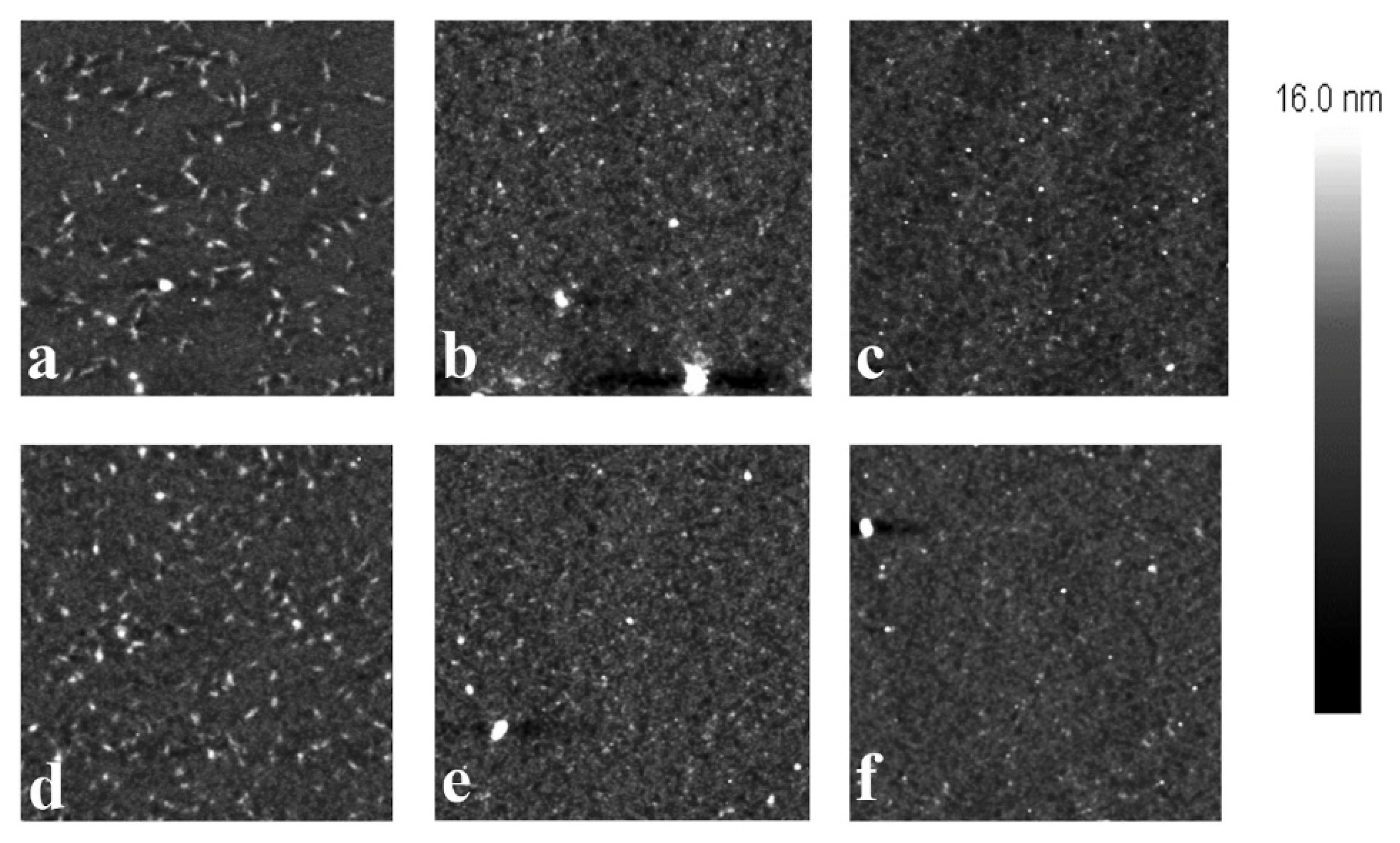
To understand the impacts of the high voltage from electrical characterization and heating on the microstructure, AFM imagery was captured before and after seebeck, output, and transfer curves were acquired. AFM images are shown in
Figure 6 where the top row (Figure (6)(a-c)) was taken before any other characterization and the bottom row (
Figure 6(d-f)) was taken after seebeck, output, and transfer tests were performed. No significant qualitative changes were observed in the undoped (
Figure 6(a,d)), 0.25% (
Figure 6(b,e)), or 0.5% (
Figure 6(c,f)) iodine-doped. That is, the major visual characteristics of either of the sets of images did not exhibit net increases or decreases in either the size or quantity of the features observed. It should be noted that a direct comparison is difficult to achieve given the scan size of 25 µm
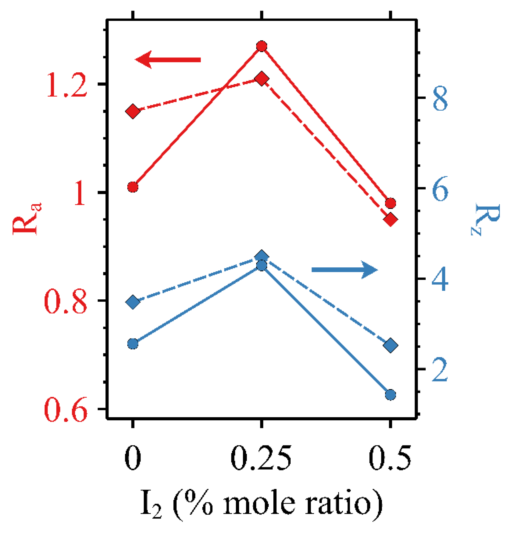
2. A quantitative analysis was performed on the basis on surface roughness, however.
Figure 7 displays the R
a and R
z values for the OFETs with the 0.25% mole ratio iodine-doped specimen exhibiting a greater surface roughness average and range than either of the other two active layers. It has been proposed that this is due to an increase in the degree of halogen bonding present at low concentrations of iodine.[
28]
Conclusions
Undoped and iodine-doped P3HT OFETs were tested at various levels of heat and gate voltage which modulated the field-effect and thermoelectric characteristics, respectively. Doping P3HT with small quantities of iodine around 0.25% mole ratio improved the on-off ratio over that of undoped devices by an order of magnitude and improved the conductivity of all devices compared to that of the undoped device. The seebeck coefficient decreases with respect to both an increase in dopant concentration and gate voltage (negative for p-type), each of which is due to an increase in the charge carrier density present in the active layer. A maximum power factor of 3.7x10⁻³ µW·m-1·K-2 was observed at -0.1 V in the 0.25% sample and overall the 0.25% sample had the highest thermoelectric power factor followed by the 0.5% sample and then undoped sample. AFM imagery revealed that there were no visible permanent changes in the microstructures of any samples due to electrical characterization or changes in temperature.
Data Availability Statement
Additional data including electronic copies of author’s earlier related publications student thesis/dissertations may be available at certain online databases or may be obtained directly from the author or from the library of author’s organization where the student thesis/dissertation hard copies may be housed.
Acknowledgments
The authors wish to express their thanks to Profs. Messaoud Bahoura and Sacharia Albin for the use of laboratories utilized for the characterization of OFETs. This material is based upon work supported, in parts, by research and/or educational grant awards from the National Science Foundation (Award HRD # 1547771 and # 2112595).
Conflicts of Interest
“The authors declare no any conflict of interest.”
References
- Huewe, F.; Steeger, A.; Pflaum, J.; Kostova, K.; Dimitrov, V.; Burroughs, L.; Woodward, S.; Bauer, I.; Strohriegl, P. Low-Cost and Sustainable Organic Thermoelectrics Based on Low-Dimensional Molecular Metals. Adv. Mater. Deerfield Beach Fla 2017. [Google Scholar] [CrossRef] [PubMed]
- Kwon, S.; Kang, H.; Lee, J.-H.; Lee, J.; Hong, S.; Kim, H.; Lee, K. Effect of Processing Additives on Organic Photovoltaics: Recent Progress and Future Prospects. Adv. Energy Mater. 2017, 7, 1601496. [Google Scholar] [CrossRef]
- Richardson, B.; Zhu, L.; Yu, Q. Design and development of plasmonic nanostructured electrodes for ITO-free organic photovoltaic cells on rigid and highly-flexible substrates. Nanotechnology 2017. [Google Scholar] [CrossRef]
- Valimaki, M.; Jansson, E.; Korhonen, P.; Peltoniemi, A.; Rousu, S. Custom-Shaped Organic Photovoltaic Modules-Freedom of Design by Printing. Nanoscale Res. Lett. 2017, 12, 117. [Google Scholar] [CrossRef] [PubMed]
- Park, T.; Park, C.; Kim, B.; Shin, H.; Kim, E. Flexible PEDOT electrodes with large thermoelectric power factors to generate electricity by the touch of fingertips. Energy Environ. Sci. 2013, 6, 788–792. [Google Scholar] [CrossRef]
- Zhang, Q.; Sun, Y.; Xu, W.; Zhu, D. Thermoelectric energy from flexible P3HT films doped with a ferric salt of triflimide anions. Energy Environ. Sci. 2012, 5, 9639–9644. [Google Scholar] [CrossRef]
- Prabavathy, N.; Shalini, S.; Balasundaraprabhu, R.; Velauthapillai, D.; Prasanna, S.; Muthukumarasamy, N. Enhancement in the photostability of natural dyes for dye-sensitized solar cell (DSSC) applications: a review. Int. J. Energy Res. 2017, 41, 1372–1396. [Google Scholar] [CrossRef]
- Lucera, L.; Machui, F.; Schmidt, H.D.; Ahmad, T.; Kubis, P.; Strohm, S.; Hepp, J.; Vetter, A.; Egelhaaf, H.-J.; Brabec, C.J. Printed semi-transparent large area organic photovoltaic modules with power conversion efficiencies of close to 5 %. Org. Electron. 2017, 45, 209–214. [Google Scholar] [CrossRef]
- Berny, S.; Krompiec, M.; Lozman, O.R.; Morse, G.E.; Nanson, L.; Pron, A.; Seidler, N.; Tiwana, P.; Blouin, N.; Lohr, A.; et al. Solar Trees: First Large-Scale Demonstration of Fully Solution Coated, Semitransparent, Flexible Organic Photovoltaic Modules. Adv. Sci. Weinh. Baden-Wurtt. Ger. 2016, 3, 1500342. [Google Scholar] [CrossRef]
- Kim, H.; Lee, J.; Sohn, S.; Jung, Donggeun. Low-temperature process for atomic layer chemical vapor deposition of an Al2O3 passivation layer for organic photovoltaic cells. J. Nanosci. Nanotechnol. 2016, 16, 5285–5290. [Google Scholar] [CrossRef]
- Wu, X.; Mao, S.; Chen, J.; Huang, J. Strategies for Improving the Performance of Sensors Based on Organic Field-Effect Transistors. Adv. Mater. 2018, 30, 1705642. [Google Scholar] [CrossRef] [PubMed]
- Raval, H.N.; Rao, V.R. OFET Sensors with Poly 3-hexylthiophene and Pentacene as Channel Materials for Ionizing Radiation. MRS Proc. 2012, 1383, mrsf11–1383. [Google Scholar] [CrossRef]
- Liu, S.; Al-Shadeedi, A.; Kaphle, V.; Lüssem, B. 67-1: Invited Paper: Doped Organic Transistors - Increased Stability and Reproducibility for Active Matrix Displays. SID Symp. Dig. Tech. Pap. 2018, 49, 884–887. [Google Scholar] [CrossRef]
- Sirringhaus, H.; Tessler, N.; Friend, R.H. Integrated Optoelectronic Devices Based on Conjugated Polymers. Science 1998, 280, 1741. [Google Scholar] [CrossRef]
- Xu, Y.; Sun, H.; Liu, A.; Zhu, H.-H.; Li, W.; Lin, Y.-F.; Noh, Y.-Y. Doping: A Key Enabler for Organic Transistors. Adv. Mater. 2018, 0, 1801830. [Google Scholar] [CrossRef] [PubMed]
- Wang, Z.; Zou, Y.; Chen, W.; Huang, Y.; Yao, C.; Zhang, Q. The Role of Weak Molecular Dopants in Enhancing the Performance of Solution-Processed Organic Field-Effect Transistors. Adv. Electron. Mater. 2018, 0, 1800547. [Google Scholar] [CrossRef]
- Hu, L.; Liu, T.; Duan, J.; Ma, X.; Ge, C.; Jiang, Y.; Qin, F.; Xiong, S.; Jiang, F.; Hu, B.; et al. An Amidine-Type n-Dopant for Solution-Processed Field-Effect Transistors and Perovskite Solar Cells. Adv. Funct. Mater. 2017, 27, 1703254. [Google Scholar] [CrossRef]
- Ma, L.; Lee, W.H.; Park, Y.D.; Kim, J.S.; Lee, H.S.; Cho, K. High performance polythiophene thin-film transistors doped with very small amounts of an electron acceptor. Appl. Phys. Lett. 2008, 92, 63310. [Google Scholar] [CrossRef]
- Thomas, E.M.; Popere, B.C.; Fang, H.; Chabinyc, M.L.; Segalman, R.A. Role of Disorder Induced by Doping on the Thermoelectric Properties of Semiconducting Polymers. Chem. Mater. 2018, 30, 2965–2972. [Google Scholar] [CrossRef]
- Venkateshvaran, D.; Kronemeijer, A.J.; Moriarty, J.; Emin, D.; Sirringhaus, H. Field-effect modulated Seebeck coefficient measurements in an organic polymer using a microfabricated on-chip architecture. APL Mater. 2014, 2, 32102. [Google Scholar] [CrossRef]
- Pernstich, K.P.; Rössner, B.; Batlogg, B. Field-effect-modulated Seebeck coefficient in organic semiconductors. Nat. Mater. 2008, 7, 321–325. [Google Scholar] [CrossRef] [PubMed]
- Warwick, C.N.; Venkateshvaran, D.; Sirringhaus, H. Accurate on-chip measurement of the Seebeck coefficient of high mobility small molecule organic semiconductors. APL Mater. 2015, 3, 96104. [Google Scholar] [CrossRef]
- Zhang, F.; Zang, Y.; Huang, D.; Di, C.; Gao, X.; Sirringhaus, H.; Zhu, Daoben. Modulated Thermoelectric Properties of Organic Semiconductors Using Field-Effect Transistors. Adv. Funct. Mater. 2015, 25, 3004–3012. [Google Scholar] [CrossRef]
- Jiang, C.; Cheng, X.; Wu, X.; Yang, X.; Yin, B.; Hua, Y.; Wei, J.; Yin, S. Effects of P3HT concentration on the performance of organic field effect transistors. Optoelectron. Lett. 2011, 7, 30–32. [Google Scholar] [CrossRef]
- Wang, X.; Ochiai, S.; Sawa, G.; Uchida, Y.; Kojima, K.; Ohashi, A.; Mizutani, T. Organic Field-Effect Transistors with Crosslinkable Poly(vinyl alcohol) Insulator and Spin-Coated/Drop-Cast Poly(3-hexylthiophene-2,5-diyl) Semiconductor. Jpn. J. Appl. Phys. 2007, 46, 1337–1342. [Google Scholar] [CrossRef]
- Abbas, M.; Pivrikas, A.; Arici, E.; Tekin, N.; Ullah, M.; Sitter, H.; Sariciftci, N.S. Temperature dependent charge transport in organic field-effect transistors with the variation of both carrier concentration and electric field. J. Phys. Appl. Phys. 2013, 46, 495105. [Google Scholar] [CrossRef]
- Horowitz, G.; Hajlaoui, R.; Delannoy, P. Temperature Dependence of the Field-Effect Mobility of Sexithiophene. Determination of the Density of Traps. J Phys III Fr. 1995, 5, 355–371. [Google Scholar] [CrossRef]
- Lee III Sam-Shajing, H.O. ;Sun Properties and mechanisms of iodine doped of P3HT and P3HT/PCBM composites. AIMS Mater. Sci. 5. [CrossRef]
- Sirringhaus, H.; Brown, P.J.; Friend, R.H.; Nielsen, M.M.; Bechgaard, K.; Langeveld-Voss, B.M.W.; Spiering, A.J.H.; Janssen, R.A.J.; Meijer, E.W.; Herwig, P.; et al. Two-dimensional charge transport in self-organized, high-mobility conjugated polymers. Nature 1999, 401, 685–688. [Google Scholar] [CrossRef]
- Dongmin Kang, S.; Jeffrey Snyder, G. Charge-transport model for conducting polymers. Nat. Mater. 2017, 16, 252–257. [Google Scholar] [CrossRef]
- Zheng, J. Recent advances on thermoelectric materials. Front. Phys. China 2008, 3, 269–279. [Google Scholar] [CrossRef]
- Norman, Joseph “DEMONSTRATION OF AN ELECTRO-ELECTRIC AND THEMO-ELECTRIC DUAL MODULATION MATERIAL AND DEVICE”, PhD dissertation, Norfolk State University, 2021.
- Norman, J.; Lee, H.; Sun, S., “Polymer Composites for Potential Thermo-Electro Dual Sensors”, SPIE Proc. #11096/1109608, Organic and Hybrid Sensors and Bioelectronics XII, 2019. [CrossRef]
- Norman, J.; Sun, S., “A potential dual-functional thermoelectric and electroelectric polymer composite”, Materials Letters, 308 (Part-B), 131263, 2022.
Figure 1.
Frontier orbitals for P3HT and iodine showing the electronic transition to the dopant upon heating which leaves a hole in the HOMO of the P3HT.
Figure 1.
Frontier orbitals for P3HT and iodine showing the electronic transition to the dopant upon heating which leaves a hole in the HOMO of the P3HT.
Figure 2.
Cross-section (a) and orthogonal view (b) of a bottom-gate bottom-contact thin film transistor as investigated.
Figure 2.
Cross-section (a) and orthogonal view (b) of a bottom-gate bottom-contact thin film transistor as investigated.
Figure 3.
Threshold voltage (VT) (a), on-off ratio (b), and saturated mobility (µSAT) (c) with respect to iodine doping concentration at 20 °C (•), 22 °C (◆), and 25 °C (■) in devices with a channel length of 50 µm.
Figure 3.
Threshold voltage (VT) (a), on-off ratio (b), and saturated mobility (µSAT) (c) with respect to iodine doping concentration at 20 °C (•), 22 °C (◆), and 25 °C (■) in devices with a channel length of 50 µm.
Figure 4.
Output and saturated transfer curves for un-doped (a,d), 0.25% (b,e), and 0.5% (c,f) mole ratio iodine-doped P3HT OFETs at 20 °C (•), 22 °C (◆), and 25 °C (■).
Figure 4.
Output and saturated transfer curves for un-doped (a,d), 0.25% (b,e), and 0.5% (c,f) mole ratio iodine-doped P3HT OFETs at 20 °C (•), 22 °C (◆), and 25 °C (■).
Figure 5.
Seebeck coefficient vs. VG with un-doped (solid), 0.25% (dashed), and 0.5% (dotted) trendlines (a), power factor vs. VG (b), and power factor vs. σ (c) for un-doped (•), 0.25% (◆), and 0.5% (■) mole ratio iodine-doped P3HT OFETs.
Figure 5.
Seebeck coefficient vs. VG with un-doped (solid), 0.25% (dashed), and 0.5% (dotted) trendlines (a), power factor vs. VG (b), and power factor vs. σ (c) for un-doped (•), 0.25% (◆), and 0.5% (■) mole ratio iodine-doped P3HT OFETs.
Figure 6.
AFM height images for un-doped (a,d), 0.25% (b,e), and 0.5% (c,f) both before (top row) and after (bottom row) electrical characterization and thermal cycling.
Figure 6.
AFM height images for un-doped (a,d), 0.25% (b,e), and 0.5% (c,f) both before (top row) and after (bottom row) electrical characterization and thermal cycling.
Figure 7.
Ra (y1 axis) and Rz (y2 axis) values vs. iodine dopant concentration calculated from AFM height data before (•) and after (◆) electrical characterization and thermal cycling.
Figure 7.
Ra (y1 axis) and Rz (y2 axis) values vs. iodine dopant concentration calculated from AFM height data before (•) and after (◆) electrical characterization and thermal cycling.
Table 1.
Threshold voltage (VT), saturated mobility (µSAT), and on-off ratio for un-doped, 0.25%, and 0.5% iodine-doped P3HT dual-modulation OFETs.
Table 1.
Threshold voltage (VT), saturated mobility (µSAT), and on-off ratio for un-doped, 0.25%, and 0.5% iodine-doped P3HT dual-modulation OFETs.
| Doping (% mole ratio) |
Sample Surface T (°C) |
VT (V) |
µSAT (cm2V-1s-1) |
On-Off Ratio |
| Undoped |
20 |
57.6 |
5.13X10⁻⁵
|
1.01X101
|
| Undoped |
22 |
56.3 |
6.51X10⁻⁵
|
1.09X101
|
| Undoped |
25 |
55.3 |
6.40X10⁻⁵
|
1.25X101
|
| 0.25 |
20 |
68.0 |
9.28X10⁻⁴
|
1.66X101
|
| 0.25 |
22 |
76.3 |
9.14X10⁻⁴
|
3.38X101
|
| 0.25 |
25 |
74.3 |
1.01X10⁻³
|
3.91X101
|
| 0.5 |
20 |
58.2 |
5.91X10⁻⁴
|
3.70X101
|
| 0.5 |
22 |
59.3 |
6.51X10⁻⁴
|
3.73X101
|
| 0.5 |
25 |
60.5 |
7.04X10⁻⁴
|
3.61X101
|
|
Disclaimer/Publisher’s Note: The statements, opinions and data contained in all publications are solely those of the individual author(s) and contributor(s) and not of MDPI and/or the editor(s). MDPI and/or the editor(s) disclaim responsibility for any injury to people or property resulting from any ideas, methods, instructions or products referred to in the content. |
© 2023 by the authors. Licensee MDPI, Basel, Switzerland. This article is an open access article distributed under the terms and conditions of the Creative Commons Attribution (CC BY) license (http://creativecommons.org/licenses/by/4.0/).
