1. Introduction
The swift advancement witnessed in perovskite solar cells (PSCs), over the last decade, positions them as the most promising next-generation photovoltaic technology. Remarkable strides in efficiency and stability have been showcased in laboratory settings, yet substantial efforts are imperative to facilitate the seamless transition of printable PSC technology from the lab to industrial-scale applications for commercialization. Among the various objectives required to achieve complete commercialization, the use of eco-friendly solvents is a priority to creating devices whose properties are increasingly less affected by the surrounding environment with ensuring greater stability of the initial efficiency. In the design process of standard PSCs, a device stack, composed of at least three layers, is crafted using solution-based techniques. Consequently, the careful selection of appropriate solvents for depositing each functional layer takes on paramount significance. Solvent systems, which are indispensable for each functional layer, must meet and adhere to two pivotal criteria: firstly, they should be non-hazardous in order to align with the rigorous standards of industrial manufacturing; and secondly, they should not compromise the structural integrity of the underlying layers. Deposition of perovskite absorber layers (PALs) by antisolvent engineering is a highly common method employed in perovskite photovoltaics research [
1]. The assisted spin coating method is the most common strategy to obtain high-quality perovskite film. Here, the spin-coating of the perovskite precursor solution employs an antisolvent treatment to facilitate the removal of the host solvents and initiate crystallization of the perovskite film. Nevertheless, the use of antisolvent can raise problematic issues, including chemical hazards and poor compatibility. In terms of hazardous waste, the amount of antisolvent released to the ambient environment is typically four to five times as high as that of the solvent used to prepare the perovskite. If the mass production of PSCs will reach the stage where gigawatts of energy will be produced, the tons of antisolvents, released into the air, during their fabrication, will raise serious safety concerns [
2]. It is noteworthy that the majority of high-efficiency PSCs in operation employ chlorobenzene (CB), as an antisolvent [
3]. Chlorobenzene contains a benzene ring structure, which classifies it as an aromatic compound, and it also contains chlorine atoms bonded to the benzene ring, making it a halogenated compound. Indeed, chlorobenzene can have negative environmental and health impacts. It is essential to underscore that the widespread use of highly toxic halogenated solvents, such as CB, is suboptimal for large-scale industrial production, primarily due to their adverse impacts on both human health and the environment.
Lately, various eco-friendly antisolvents have emerged as potential alternatives to hazardous chlorobenzene [
4]. Butanol, ethyl acetate and anisole are some of green antisolvents considered for fabrication of perovskite solar cells in various research studies and applications [
5,
6,
7]. These solvents are chosen for their relatively lower toxicity, reduced environmental impact and compatibility with perovskite materials, making them more environmentally friendly alternatives to traditional solvents like chlorobenzene. When considering the replacement of CB, it is crucial to evaluate the properties of antisolvents, including factors like, for example, boiling point, relative polarity, solubility in water. In
Table 1 the main properties of these antisolvents are reported together the ICH class (International Council for Harmonisation of Technical Requirements for Pharmaceuticals for Human) that indicates the recommended limits in the use of solvents: Class 1 solvents to be avoided; Class 2 solvents to be limited and Class 3 solvents with low toxic potential. Chlorobenzene belongs to Class 2 while butanol, anisole and ethyl acetate to class 3 then no health-based exposure limit is needed.
Despite high-efficiency perovskite-based solar cells have been achieved using butanol and ethyl acetate as anti-solvents [
5,
6], both pose limitations for large-scale production.
The high relative polarity and water solubility of butanol may negatively impact device stability when exposed to higher humidity in ambient air [
2]. Additionally, ethyl acetate is hindered by a low boiling point, rendering it unsuitable for scalable production. This is because the low boiling point and subsequent high volatility not only result in undesirable air emissions but also present a significant risk of worker exposure to hazardous substances. Manufacturing processes that utilize antisolvents with low boiling points require stringent control measures to prevent the formation of explosive vapor mixtures. Consequently, extremely volatile antisolvents are not the preferred choice in such processes.
Nevertheless, anisole (ANI) is a potential green antisolvent because its properties are very similar to chlorobenzene one (
Table 1). Anisole is an aromatic compound, which, used as antisolvent, during perovskite deposition, can protect the intermediate and nucleation phase from irregular growth of the perovskite film, guaranteeing its uniformity. Presumably, ANI quickly extracts the solvents of precursor solution, typically DMF and DMSO, from perovskite surface during the dripping [
8,
9]. The unique properties of anisole led us to shift our focus to a comparative study between chlorobenzene and anisole, as antisolvents used for PSCs. Despite anisole being used instead of CB as early as 2017-2018 [
3,
10,
11,
13,
14,
15], it is noticeable that in today's scientific papers, CB continues to be used and only few works use anisole as antisolvent [
4,
5,
7,
12] and solvent [
16].
In this work we stated the concrete possibility to substitute the toxic CB with safe anisole, by realizing planar triple cation perovskite solar cells. Anisole allowed to obtain well-functioning PSCs, like devices obtained with CB. In addition, to ensure the possibility to achieve well-functioning unencapsulated devices, at any time of the year, with changed temperature and relative humidity, several batches with different cesium concentration were realized. It is well known cesium concentration makes the triple cation perovskite composition thermally more stable as far as it has less phase impurities and is less sensitive to processing conditions [
17,
19]. Indeed, higher Cs concentrations performed well-functioning PSCs, less affected by fluctuating surrounding variables such as temperature, relative humidity (RH), that in our laboratory during the measurement period, spring to summer time, were in the range of 10-37 °C and 45-93%, respectively. Low hysteresis index and good performance stability over the 90 days were found for devices with higher Cs concentration. However, when anisole was used as antisolvent, devices exhibited even lower hysteresis, maintaining 80% of initial value of power conversion efficiency (PCE). All of this confirms that environmentally friendly anisole can confidently replace toxic CB.
2. Materials and Methods
2.1. Materials
SnO2 colloid precursor (tin(IV) oxide 15% H2O colloidal dispersion), PbI2 (≥99.999, ultradry) and PbBr2 (Puratronic, ≥99.998) were obtained from Alfa Aesar. CsI (≥99.999, anhydrous) and acetonitrile (ACN) were obtained from Acros Organics. Anisole (≥99.7 anhydrous) was purchased from Sigma Aldrich. (N,N-dymethylformamide (DMF), dimethyl sulfoxide (DMSO), formamidinium iodide (FAI), methylammonium bromide (MaBr, ≥99%, anhydrous), Spiro-OMeTAD, chlorobenzene (CB), 4-tert-butylpyridine (TBPy), bis(trifluoromethane)sulfonimide lithium salt (Li-TFSI), and FK 209 Co(III) TFSI salt were purchased from Merck. All the chemicals were used without further purification. We used 2x2 cm2 glass/ITO substrates received from Kintec (10 Ω sq-1).
2.2. Solutions
The SnO2 solution was prepared by diluting the commercial SnO2 colloidal dispersion with deionized water (1:5). The perovskite Csx(MA0.17FA0.83)(1-x)Pb(I0.83Br0.17)3 (mixed cation Cs, FA = formamidinium, MA = methylammonium, and mixed halide (I,Br)) solution was prepared by mixing PbI2 (1.10 M), PbBr2 (0.22 M), FAI (1.05 M), and MABr (0.20 M) in DMF/DMSO (4 : 1 v/v%), and the CsI iodide solution (1.50 M) in DMSO was added to the above solution to obtain a molar ratio of 5% and 10%.
Hole transport material (HTM) solution consists of 73 mg of Spiro-OMeTAD diluted in 1mL of CB, 27μL of TBPy, 17μL of a Li-TFSI solution (520 mg of Li-TFSI in 1mL of ACN), and 7μL of a FK209 Co(III) TFSI (375 mg of Co-complex in 1mL of ACN).
2.3. Device fabrication
The ITO-coated substrates were cleaned using sequential sonication in acetone, ethanol for 15 min in each solvent and then dried by nitrogen flux. After 20 min UV ozone treatment for ITO, two layers of SnO2, as electron transport materials, were deposited by spin coater at 6000 rpm for 30 s, under a fume extractor system, where temperature and relative humidity were monitored but not controlled and depending on the outdoor atmospheric conditions. Tin dioxide layers were annealed at 130°C for 1 hour on a hotplate, controlled with a thermocouple. Devices were treated again 30 min under UV ozone treatment and then inserted into a nitrogen filled glovebox (O2 ≤1ppm and RH ≤1ppm) for perovskite and HTM spinning deposition and subsequent thermal evaporation of gold electrical contacts. The perovskite spin-coating process was set as a two-step program with 1000 and 6000 rpm for 10 and 20 seconds. Few seconds before spin coating was completed, 200 μL of CB or anisole, as antisolvent, were added dropwise on the substrates. After that, PAL was crystallized by annealing at 100°C for 1 hour. HTM solution was spun on the PAL at 4000 rpm for 30 seconds. Finally, devices were completed in a thermal evaporator inside the glovebox and 80 nm Au back-contact layer was evaporated on the HTM, using a mask to define the positive electrode. Different batches were realized by varying the amount of CsI (5% and 10%) in precursor solution and comparing CB and ANI antisolvents. In the following of paper, we named devices as Cs5 and Cs10, adding CB or ANI to distinguish the antisolvents.
2.4. Device characterization
The scanning electron microscopy (SEM) analysis was performed using a Thermo Fisher Scientific Phenom pro X SEM, with an electron beam accelerated at 15 kV, and it was equipped with a long lifetime thermoionic source of cerium hexaboride. The cross sections used to evaluate the different layers in PSCs were made using an FEI Dual Beam Quanta 200 3D apparatus, which integrates a finely focused gallium ion beam (FIB). Transmittance spectra were measured with a Perkin Elmer λ-900 spectrophotometer. The thickness of the different layers was also measured using a KLA Tencor profilometer. The J-V curves of the solar cells were acquired by a solar simulator, at AM1.5G, applying a shadow mask aligned to the cell area (~0.1 cm2). Reverse and forward scans were recorded using a rate of 2V/s. The current–voltage characteristics of the devices were obtained by applying an external potential bias to the cell by recording the generated photo-current using a Keithley (Model 2651A) high power system source meter. All the samples were not polarized and measurements were always from 1.2 V to 0.1 V (reverse and forward scan). A nitrogen flow was applied. Solar simulator is a class A single-source (ozone-free Xenon lamp) Spectrosun X25 Mark II by Spectrolab and it is located in in air ambient without controlling, but only monitoring, temperature and relative humidity. The intensity of the simulators was calibrated with a certified IEC 60904-9 compliant monocrystalline silicon solar cell with or without an infrared cut-off filter.
3. Results and discussion
3.1. Perovskite bandgap and Urbach energy
There are different mechanisms of light absorption by semiconductors as interband absorption, absorption by free charge carriers, absorption by the crystalline lattice, dopant absorption, excitonic absorption and weak tail absorption. The fundamental absorption (interband absorption), which leads to the generation of electron-hole pairs as a result of optical excitation of electrons from the valence band to the conduction band, is equal to the bandgap of the semiconductor.
The optical bandgap energy (E
g) of perovskite was estimated by UV−Vis absorption spectroscopy in addition to its determination from the Tauc plot. The Tauc plot is performed according to the following expression [
20]:
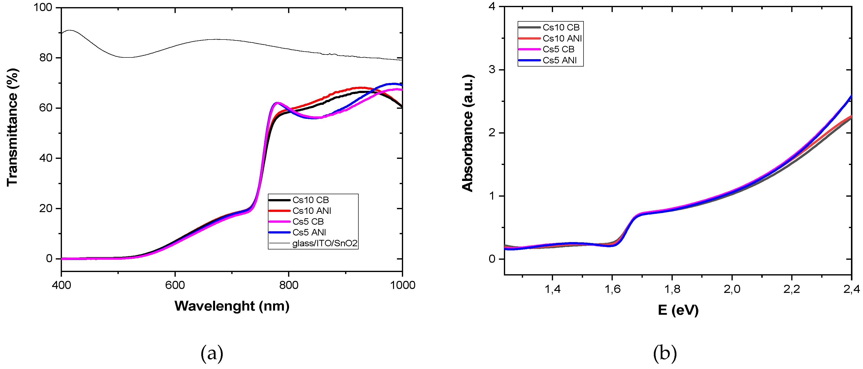
where α is the absorption coefficient of the material, the quantity hν is the energy of light, and m is 2 for a direct bandgap semiconductor. Transmittance was recorded on sample glass/ITO/SnO
2/perovskite. From calculations, the transmittance (T) and absorbance, A, where A=2-log(T), sketched in
Figure 1 (a and b, respectively), have been used for Tauc plot of
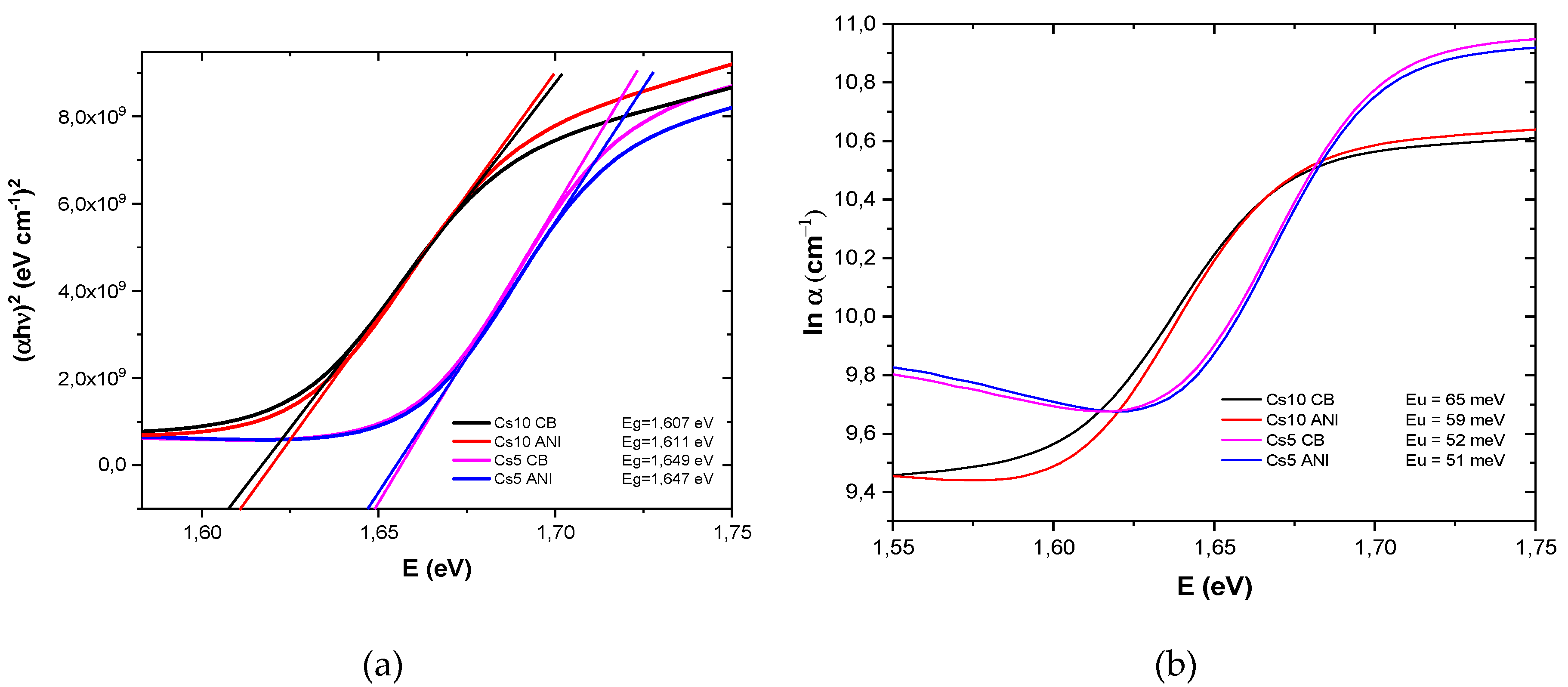
Figure 2a, where α is 2,303 A/d, with d the thickness of perovskite layer, and energy gap is the x intercept.
Urbach energy (E
u) is below the bandgap energy governed by the structural disorder, imperfection and passivation at the surface [
21,
22]. Any modification or deviation from the ideal structure results curvature in the band shape. Thus, the analysis of the optical absorption in the spectral range, corresponding to the tails of the density of states, allows to determine the Urbach energy and thereby characterize the degree of material imperfection. The Urbach energy can be derived using the relation α = α
0 exp(E/E
u), where α is the absorption coefficient, E(=hν) is the photon energy, and E
u is the Urbach energy. The Urbach energy is calculated by plotting ln α vs E. The reciprocal of the slopes of the linear portion, close to energy gap, gives the value of E
u for all the samples (
Figure 2b).
In
Table 2, bandgap and Urbach energies, E
g and E
u, respectively, are reported for all the samples. Energy gap depends on cesium concentration: more cesium means smaller bandgap. Additionally, devices with more cesium exhibit a higher defect density as it is evident from larger Urbach energy. Moreover, when anisole was used as antisolvent, E
u decreased both for Cs10 and Cs5, with indicating less disordered PAL with fewer defects.
3.2. SEM and FIB analyses
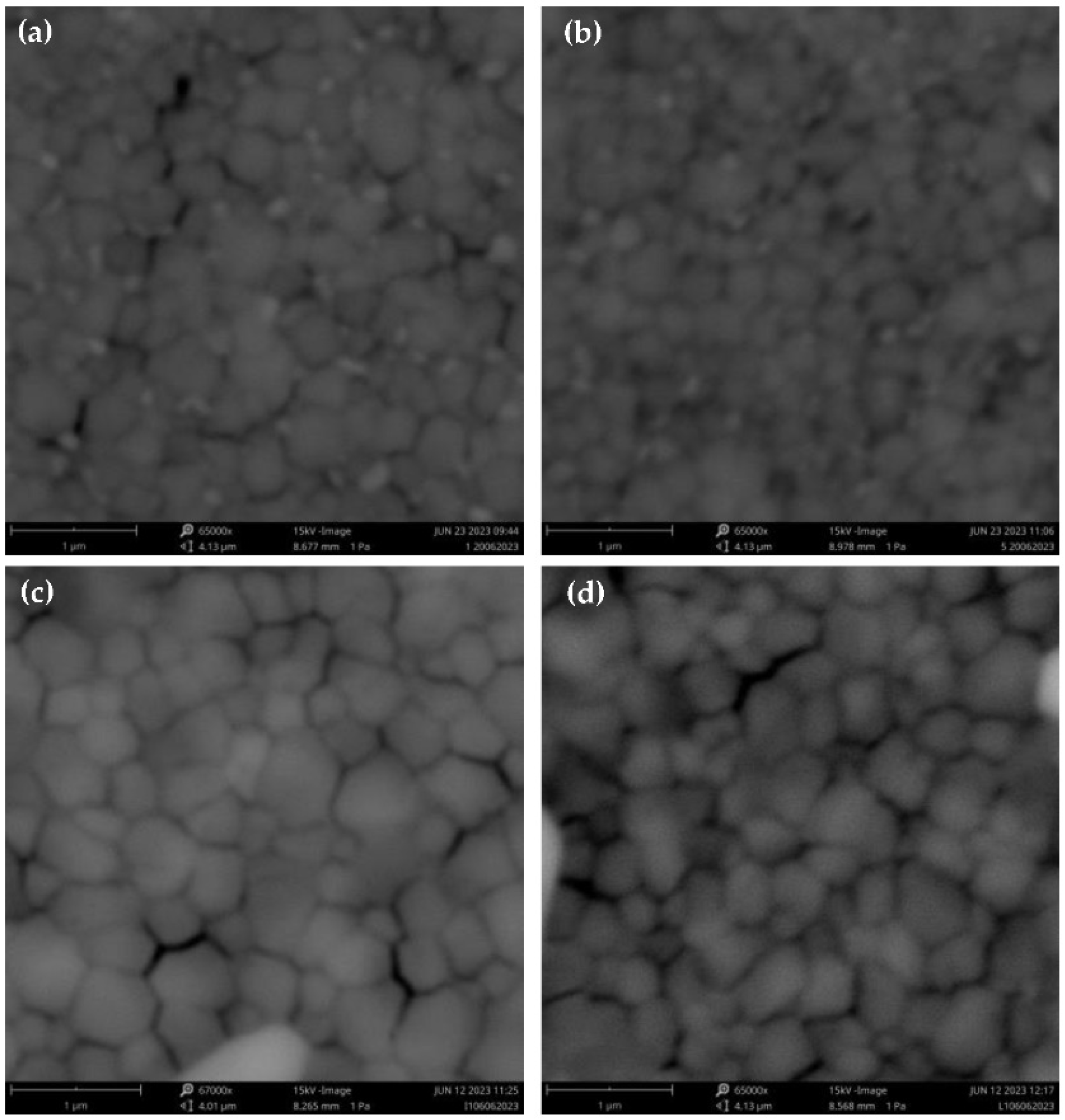
In
Figure 3 we investigated the surface morphologies of PSCs with different cesium composition and antisolvent. It is clear of grain size depends on the concentration of Cesium: higher was the concentration, grains were larger (Fig 3a and 3c). Moreover, there are bright small grains with 5% of Cesium which are attributed to an individual PbI
2 phase [
19], while at 10% of Cs bright grains are not visible. Additionally, there is only little morphology dependence if CB or ANI were used for the same cesium concentration: ANI produces smaller grain size (
Figure 3b and 3d). In
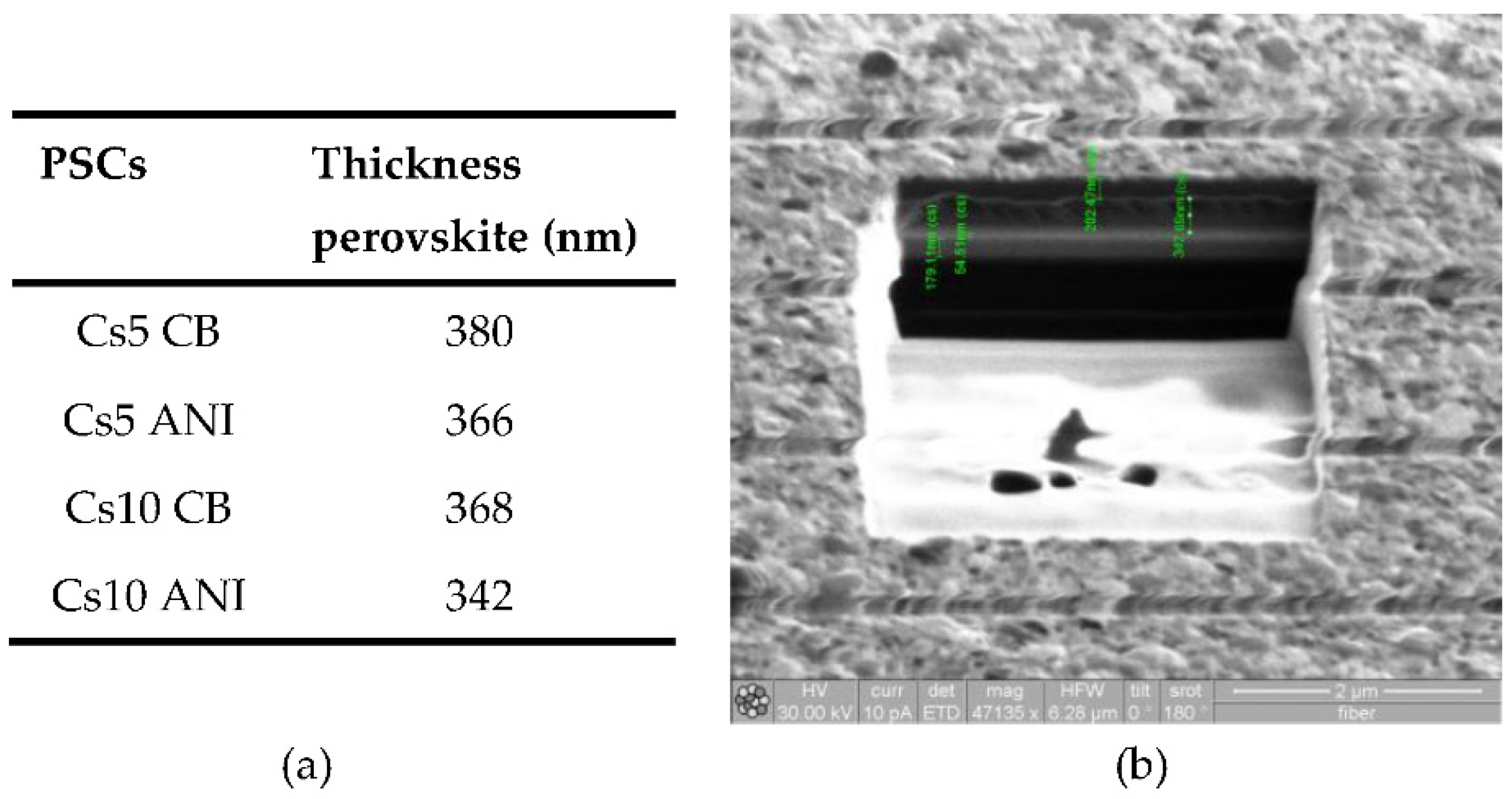
Figure 4 thickness of different devices (
Figure 4a) and a typical cross section (
Figure 4b) were reported.
3.3. J-V characterization
Our unencapsulated perovskite-based devices, entirely fabricated in a glove box (O
2 ≤1ppm and RH ≤1ppm), once the processing was finished, were characterized in an uncontrolled environment, where JV apparatus were located. In
Table 3 temperature and RH range, corresponding to months from April to September, are reported. We observed a strong dependence of electrical performance on humidity and temperature conditions. In fact, best devices were realized and characterized in July when relative humidity was lower.This dependence from relative humidity relating to summer or winter months was also clearly stated by Li et al. [
23].
To ensure the possibility to achieve well-functioning unencapsulated devices, at any time of the year, with changed temperature and relative humidity, several batches with different cesium concentration were realized. It is well known that adding cesium as a third cation makes the triple cation perovskite composition thermally more stable as far as it has less phase impurities and is less sensitive to processing conditions [
17] and less affected by fluctuating surrounding variables such as temperature, humidity, solvent vapours or heating protocols. In fact, we found that, in presence of humidity, higher cesium concentration means higher efficiency. In
Table 4 champion devices are shown and it is also reported our champion devices, with 5% of Cs, realized during winter months when relative humidity was around 30%. It is noticeable that best batches of present work were obtained with 10% of cesium, when RH is higher, while previously, a lower concentration ensured higher efficiency [
18]. In
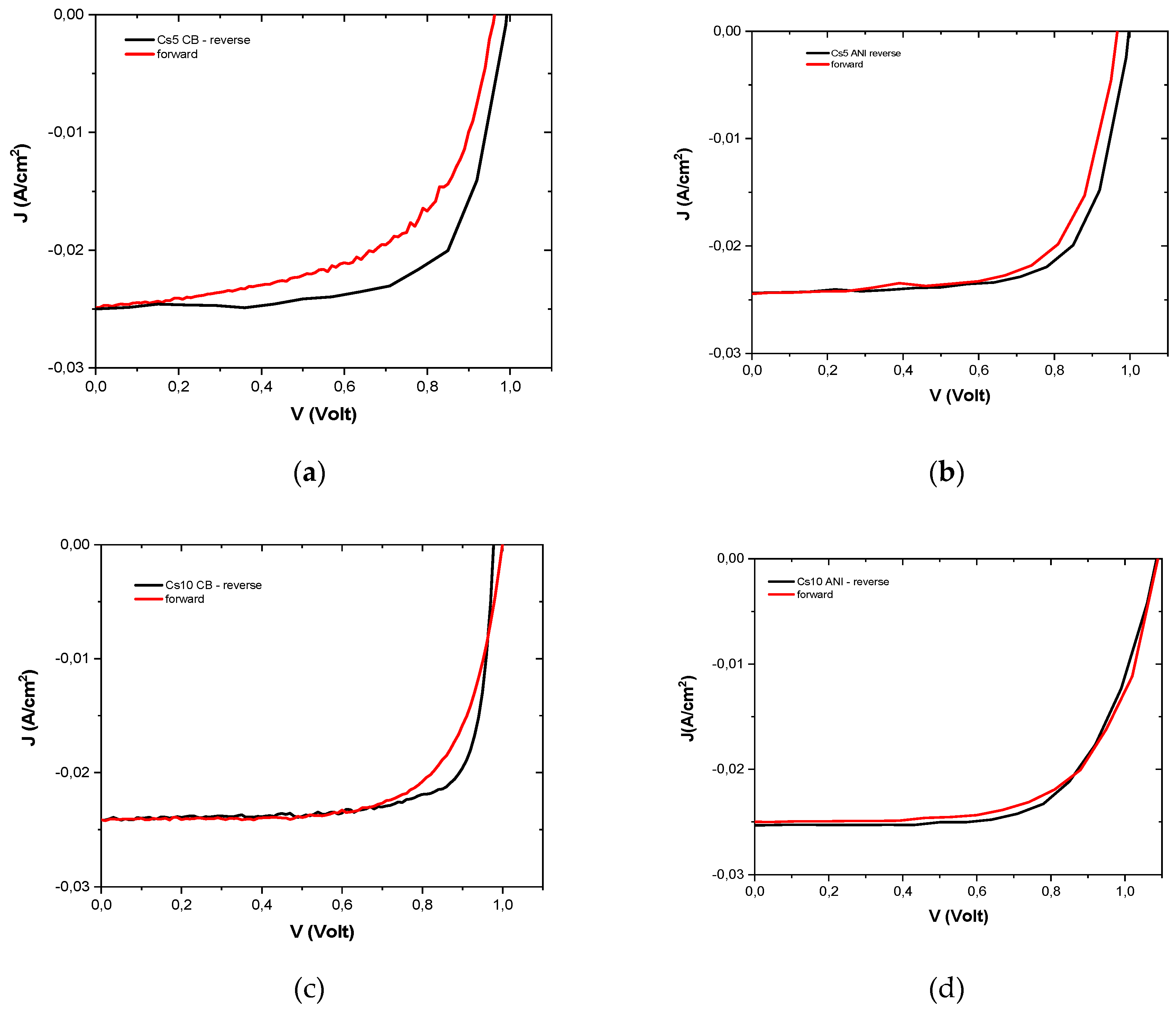
Figure 5 typical JV curves, reverse and forward, are reported and their efficiency, in both scans, was used to calculate the hysteresis index (equation (2)), which is lower for devices with higher Cs concentrations and when ANI was used as antisolvent (
Table 5) [
24].
Typical devices of each type were monitored over 90 days (
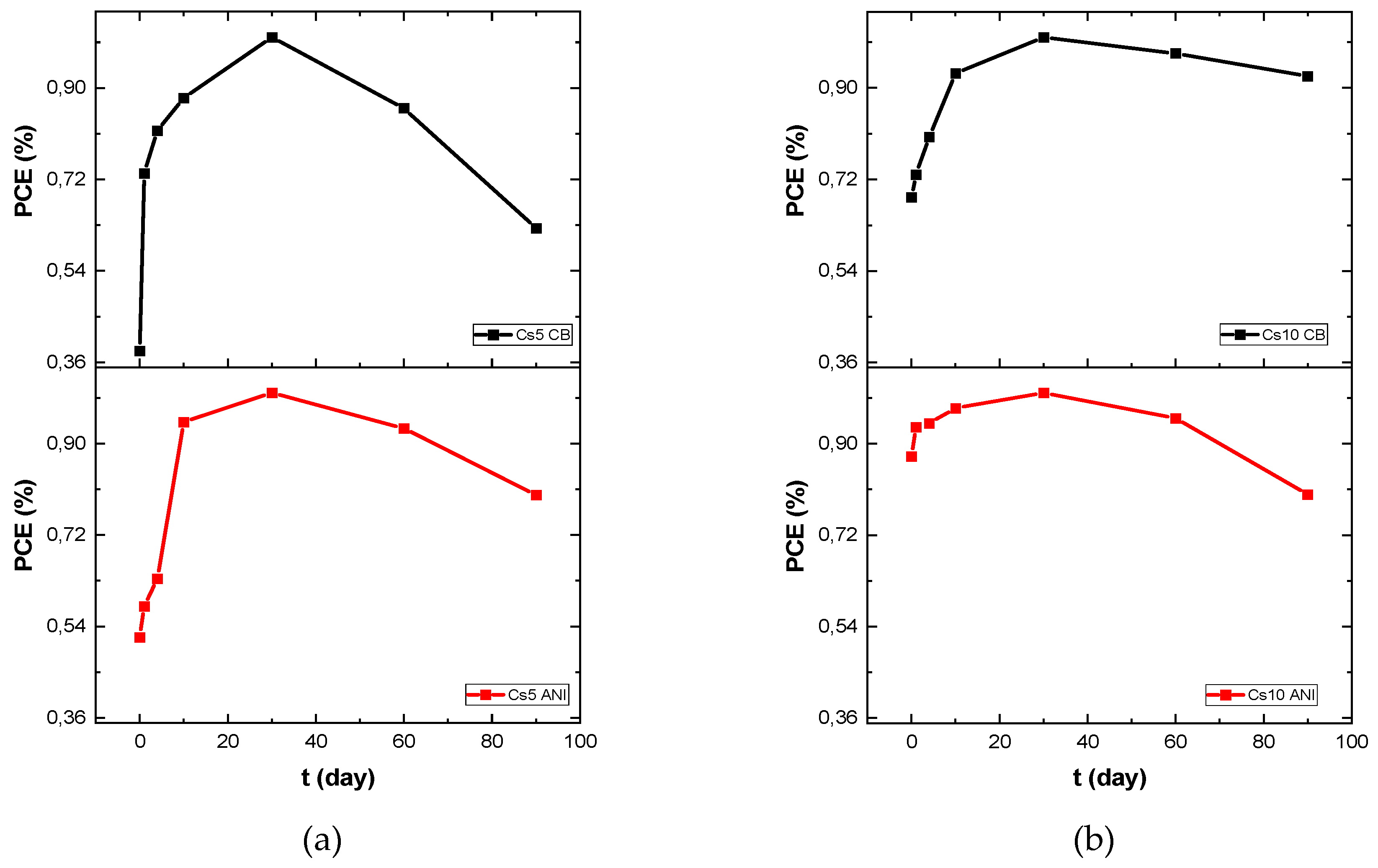
Figure 6) with finding that initial PCE value, at zero time, was very small compared to the maximum for Cs5 CB and Cs5 ANI, while the PCE was very close to the maximum value already in the first measurement when cesium concentration increased. In
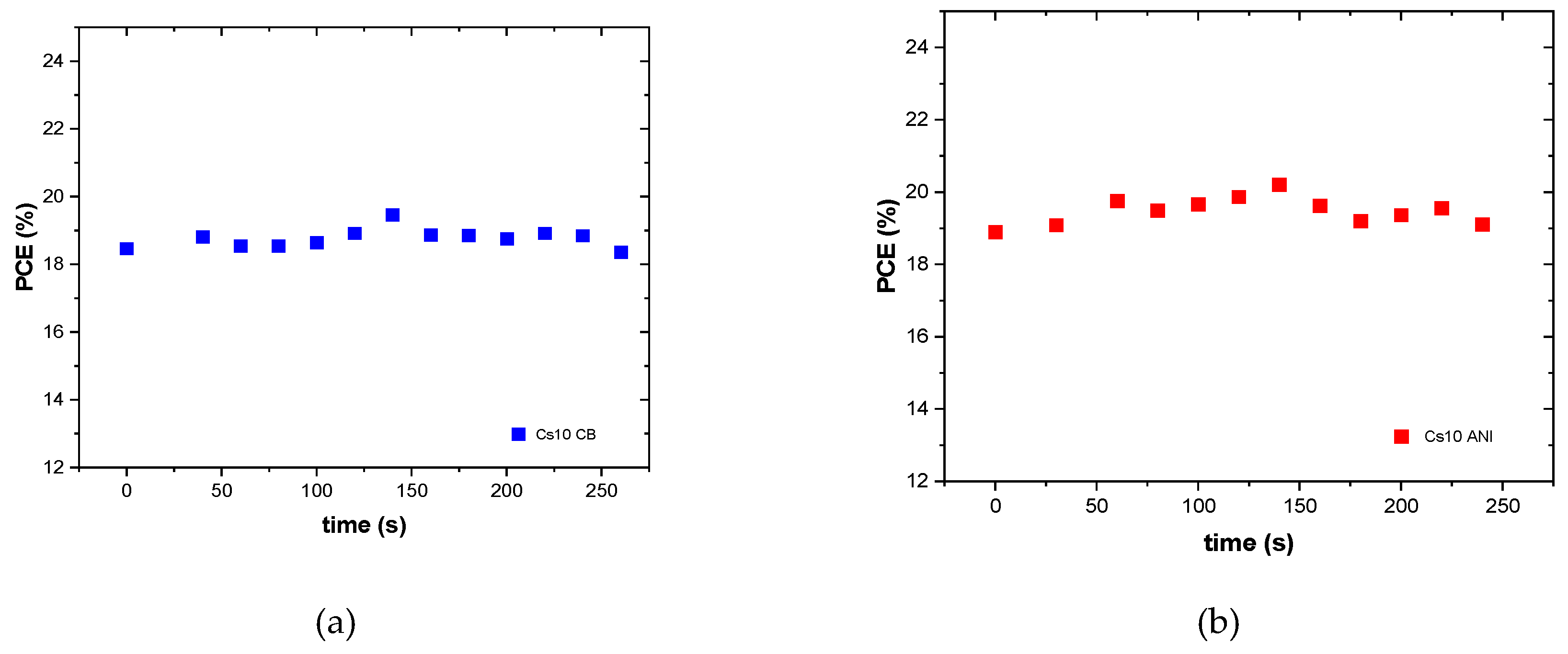
Table 4 PCE, hysteresis index and relative PCE percentage of initial efficiency over 90 days were reported. It is worth noting that devices with anisole maintain 80 percent of their initial efficiency for each cesium concentration. Moreover, they exhibit higher efficiency compared to cells with chlorobenzene. However, it should be emphasized that under extreme conditions of temperature and humidity, devices with a higher concentration of cesium retain much more of their efficiency. Noting that under these environmental conditions, interesting results were obtained for the Cs10 batches, we monitored these devices under continuous illumination (
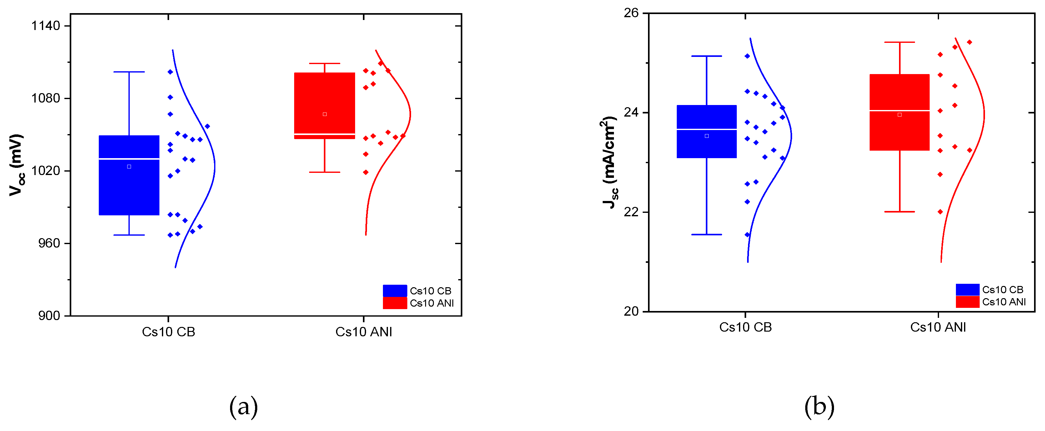
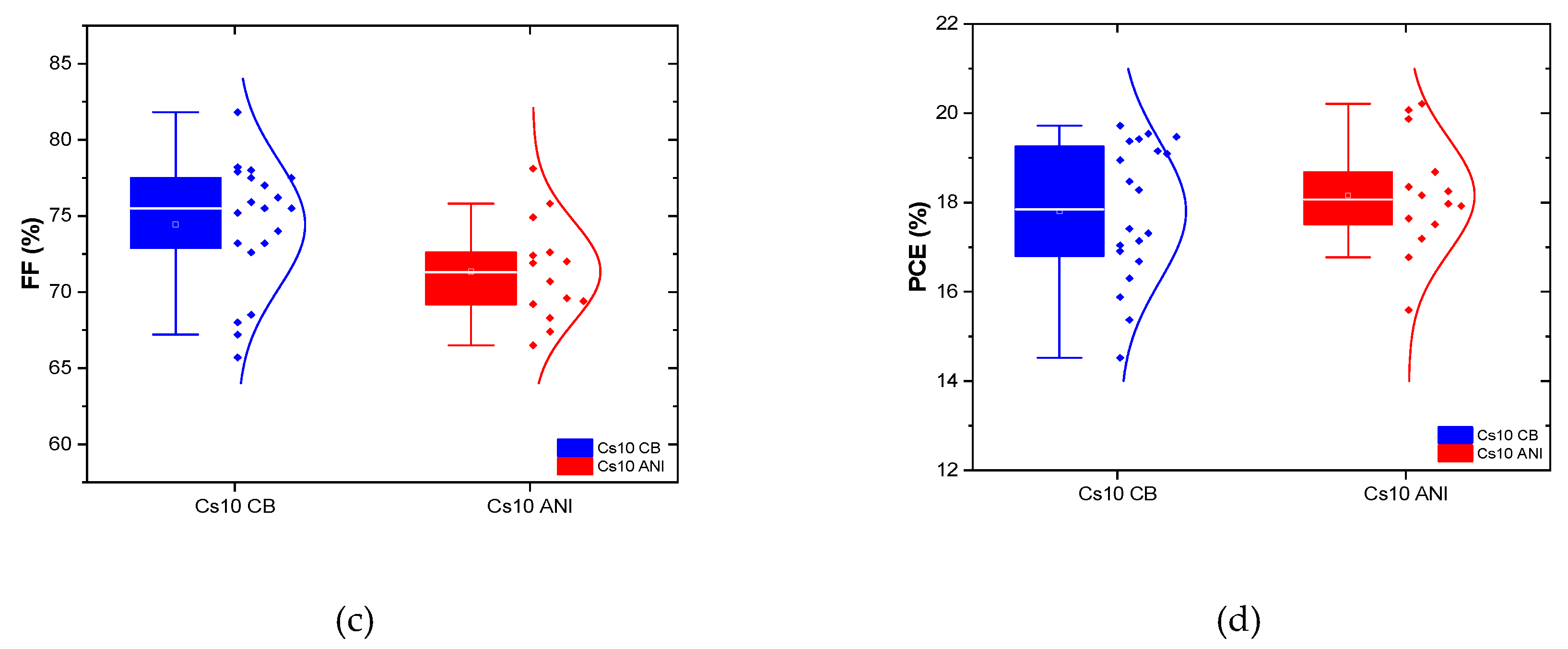
Figure 7) and several batches were realized depicting their performances in the statistical graph shown in
Figure 8. Except the fill factor, which had to be optimized, all the parameters of Cs10 ANI are better than the other batches Cs10 CB.
3.4. Ideality factor
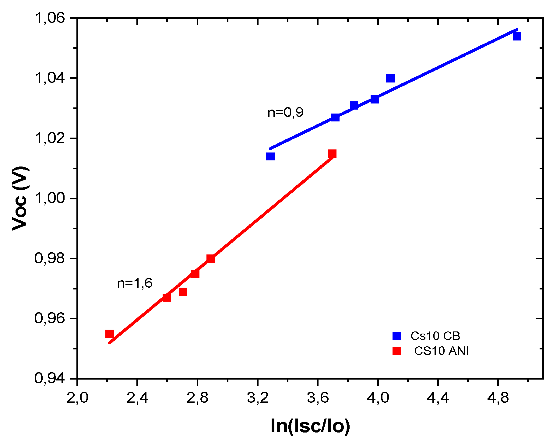
Information about the mode of recombination can be gained by estimating the ideality factor (n) of the solar cell, where an ideality factor close to 1 implies that all the recombination is bimolecular and an ideality factor close to 2 implies that it is monomolecular and is proceeding via trap-assisted recombination [
25]. Under different light exposure, ions will migrate to different regions of solar cells and either make the conditions favorable to stabilize filled traps near the surface of the perovskite absorber layer or make the conditions favorable to induce rapid depopulation of traps. When the traps are mostly filled we expect to have a smaller fraction of trap-assisted recombination, longer charge diffusion lengths and ideality factor closer to 1. When the traps are predominantly empty we expect to have a higher fraction of trap assisted recombination shorter diffusion length and a higher ideality factor. In the field of dye solar cells non integer ideality factors have been explained by the existence of a broad distribution of trap states combined with trap limited recombination [
23]. Then for Cs10ANI ideality factor indicates the both bimolecular and trap assisted recombination are present, while for Cs10 CB only bimolecular recombination is evident [
24]. According also our previous considerations the smaller ideality factor is attributed to the band-band direct recombination confirmed from the higher value of Voc. A lower ion migration makes the devices, Cs10 CB, more stable over time; indeed, after 90 days, the efficiency is approximately 90% of the initial value. At the time, even devices, Cs10 ANI, despite having a higher ideality factor, still maintain about 80% of the initial efficiency.
Ultimately, devices were fabricated from April to July and characterized until September, detecting different temperature and relative humidity range. These conditions are relevant when PSCs are unencapsulated and characterized in air environment [
18,
23]. In fact, our best PSCs were always obtained during dry and with very low external relative humidity days, both in the present work and in previous one [
18]. During summer period, it was more difficult to obtain well-functioning devices using our standard perovskite solution [
18], but increasing the cesium concentration we found that PSCs were more stable although temperature and relative humidity were increased. Moreover, we have stated that anisole can be used as antisolvent because it is able to ensure a good growth of the perovskite film and it is a good sustainable alternative to chlorobenzene.To our knowledge, there are no scientific studies on the use of anisole as an antisolvent for triple-cation perovskite deposited on planar substrates with tin dioxide as the ETL. Anisole was used for triple cation perovskite deposited onto compact or mesoporous TiO
2 (
Table 6). We show then the feasibility of anisole as antisolvent also for the architecture reported in this paper.
5. Conclusions
We explored the potential substitution of the toxic CB with the safer alternative, anisole, in the fabrication of planar triple-cation perovskite solar cells. Anisole proved effective in achieving functional PSCs comparable to those obtained with CB. Notably, devices with anisole as an antisolvent exhibited even lower hysteresis, maintaining 80% of the initial PCE value. These findings reinforce that environmentally friendly anisole can reliably replace the toxic CB. We also varied the cesium concentration in the triple-cation precursor, known for enhancing thermal stability. Higher Cs concentration yielded more stable PSCs, less susceptible to fluctuating temperature and humidity.
Author Contributions
Conceptualization and methodology, V.L.F, A.D.M, G.R; sample fabrication V.L.F, A.D.M, G.R; experimental investigation, V.L.F, A.D.M, G.R, formal analysis, V.L.F; writing—original draft preparation, V.L.F..; writing—review and editing, V.L.F, A.D.M, G.R. All authors have read and agreed to the published version of the manuscript.
Funding
This work was supported by the Italian Ministry of Economic Development in the framework of the Operating Agreement with ENEA for Research on the Electric System.
Data Availability Statement
No new data were created or analyzed in this study. Data sharing is not applicable to this article.
Conflicts of Interest
The authors declare no conflict of interest.
References
- Jeon, N.J.; Noh, J.H.; Kim, Y.C.; Yang, W.S.; Ryu, S.; Seok, S. Solvent engineering for high-performance inorganic–organic hybrid perovskite solar cells. Nat. Mater 2014, 13, 897–903. [Google Scholar] [CrossRef] [PubMed]
- Wang, L.; Wang, x.; Deng, L.; Leng, S.; Guo, X.; Tan, C.; Choy, W.C.H.; Chen, C. The mechanism of universal green antisolvents for intermediate phase controlled high-efficiency formamidinium-based perovskite solar cells. Mater. Horiz., 2020, 7, 934–942. [Google Scholar] [CrossRef]
- Gedamu, D.; Asuo, I.M.; Benetti, D.; Basti, M.; Ka, I.; Cloutie, S. G.; Rosei, F.; Nechache, R. Solvent-Antisolvent Ambient Processed Large Grain Size Perovskite Thin Films for High-Performance Solar Cells. Sci. Rep. 2018, 8, 12885 (1-11). [CrossRef]
- Kwon, N.; Lee, J.; Ko, M.J.; Kim, Y.Y.; Seo, J. Recent progress of eco-friendly manufacturing process of efficient perovskite solar cells. Nano Convergence. 2023, 10–28. [Google Scholar] [CrossRef] [PubMed]
- Tian, S.; Li, J.; Li, S.; Bu, T.; Mo, Y.; Wang, S.; Li, W.; Huang, F. A facile green solvent engineering for up-scaling perovskite solar cell modules. Solar Energy, 2019, 183, 386-391. [CrossRef]
- Zhang, W.; Li, Y.; Liu, X.; Tang, D.; Li, X.; Yuan, X. Ethyl acetate green antisolvent process for high-performance planar low-temperature SnO2-based perovskite solar cells made in ambient air. Chemical Engineering Journal. 2020; 379, 122298. [Google Scholar] [CrossRef]
- Taylor, A.D.; Sun, Q.; Goetz, K.P.; An, Q.; Scheramm, T.; Hofstetter, Y.; Littersrt, M.; Paulus, F.; Vaynzof, Y. . A general approach to high-efficiency perovskite solar cells by any antisolvent. Nat Commun 2021 12, 1878. [CrossRef]
- Crabtree, R.H. . Hypervalency, secondary bonding and hydrogen bonding: siblings under the skin. Chem. Soc. Rev., 2017, 46, 1720. [CrossRef]
- Numata, Y.; Sanehira, Y.; Miyasaka, T. . Drastic Change of Surface Morphology of Cesium–Formamidinium Perovskite Solar Cells by Antisolvent Processing. ACS Appl. Energy Mater, 2021, 4, 2, 1069-1077. [CrossRef]
- Zhao, P.; Kim, B.J.; Ren, X.; Lee, D.G.; Bang, G.J.; Jeon, J.B.; Kim, W.B.; Jung, H.S. Antisolvent with an Ultrawide Processing Window for the One-Step Fabrication of Efficient and Large-Area Perovskite Solar Cells. Adv. Mater. 2018, 30, 1802763. [Google Scholar] [CrossRef] [PubMed]
- Yavari, M.; Mazloum-Ardakani, M.; Gholipour, S.; Tavakoli, M.M.; Turren-Cruz, S-H. ; Taghavinia, N.; Grätzel, M.; Hagfeldt, A.; Saliba M.. Greener, Nonhalogenated Solvent Systems for Highly Efficient Perovskite Solar Cells. Adv. Energy Mater. 2018, 8, 1800177. [Google Scholar] [CrossRef]
- Wang, L.; Wang, X.; Deng, L-L. ; Leng, S.; Guo, X.; Tan, C-H.; Choy, W.C.H.; Chen, C-C.. The mechanism of universal green antisolvents for intermediate phase controlled high-efficiency formamidinium-based perovskite solar cells. Mater. Horiz., 2020, 7, 934–942. [Google Scholar] [CrossRef]
- Habisreutinger, S. N.; Wenger, B.; Snaith, H. J.; Nicholas, R. Dopant-free planar n-i-p perovskite solar cells with steady-state efficiencies exceeding 18%. ACS Energy Lett. 2017, 2, 622–628. [Google Scholar] [CrossRef]
- Zhang, M.; Wang, Z.; Zhou, B.; Jia, X.; Ma, Q.; Yuan, N.; Zheng, X.; Ding, J.; Zhang, W.-H. . Green Anti-Solvent Processed Planar Perovskite Solar Cells with Efficiency Beyond 19%. Sol. RRL, 2018, 2, 1700213. [CrossRef]
- Pellaroque, A.; Noel, N.K.; Habisreutinger, S.N.; Zhang, Y.; Barlow, S.; Marder, S.R.; Snaith, H.J. Efficient and Stable Perovskite Solar Cells Using Molybdenum tris(dithiolene)s as p-Dopants for Spiro-OMeTAD. ACS Energy Lett. 2017, 2, 2044–2050. [Google Scholar] [CrossRef]
- Podapangi, S.K.; Mancini, L.; Xiu, J.; Reddy, S.H.; Di Carlo, A.; Brown, T.M.; Zanotti, G. Green Anisole Solvent-Based Synthesis and Deposition of Phthalocyanine Dopant-Free Hole-Transport Materials for Perovskite Solar Cells. Energies 2023, 16, 3643. [Google Scholar] [CrossRef]
- 17. Saliba, M., Matsui, T.; Seo, J.Y. Domanski, K.; Correa-Baena, J.P.; Nazeeruddin, M.K.; Zakeeruddin, S.M.; Tress, W.; Abate, A.; Hagfeldtd, A.; Grätzela. M. Cesium-containing triple cation perovskite solar cells: improved stability, reproducibility and high efficiency. Energy Environ. Sci., 2016, 9, 1989-1997. [CrossRef]
- La Ferrara, V. , De Maria, A.; Rametta, G.; Delli Veneri, P. The effect of storage cycle on improvement in the photovoltaic parameters of planar triple cation perovskite solar cells. Mater. Adv., 2021, 2, 5396–5405. [Google Scholar] [CrossRef]
- Asmontas, S. , Cerskus, A., Gradauskas, J., Griguceviciene, A.,˙, Leinartas, K., Lucun, A., Petrauskas, K., Selskis, A., Suzied, A., Širmulis, E., Juskenas, R.,, Cesium-Containing Triple Cation Perovskite Solar Cells, Coatings 2021, 11, 279. [CrossRef]
- Im, J-H.; Jang, I-H.; Pellet, N.; Grätzel, M.; Park, N-J. Growth of CH3NH3PbI3 cuboids with controlled size for high-efficiency perovskite solar cells. Nature Nanotechnology, 2014, 9, 927-932. [CrossRef]
- Kiechartz, T.; Pieters, B. E.; Kirkpatrick, J.; Rau, U.; Nelson, J. Recombination via tail states in polythiophene: fullerene solar cells. Phys. Rev. 2011, 83, 115209-22 . [CrossRef]
- Subedi, B.; Li, C.; Chen, C.; Liu, D.; Junda, M.M.; Song, Z.; Yan, Y.; Podraza, N.J. . Urbach Energy and Open-Circuit Voltage Deficit for Mixed Anion-Cation Perovskite Solar Cells. ACS Appl Mater Interfaces 2022, 14, 7796-7804. [CrossRef]
- Li, N.; Niu, X.; Li, L. , Wang, H. , Huang, Z.; Zhang, Y.; Chen, Y.; Zhang, X.; Zhu, C.; Zai, H.; Bai, Y.; Ma, S.; Liu, H.; Liu, X.; Guo, Z.; Liu, G., Fan, R.; Chen, H.; Wang, J.; Lun, Y.; Wang, X.; Hong, J.; Xie, H.; Jacob, D. S.; Hu, X. G.; Chen, Q.; Zhou, H. Liquid medium annealing for fabricating durable perovskite solar cells with improved reproducibility, Science, 2021, 373, 561–567. [Google Scholar] [CrossRef]
- Habisreutinger, S.N.; Noel, N.K.; Snaith, H.J. . Hysteresis Index: A Figure without Merit for Quantifying Hysteresis in Perovskite Solar Cells. ACS Energy Lett. 2018, 3, 10, 2472-2476. [CrossRef]
- Lee, G.W. ; Shim, J-I.; Shin, D-S.. On the ideality factor of the radiative recombination current in semiconductor light-emitting diodes. Appl. Phys. Lett. 2016, 109, 031104. [CrossRef]
- Courtier, N.E. . Interpreting Ideality Factors for Planar Perovskite Solar Cells: Ectypal Diode Theory for Steady-State Operation. Physical review applied,, 2020, 14, 024031. [CrossRef]
- Caprioglio, P.; Wolff, C. M.; Sandberg, O. J.; Armin, A.; Rech, B.; Albrecht, S.; Neher, D.; Stolterfoht, M. ; On the Origin of the Ideality Factor in Perovskite Solar Cells. Adv. Energy Mater. 2020, 10, 2000502. [Google Scholar] [CrossRef]
Figure 1.
(a) Transmittance and (b) absorbance of glass/ITO/SnO2 w/o PAL at different antisolvents and cesium concentration.
Figure 1.
(a) Transmittance and (b) absorbance of glass/ITO/SnO2 w/o PAL at different antisolvents and cesium concentration.
Figure 2.
(a) Tauc plot and (b) Urban energy of glass/ITO/SnO2/perovskite at different antisolvents and cesium concentration.
Figure 2.
(a) Tauc plot and (b) Urban energy of glass/ITO/SnO2/perovskite at different antisolvents and cesium concentration.
Figure 3.
SEM of (a) Cs5 CB; (b) Cs5 ANI (c) Cs10 CB (d) CS10 ANI.
Figure 3.
SEM of (a) Cs5 CB; (b) Cs5 ANI (c) Cs10 CB (d) CS10 ANI.
Figure 4.
(a) in the table reporting thickness PAL acquired by FIB; (b) Typical FIB cross section of Cs10 ANI which also shows different layers of PSCs: ITO, about 180 nm, SnO2, about 54 nm, Cs10 PAL, about 342 nm and Spiro, about 200 nm.
Figure 4.
(a) in the table reporting thickness PAL acquired by FIB; (b) Typical FIB cross section of Cs10 ANI which also shows different layers of PSCs: ITO, about 180 nm, SnO2, about 54 nm, Cs10 PAL, about 342 nm and Spiro, about 200 nm.
Figure 5.
(a) in the table reporting thickness PAL acquired by FIB; (b) Typical FIB cross section of Cs10 ANI which also shows different layers of PSCs: ITO, about 180 nm, SnO2, about 54 nm, Cs10 PAL, about 342 nm and Spiro, about 200 nm.
Figure 5.
(a) in the table reporting thickness PAL acquired by FIB; (b) Typical FIB cross section of Cs10 ANI which also shows different layers of PSCs: ITO, about 180 nm, SnO2, about 54 nm, Cs10 PAL, about 342 nm and Spiro, about 200 nm.
Figure 6.
PCE monitored over 90 days (a) Cs5 CB and ANI; and (b) Cs10 CB and ANI.
Figure 6.
PCE monitored over 90 days (a) Cs5 CB and ANI; and (b) Cs10 CB and ANI.
Figure 7.
PCE measured during continuous illumination for typical devices Cs10 with CB and ANI.
Figure 7.
PCE measured during continuous illumination for typical devices Cs10 with CB and ANI.
Figure 8.
Statistical electrical performance of devices Cs5 and Cs10 with CB and ANI as antisolvents.
Figure 8.
Statistical electrical performance of devices Cs5 and Cs10 with CB and ANI as antisolvents.
Figure 9.
Ideality factor Cs10 CB and Cs10 ANI.
Figure 9.
Ideality factor Cs10 CB and Cs10 ANI.
Table 1.
Properties of main antisolvents used for fabrication process of PSCs.
Table 1.
Properties of main antisolvents used for fabrication process of PSCs.
| Antisolvent |
Molecular Weight (g/mol) |
Boiling Point
(°C) |
Viscosity (cP) |
Solubility in H20 (g/100g) |
Relative polarity |
ICH
Class |
| 1-Butanol |
74 |
118 |
3.006 |
7.7 |
0.586 |
3 |
| Ethyl Acetate |
88 |
77 |
0.443 |
8.7 |
0.228 |
3 |
| Anisole |
108 |
154 |
0.789 |
0.10 |
0.198 |
3 |
| Chlorobenzene |
113 |
131 |
0.760 |
0.05 |
0.188 |
2 |
Table 2.
Bandgap and Urbach energies for all the samples at different cesium concentration and antisolvent.
Table 2.
Bandgap and Urbach energies for all the samples at different cesium concentration and antisolvent.
| Glass/ITO/SnO2/perovskite |
Eg (eV) |
Eu (eV) |
| Cs10 CB |
1.607 |
0.065 |
| Cs 10 ANI |
1.611 |
0.059 |
| Cs5 CB |
1.649 |
0.052 |
| Cs5 ANI |
1.647 |
0.051 |
Table 3.
Temperature and Relative humidity range from April to September.
Table 3.
Temperature and Relative humidity range from April to September.
| Months |
Temperature range (°C) |
Relative Humidity (%) |
April
May |
10-17
17-28 |
55-85
62-93 |
| June |
24-31 |
52-87 |
| July |
29-37 |
45-73 |
| September |
26-37 |
41-76 |
Table 4.
JV parameters of champion devices of present work and previous champion device [
18].
Table 4.
JV parameters of champion devices of present work and previous champion device [
18].
| Device |
JV parameters |
| Cs5 CB |
Voc = 1005 mV |
| Jsc = 26.04 mA/cm2
|
| FF = 70.9 % |
| PCE = 18.58 % |
Cs5 CB
our previous work [18] |
Voc = 1121 mV
Jsc = 24.07 mA/cm2
FF = 77.3 %
PCE = 20.9 % |
| Cs5 ANI |
Voc = 1006 mV |
| Jsc = 25.54 mA/cm2
|
| FF = 72.3 % |
| PCE = 18.58 % |
| Cs10 CB |
Voc = 984 V |
| Jsc = 23.79 mA/cm2
|
| FF = 81.8 % |
| PCE = 19.15 % |
| Cs10 ANI |
Voc = 1049 mV |
| Jsc = 25.42 mA/cm2
|
| FF = 75.8 % |
| PCE = 20.21 % |
Table 5.
Typical electrical performances, extrapolated from data of
Figure 4, hysteresis index and PCE percentage of its initial efficiency over 90 days.
Table 5.
Typical electrical performances, extrapolated from data of
Figure 4, hysteresis index and PCE percentage of its initial efficiency over 90 days.
| Glass/ITO/SnO2/perovskite |
PCE reverse (%) |
PCE forward (%) |
HI |
Relative %PCE over 90 days |
| Cs5 CB |
17.03 |
13.85 |
0.18 |
62 |
| Cs 5 ANI |
17.10 |
16.10 |
0.06 |
80 |
| Cs10 CB |
18.28 |
16.64 |
0.09 |
92 |
| Cs10 ANI |
18.20 |
17.76 |
0.02 |
80 |
Table 6.
Papers where anisole was used as antisolvent.
Table 6.
Papers where anisole was used as antisolvent.
| ARCHITECTURE (glass/TCO) |
JV parameters |
Storage and aging time |
Final relative PCE |
REF |
compactTiO2/mesoTiO2/
Cs0.05(MA0.17FA0.83)(0.95)Pb(I0.83Br0.17)3
|
Voc = 1.15 V |
<20% RH
@ RT – 1000 h |
93% |
[10] |
| Jsc = 21.98 mA/cm2
|
| FF = 78 % |
| PCE = 19.76 % |
| compactTiO2/meso TiO2/ Cs0.05(MA0.17FA0.83)(0.95)Pb(I0.83Br0.17)3 |
Voc = 1.12 V |
MPPT – 60 s |
|
[11] |
| Jsc = 23.26 mA/cm2
|
| FF = 76 % |
| PCE = 19.88 % |
| compactTiO2/meso TiO2/ Cs0.05(MA0.17FA0.83)(0.95)Pb(I0.83Br0.17)3 |
Voc = 1.10 V |
MPPT – 45 s |
|
[12] |
| Jsc = 22.23 mA/cm2
|
| FF = 75 % |
| PCE = 18.43 % |
| compact TiO2/ Cs0.05(MA0.17FA0.83)(0.95)Pb(I0.83Br0.17)3
|
Voc = 1.10 V |
MPPT – 100 s |
|
[13] |
| Jsc = 22.78 mA/cm2
|
| FF = 77 % |
| PCE = 19.42 % |
| SnO2/ FA0.83MA0.117Pb(I0.87Br0.17)3
|
Voc = 1.14 V |
MPPT – 45 s |
|
[14] |
| Jsc = 22.07 mA/cm2
|
| FF = 75 % |
| PCE = 18.9 % |
| SnO2/ FA0.83MA0.117Pb(I0.87Br0.17)3
|
Voc = 1.11 V |
30% humidity
@ 85°C – 500 h |
50% |
[15] |
| Jsc = 21.96 mA/cm2
|
| FF = 73 % |
| PCE = 18.2 % |
SnO2/ Cs0.1(MA0.17FA0.83)(0.9)Pb(I0.83Br0.17)3
|
Voc = 1.05 V
Jsc = 25.42 mA/cm2
FF = 76 %
PCE = 20.2 % |
41-76% RH
@ 26-37 °C-2160 h |
80% |
Present work |
|
Disclaimer/Publisher’s Note: The statements, opinions and data contained in all publications are solely those of the individual author(s) and contributor(s) and not of MDPI and/or the editor(s). MDPI and/or the editor(s) disclaim responsibility for any injury to people or property resulting from any ideas, methods, instructions or products referred to in the content. |
© 2023 by the authors. Licensee MDPI, Basel, Switzerland. This article is an open access article distributed under the terms and conditions of the Creative Commons Attribution (CC BY) license (http://creativecommons.org/licenses/by/4.0/).
