
You are currently viewing a beta version of our website. If you spot anything unusual, kindly let us know.
Preprint
Article
Early Periods of Low-Temperature Linear Antenna Cvd Nucleation and Growth Study of Nanocrystalline Diamond Films
Altmetrics
Downloads
97
Views
25
Comments
0
A peer-reviewed article of this preprint also exists.


This version is not peer-reviewed
Abstract
: Low-temperature growth of diamond films by chemical vapor deposition (CVD) method is not so widely reported and especially its initial periods of nucleation and growth phenomenon are of particular interest to the researchers. Four sets of substrates were selected for growing diamond films by linear antenna microwave plasma enhanced CVD (LA-MPCVD). Among them, silicon and sapphire substrates were pre-treated with detonation nanodiamond (DND) seeds before diamond growth for enhancement of its nucleation. On the other hand, carbon nanotube (CNT) films on Si substrates were also used as another template for LA-MPCVD diamond growth. In order to enhance the diamond nucleation during CVD growth, some of the CNT films were again pre-treated by electrophoretic deposition (EPD) of diamond nanoparticles. All these substrates were then put inside the LA-MPCVD chamber for growing diamond films under variable processing conditions. Microwave input powers (1100 – 2800 W), input power modes (pulse or continuous), antenna to stage distances (5 - 6.5 cm), process gas recipes (with or without CO2), methane gas percentages (3 - 5%), deposition times (11 – 120 minutes) were altered to investigate their effect on the growth of diamond film on the pre-treated substrates. The substrate temperatures were found to vary from as low as 170oC to a maximum of 307oC during the alteration of the different processing parameters. Contrary to the conventional MPCVD, it was observed that during the first hour of LA-MPCVD diamond growth, DND seeds or the nucleating structures, do not coalesce together to make a continuous film. Deposition time was the most critical factor in fully covering the substrate surfaces with diamond film, since the substrate temperature could not become stable during the first hour of LA-MPCVD. CNT was found to be oxidised rapidly under LA-MPCVD plasma conditions; therefore, a CO2-free process gas recipe was used to reduce CNT burning. Moreover, EPD-coated CNT was found to be less oxidised by the LACVD plasma during diamond growth.
Keywords:
Subject: Chemistry and Materials Science - Surfaces, Coatings and Films
1. Introduction
CVD growth of diamond films occurs within the temperature range of 700-1100oC [1]. There are also reports of growing diamond films at substrate temperatures of 500oC or less [2,3,4,5,6]. Linear antenna microwave plasma enhanced CVD (LA-MPCVD) is a process [7,8,9,10,11,12,13] that allows growing diamond crystals at lower substrate temperatures [14,15,16]. However, there is very little literature available where growth has been reported at less than 300oC temperature [17,18]. Reporting of the respective substrate temperature during CVD has mostly been done in situ, by optical pyrometers [19], but low LA-MPCVD processing temperatures do not allow to use of such optical instruments [15]. Therefore, thermocouples and infrared thermometers are placed underneath the substrate stage to record reliably the LA-MPCVD growth temperatures, where it is protected or uninfluenced from the effect of CVD plasma in the diamond growth environment. In this paper, experiments have been designed to allow diamond growth at less than 300oC. It is also well known that during the first few minutes of CVD deposition, diamond film coalesces together to cover the entire pre-seeded substrate surface [20]. Due to the very slow growth rates (5-50 nm/hr) during the LA-MPCVD process, all the above cited articles have been reported to grow continuous nanocrystalline diamond (NCD) films over long (8-20 hrs) deposition periods. But there is little or no information about diamond growth behaviour during the first hour of LA-MPCVD processing. Neither there is any data over the time period which should be allowed to effectively cover the substrate surface under LA-MPCVD processing conditions [21,22]. The primary obstacle in chemically synthesising diamond is the fact that the starting point should be diamond itself as seed particles. Without appropriate nucleating agent, diamond growth incubation time can be very long, and researchers have tried many methods for the nucleation enhancement during CVD growth of diamond [23,24,25,26,27]. Mechanical or ultrasonic scratching of the substrates with abrasives [28,29] and detonation nanodiamond (DND) seeding [30,31] are the most commonly used techniques for promoting nucleation of diamond films before starting the CVD process. However, there are very few reports of nucleation enhancement by electrophoretic deposition (EPD) [32,33,34,35]. Here it has been attempted for the first time, both the EPD and DND seeding techniques for nucleation enhancement on different substrates.
Potocky et al. [36,37] also investigated the growth of carbon nanotubes (CNT) using linear antenna CVD system with RF biasing of the substrate for 10 min and 40 min durations. Another paper from the same research group [18] reported LA-MPCVD plasma treatment of polymer passivated NCD layers for enhancement of the diamond surface conductivity by surface hydrogenation. Their research showed that 200oC is the optimum substrate temperature to effectively hydrogenate the NCD surface and simultaneously without damaging the metallic contacts or the top polymeric resist layer used for electronics. Potocky et al. [36] concluded that CNTs grown by LA-MPCVD are hydrophobic with contact angle greater than 130o. They used oxygen plasma treatment of 5 min. for enhancing the CNT surface wettability. But they did not attempt to grow diamond films on top of their CNTs [38], which has so far been attempted by the researchers with limited success. It has been reported that CNT covered with NCD are better field effect transmitters [39,40]. In the present work, CNT was grown separately by a thermal CVD reactor on Si substrates, before performing LA-MPCVD of the diamond films onto them. But being hydrophobic, CNT could not be seeded (essential for growing diamond by CVD) with water based DND solution, as could be done for other regular hydrophilic silicon or sapphire substrates. Therefore, EPD was used for seeding the CNT/Si substrate with nanodiamonds for further diamond growth by LA-MPCVD. Such diamond coated CNTs will have applications in electron field emission.
2. Materials and methods
2.1. Substrates
Silicon and sapphire substrates, laser cut into 10×10 mm2 sizes, were used for CVD diamond growth. Silicon substrates were cut out from commercially available p-type 0.5 mm thick 4-inch wafers with a resistivity of 20 ohm-cm. Sapphire substrates were single crystal wafers from the commercial supplier Kyocera. Both of them were seeded with nanodiamonds to enhance the diamond nucleation during CVD growth as described in section 2.1.1.
2.1.1. DND seeding
Water-based detonation nanodiamond (DND) slurry was spin-coated on top of the silicon and sapphire substrates with a rotating speed at 4000 rpm by a spin coater (Laurell Technologies Corporation, model WS-400B-6NPP/LITE) for 40 sec, along with brief rinsing with distilled water, until the surfaces become completely dry [41]. Such monolayer-seeded substrates were then loaded into the LA-MPCVD chamber. Figure 1a is the SEM image of the DND-seeded silicon substrate. The nucleation density was calculated to be 2×10¹⁰/cm2. Figure 1b is the x-ray diffraction of the sapphire substrate used in this study.
2.1.2. CNT and EPD
Other than the conventional DND seeding procedure, two separate sets of silicon substrates were also prepared. One set of substrates was carbon nanotubes (CNT) deposited on silicon wafers by iron catalyst-assisted thermal CVD. The other set was prepared by further electrophoretically depositing diamond on top of such CNT/Si substrates.
The growth conditions of CNTs were a working pressure of 3 Torr, a growth time of 20 min at 750℃ with gas flow rates of NH3 and C2H2 of 10 sccm and 40 sccm, respectively. Figure 1c shows the SEM image of the top surface of the CNT/Si substrate. The length of CNTs was found to be 510 µm (inset).
In order to protect the CNTs from plasma damage during deposition of the diamond film, the diamond nanoparticles were coated on top of the CNTs by electrophoretic deposition (EPD). In the EPD process, water based nanodiamond solution (Nanoseed 18 by Micro Diamant AG Switzerland) was used. The earlier prepared CNTs/Si substrates were biased at about +20 V with respect to the reference electrode, the Pt, for 20 s. Figure 1d shows the SEM photograph of the diamond nanoparticles on top of the CNT/Si substrate. The nucleation density was estimated at about 4.7×10¹⁰/cm2.
Figure 1.
(a) SEM image of the DND seeded silicon substrate, (b) XRD of sapphire substrate, (c) CNT coated silicon substrate, inset SEM showing cross-sectional CNT length and (d) top view of the EPD of diamond nanoparticles on the CNT/Si substrate.
Figure 1.
(a) SEM image of the DND seeded silicon substrate, (b) XRD of sapphire substrate, (c) CNT coated silicon substrate, inset SEM showing cross-sectional CNT length and (d) top view of the EPD of diamond nanoparticles on the CNT/Si substrate.

2.2. LA-MPCVD
All the four set of substrates were loaded together inside the linear antenna microwave plasma-enhanced CVD chamber. No heater was used for additional heating of the substrates. Total volume of the process gases was fixed at 150 sccm and therefore, the working pressure was also fixed at 0.23 mbar. The base pressure achieved before starting the deposition run was in the order of 10-4 Torr. The experimental conditions are described in the following Table 1.
Deposition periods were varied from 11-120 minutes. The substrates were solely heated by the microwave plasma, therefore, depending on the individual CVD period, the substrate stage temperatures were different, as described in the Table 1. For example, samples # LA200519-1 were loaded at room temperature of 21oC inside the LA-MPCVD chamber and after achieving the base pressure of 7×10⁻⁴ Torr, the plasma was ignited with the introduction of the processing gases. 1500 W of average power was achieved by switching on two 2.45 GHz magnetrons. The deposition was carried out for 60 minutes and the final temperature recorded was 284oC. It is to be noted that the substrate stage temperature continues to rise during the whole deposition period and the LA-MPCVD plasma heating profiles are depicted in Figure 2. After the each CVD run was over, the plasma was put off by disconnecting power supplies to the magnetrons and only the hydrogen gas was allowed to flow through, in order to cool down the substrate stage below 140 oC (permissible temperature safety limit of the reactor), before unloading and loading the next set of 4-substrates. An example of LA-MPCVD cycle of cooling with hydrogen gas flow, thereafter plasma heating (11-minute-long for samples # LA200605-3) and again successive cooling profile is shown in Figure 2b. However, if the deposition time is long enough like that for the samples # LA200520-2, the temperature profile looks very much stable and flat at 263oC towards the end of the LA-MPCVD run, as shown in Figure 2c. Table 1 describes widely variable heating rates because the non-linear nature of the respective heating profiles by the plasma. During the initial LA-MPCVD periods, the temperature rise was steeper, which thereafter slows down to a flatter curve (Figure 2a), before achieving a flat stable temperature regime (Figure 2c). Figure 2d describes the plasma heating of the four samples together during the LA-MPCVD D run. The processing was either with CO2 or without CO2 gas in the precursor recipe as shown in the Table 1. The reactor chamber was intermittently plasma cleaned by flowing 200 sccm oxygen at 2800 W average input microwave power, for a time duration, matching with the previously concluded CVD run period. The minimum duration of CVD run was 11 minutes, whereas, the maximum CVD time was 2 hr long in the current set of experiments. The distances were 5 and 6.5 cm between the substrate stage and the linear antenna quartz tube, as determined by trial and errors, for optimum NCD film generation. The microwave input power was mostly in continuous wave (CW) mode, except for one set of experiments (samples # LA200525), in which pulsed mode input microwave power was applied at 20 kHz frequency and 45% duty cycle.
2.3. Physical characterisations
The samples were examined by scanning electron microscope (SEM- FEI Quanta 200 FEG) for evaluating the efficacies of different processing conditions of the CVD diamond growth. Raman spectroscopy (HORIBA Jobin Yvon T64000 spectrometer using laser light of 488 nm wavelength) was also used to confirm the presence of nanodiamond film. X-ray diffraction (XRD) was used to get the characteristic substrate peaks for sapphire.
3. Results and discussion
In this work, silicon and sapphire substrates have been seeded following standard DND monolayer dispersion technique [41] before growing diamond by LA-MPCVD [15]. Another set of substrates with CNT on silicon were also prepared for LA-MPCVD diamond growth of diamond. Conventional water based DND suspension could not be used for seeding the CNT/Si substrates since the as-grown CNT was hydrophobic. Therefore, EPD was used to seed the CNT/Si substrate for nucleation enhancement, reported here for the first time, before LA-MPCVD growth. It is expected that EPD treated diamond will be better template for diamond growth than untreated CNT/Si substrate for growing diamond inside the LA-MPCVD reactor.
3.1. First hour of LA-MPCVD growth
3.1.1. Silicon substrates
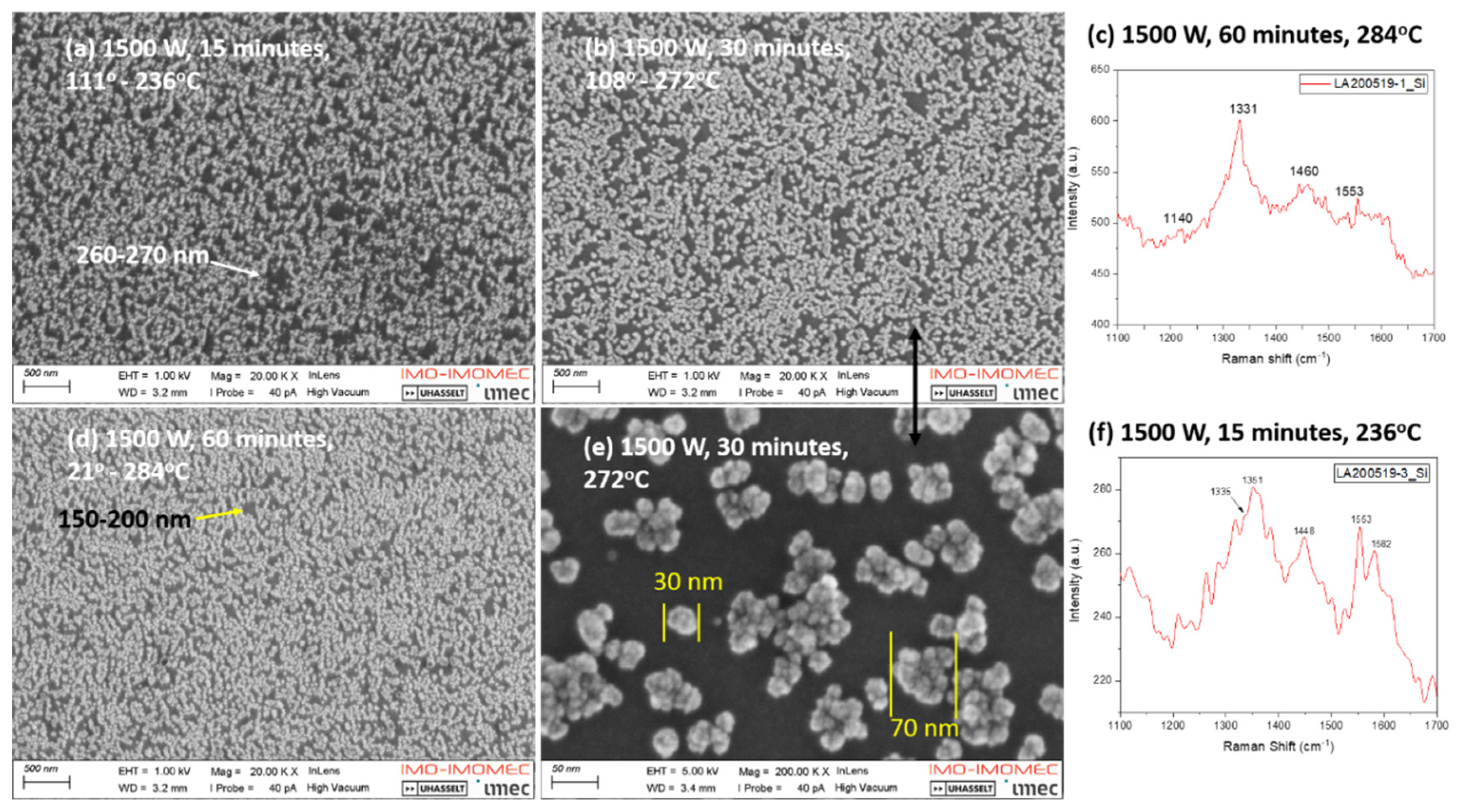
Figure 3 compares the NCD growth patterns after 15, 30 and 60 minutes of LA-MPCVD runs. Figure 3a, Figure 3b and Figure 3d show gradual increase in the size of the diamond nanocrystals with increasing deposition time. After the first 15 minutes of LA-MPCVD, the nanodiamond seed crystals, which are typically 4-6 nm in sizes or their agglomerates (Figure 1a), grew into bigger sizes but did not become large enough to effectively touch each other in order to form connecting network of diamond nanocrystals (Figure 3a – the current SEM image magnification was not high enough to determine the respective NCD sizes after 15 minutes of LA-MPCVD growth). As the deposition time is increased to 30 minutes and further into 60 minutes of LA-MPCVD, the diamond nanocrystals start touching each other but still not enough to completely cover the underlying silicon substrate. The black contrasting substrate features are gradually found to diminish in the corresponding SEM images (Figure 3a, Figure 3b and Figure 3d, respectively). It was easier to calculate the uncovered substrate surface areas than the size of the individual NCDs grown over them after 15 minutes of LA-MPCVD. The average lengths of the uncovered silicon substrate areas were more than 270 nm (Figure 3a) after 15 minutes of LA-MPCVD run, and were reduced but not enough to let the nanodiamond crystals touch each other after 30 minutes of LA-MPCVD, as shown in Figure 3e. The sizes of the nanodiamond seed crystals is found to grow to about 30 nm isolated nanocrystals or to their agglomerates of 60-70 nm sizes in Figure 3e. Even after 60 minutes of LA-MPCVD, 150-200 nm long uncovered silicon areas were still visible in Figure 3d. It is important to notice that the 30 nm or 70 nm NCDs, shown in Figure 3e are actually agglomerations of tinier (about 10 nm) nanoparticles.
The Raman spectra from the diamond nanocrystals after 15 minutes of LA-MPCVD is found to be very noisy (Figure 3f) with a small sp3 peak at 1335 cm-1 in contrast to disordered graphite (D) band at 1351 cm-1. There are also Raman peaks at 1448, 1553 and 1582 cm-1, which correspond to trans-poly-acetylene (TPA) and graphite crystals (G) respectively in the growing NCD film. On the other hand, the sp3 Raman signal after 60 minutes of LA-MPCVD diamond growth is found to be very strong (Isp3= 156) with FWHM of 18 cm-1 (Figure 3c). The corresponding non-diamond Raman peaks for TPA (1140 and 1480 cm-1) and G-band (1553 cm-1 and hump thereafter) are also present but at much-reduced level (Isp2=60), indicating growth of good quality diamond nanocrystals. The sp3 Raman peak signal enhancement in Figure 3c in comparison to Figure 3f is due to the combined effect of increased LA-MPCVD deposition time, which also helped to achieve higher substrate temperatures. It is important to note that the NCD growth temperature is dynamic and continuously increasing by the deposition time over which the stage was allowed to be heated by the microwave plasma. The longer the CVD time period, the higher the substrate temperature - until the substrate temperature becomes gradually stable with the progressing time. 15-60 minutes of heating by the plasma does not allow the substrate temperature to become stabilised (Figure 2a).
Figure 3.
NCD crystals on DND seeded silicon substrates, (a) SEM of the sample grown after first 15 minutes, (b) SEM of the sample grown after 30 minutes at 20kX magnification, (c) Raman spectra of the sample grown after 60 minutes, (d) SEM of the sample grown after 60 minutes, (e) SEM of the sample grown after 30 minutes at 200kX magnification and (f) Raman spectra after of the sample grown 15 minutes of LA-MPCVD growth.
3.1.2. Sapphire substrates
Figure 4 shows the corresponding Raman spectra from the NCDs grown over DND-seeded sapphire substrates, kept alongside the silicon substrates as shown in Figure 2d. Here it is also found that the sp3 Raman peak in and around 1331 cm-1 is the sharpest with a FWHM of 15 cm-1 (Figure 4a), from the NCD grown over the longer time period of 60 minutes. In fact, NCDs grown over sapphire substrate have better FWHM values than NCDs grown over silicon substrates (Figure 3c). The sp3 Raman signals become gradually weaker (figures 4b and 4c) and other non-diamond peaks (TPA - 1491, graphitic D - 1350 and G – 1600 cm-1) become stronger due to the presence of smaller NCDs, with the reduction in LACVD time periods.
3.1.3. CNT and EPD substrates
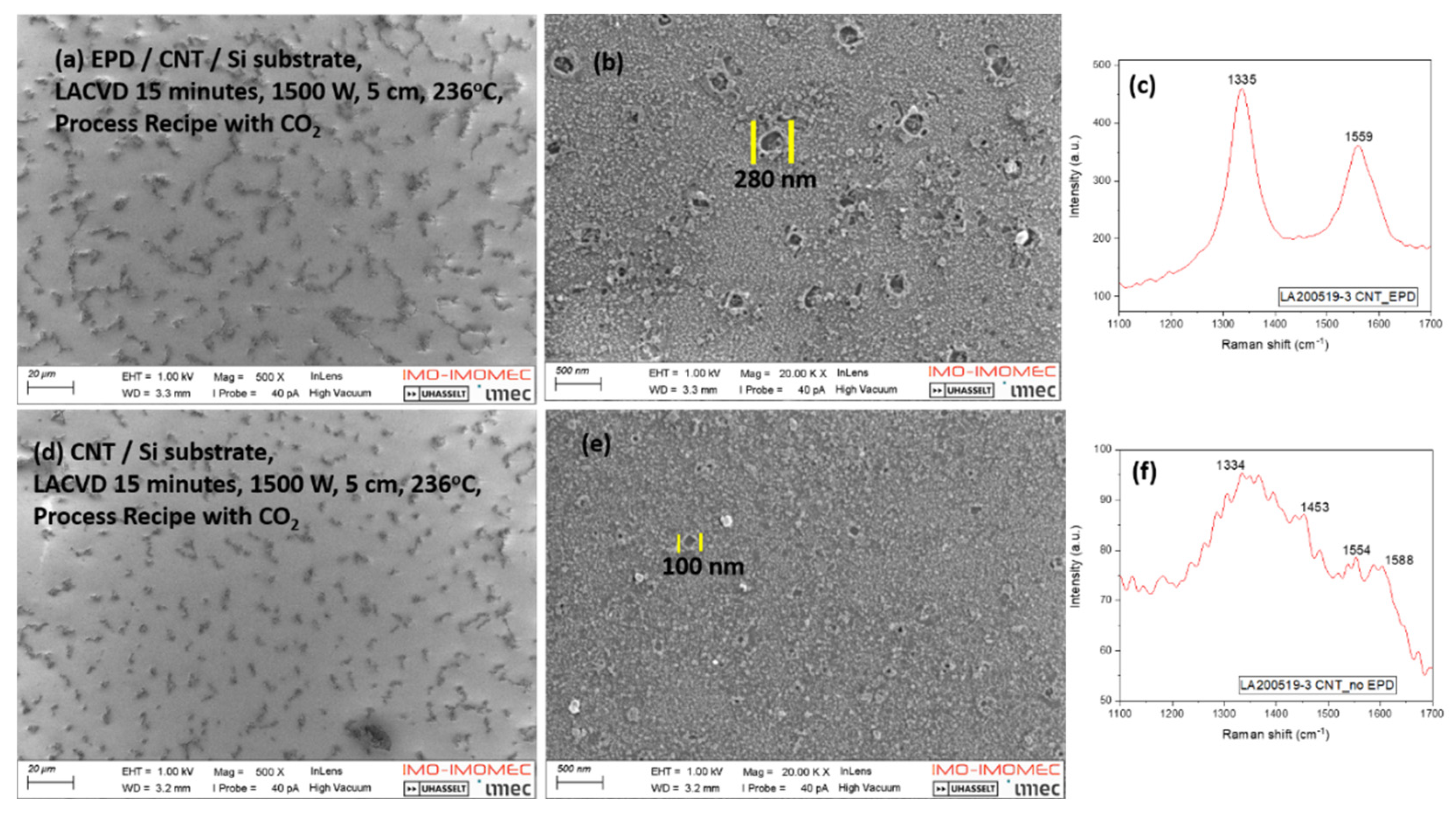
The SEM and Raman spectroscopy results from the CNT/Si and EPD-diamond/CNT/Si substrates kept alongside the silicon and sapphire DND seeded substrates are shown in Figure 5, after 15 minutes of LA-MPCVD processing. Longer CVD growth periods of 30 and 60 minutes, were completely etching the CNTs due to the oxidation by the microwave plasma recipe of H2:CH4:CO2=89:5:6. The well connected CNT network shown in Figure 1c is found to be etched completely by the LA-MPCVD plasma even after 15 minutes into the deposition period, as shown in figures 5a and 5d. However, the EPD treated CNT/Si substrate is found to be less affected by the LA-MPCVD plasma, as the length of individual CNTs are found to be longer (>20 µm) in Figure 5a than that in Figure 5d (<5 µm). Figure 5b is the higher magnification image of Figure 5a, taken from the intermediate region of the individual CNTs. It shows that the substrate surface is fully covered with carbonaceous film. The Raman signal of such film is shown in Figure 5c with stronger sp3 signal at 1335 cm-1 along with another less intense peak at 1559 cm-1 for graphitic carbon. The image 5b consists of tiny individual NCD grains (20-60 nm) present all over the EPD-diamond/CNT/Si plasma treated surface along with square shaped holes (140-280 nm). Such rectangular or square holes are also present on the CNT/Si plasma treated surface (Figure 5e) but much smaller in sizes (50-100 nm). Correspondingly, the individual diamond nanoparticles that are present all over the substrate surface in Figure 5e, are also smaller in sizes (20-40 nm) than those found in Figure 5b. Similarly, the sp3 (1334 cm-1) and graphitic (1588 cm-1) carbon signals from the plasma treated CNT/Si surface (Figure 5f) are also weaker, along with the presence of peaks at 1453 cm-1 which is due to TPA. The presence of sp3 Raman signal from the LA-MPCVD plasma treated CNT/Si substrates confirms the fact that even without nanodiamond seeding it was possible to deposit NCD on top of CNTs.
There are few white particles that are found to be present inside the rectangular holes (Figure 5b and Figure 5e). The holes might have been created with the dislodgment of such white particles. Thus, it is found that the EPD treated CNTs are burnt to a less extent by the LA-MPCVD plasma (comparing Figure 5a and Figure 5b). Moreover, it is also possible to grow CVD diamond onto CNT/Si substrate without the need of nanodiamond seeding (Figure 5f).
Figure 5.
EPD-diamond /CNT/Si substrate after 15 minutes of LA-MPCVD plasma treatment, (a) SEM at 500X magnification, (b) 20kX magnification, (c) Raman signal. EPD-diamond CNT/Si substrate after 15 minutes of LA-MPCVD plasma treatment, (d) SEM at 500X magnification, (e) 20kX magnification, (f) Raman signal. CNT/Si substrate after 15 minutes of LA-MPCVD plasma treatment.
3.2. Low MW power
The substrate temperatures that can be achieved inside the LA-MPCVD reactor, solely by means of plasma heating, depends on the input MW power and also on the stage to antenna distances. Therefore, in the next set of experiments, the MW power was reduced to 1100 W and also the stage to antenna distances were varied from 5 to 6.5 cm in order to see its effect on the growth of nanodiamond crystals during the early periods of LA-MPCVD. The lowest possible substrate temperature (15 hours of deposition) that Izak et al. [14] could achieve was 250oC by lowering the input microwave power to 1200 W. They also used 1700 W and 2500 W of higher input MW powers. However, they did not mention the substrate to antenna distance used in their experiments. Reportedly [11,16,22] it is kept at 5-7 cm optimal distances to achieve 400-450oC stable substrate temperature by plasma heating. Closer distances like 4 cm could produce 550oC substrate temperatures. In order to achieve higher substrate temperatures (>600oC), it is usually done by resistive heater underneath the substrate.
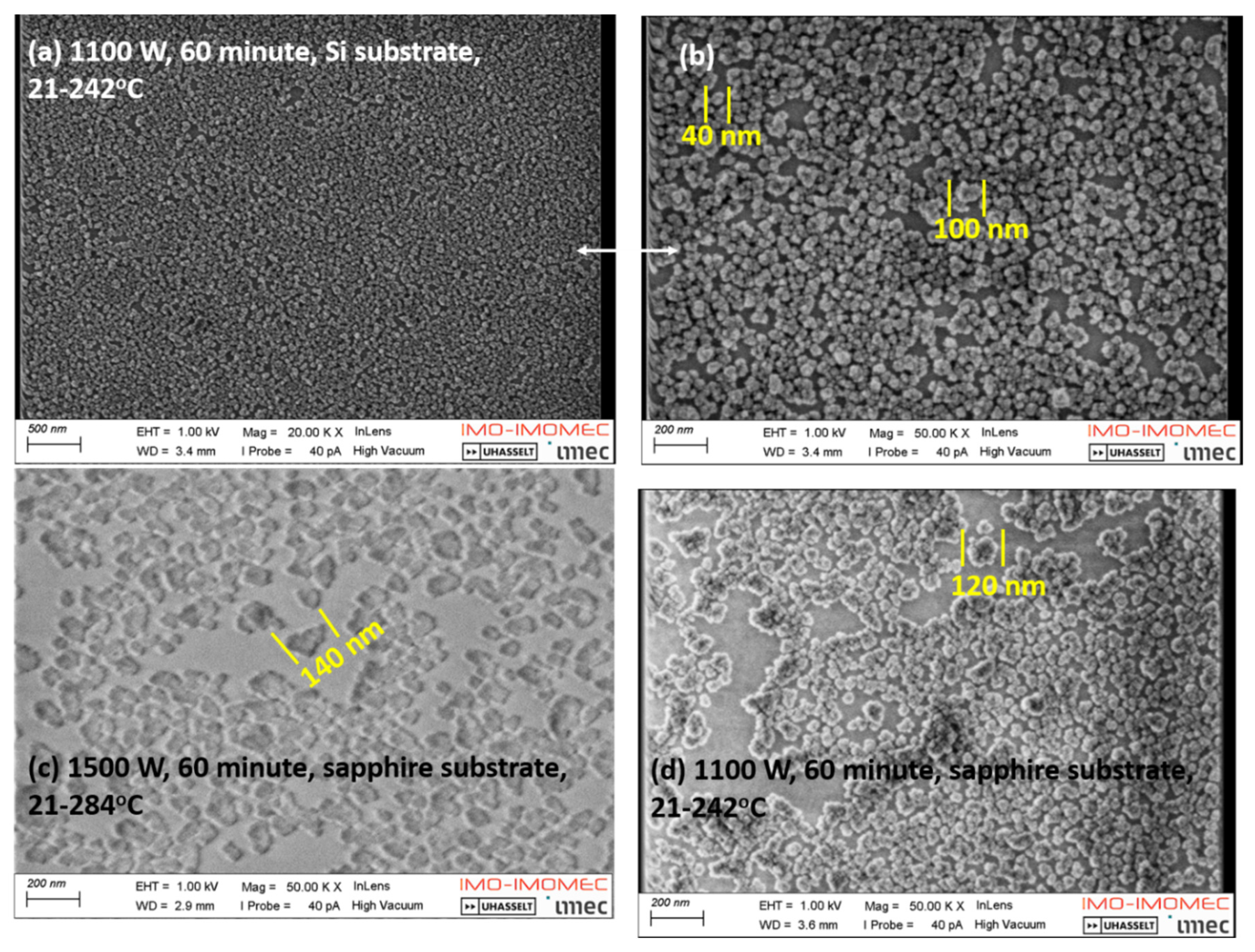
The substrate temperature continues to rise from the room temperature to 242oC, until the end of one-hour long LA-MPCVD run (Table 1, samples # LA200520-1). Surprisingly, at the lower MW of 1100 W, the NCDs were found to almost cover the entire silicon substrate (Figure 6a), which was not observed even at 1500 W (Figure 3d). Higher magnification SEM image in Figure 6b, reveals the NCD sizes to be around 40-100 nm. Still there are intermediate bare substrate areas visible in between the NCD grains. There is no evidence of secondary nucleation. The NCD seems to grow in lateral direction in order to cover the substrate surface by a single layer coalescing film.
Figure 6c (sapphire sample # LA200519-1) and Figure 6d (sapphire sample # LA200520-1) compare the effect of lowering the input MW power on the diamond growth behaviour during the first 60 minutes of LA-MPCVD processing with identical stage to antenna distance of 5 cm. 1500 W input MW power seems only to heat the substrate to a higher temperatures of 284oC, starting from room temperatures, but higher power did not help in effective grain coalescence - as it seems to be possible with 1100 W power as shown in Figure 6d. The sizes of the NCDs are comparable in between Figure 6c (approximately 140 nm NCDs scattered and isolated from each other) and 6d (about 120 nm NCD agglomerates). However, at lower power the grains are more coalesced and interconnected (Figure 6d). It appears that lower input power is beneficial to lateral growth of the diamond nanocrystals. There is still no sign of secondary-nucleation.
Figure 6.
Nearly coalesced NCD crystals grown by LA-MPCVD reactor at reduced power level of 1100 W on silicon substrate for 60 minutes, (a) 20kX and (b) 50kX magnification SEM images. Comparison of diamond nanocrystals coalescence on sapphire substrates after 60 minutes of LA-MPCVD at MW power levels of (c) isolated, at 1500 W and (d) connected, at 1100 W.
3.3. Pulse mode MW power
Pulse mode operation of LA-MPCVD reactor helps in achieving better quality diamond crystals with further reduction in input power level [13]. When the input MW power was 300 W, at 20 kHz pulse frequency and 45% duty cycles, the average output MW power recorded was 2000 W (Table 1). During the first hour LA-MPCVD run for the samples # LA200525-1, the substrate temperature continues to rise from room temperature to 290oC (similar to 1500 W, samples # LA200519-1) at a stage to antenna distance of 5 cm, however, after stopping the first run at the end of 60 minutes, the substrate was let to cool down to 140oC (reactor component safety temperature limit before opening the chamber door) before loading the second set of samples (# LA200525-2). Therefore, the starting temperature for the second run (# LA200525-2) was 126oC – it was not the room temperature, like it was for the previous first run (# LA200525-1). LA-MPCVD starting temperature of 126oC enables the substrate temperature to attain even higher value of 307oC after 60 minutes of plasma heating, even at a longer stage to antenna distance of 6.5 cm.
Figure 7 are the lower (5 kX - 7a and 7c) and higher magnification (50 kX - 7b and 7d) images of the silicon and sapphire substrates from the LA-MPCVD run # LA200525-1. It is found that pulse mode helped in producing denser film coverage of the silicon substrate (figures 7a and 7b) surfaces in comparison to 1500 W (# LA200519-1, Figure 3d) continuous mode input MW power runs after 1 hour of LA-MPCVD. However, if the figures 7a and 7c are compared, it appears that the sapphire substrates are more successfully covered (less contrasting black substrate areas) with diamond nanocrystals. But their respective higher magnification images reveal that the size of nanodiamonds are somewhat bigger (40-90 nm) on silicon substrates than that on the sapphire substrates (45-70 nm), and the respective grain size distribution is also narrower. The NCD sizes may be bigger for silicon substrates but their densities (≈7 NCDs on silicon against ≈12 NCDs on sapphire over 200 nm×200 nm substrate areas) are higher for the sapphire substrates – indicating favourable growth on the sapphire substrates. But still, the pulse mode could not produce continuous NCD films on both the substrates. The primary reason is the unstable (continuously rising, 21o – 290oC) substrate temperature, which did not allow to grow nanodiamond crystals, fully covering the substrate surface.
3.4. Fully coalesced NCD films
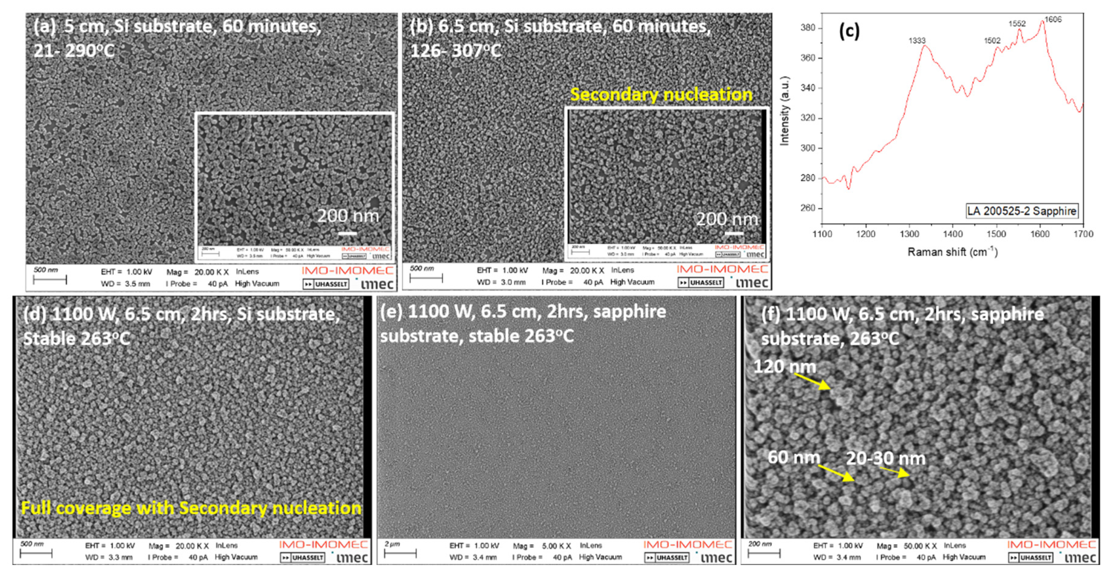
It was found, that, even after 60 minutes of LA-MPCVD processing, at higher power of 1500 W, or lower power of 1100 W, or even with pulse mode MW power, at a stage to antenna distance of 5 cm, none of the processing conditions, could produce continuous diamond films on both the DND seeded silicon and sapphire substrates. Had this been conventional resonant cavity microwave plasma CVD reactor, it would have produced continuous micron thick high quality NCD films with H2/CH4/CO2 = 89/5/6 process recipe after 1 hour of growth [1]. Next, it was attempted to lower the substrate stage to 6.5 cm distance away from the linear antenna quartz tube, in order to lower the substrate temperature. In effect, it was as to promote less etching of the deposited films nearer to the antenna, and producing a continuous film formation on the substrate surface - even if it will be poorer in diamond quality.
Lowering the stage from 5 cm to 6.5 cm is beneficial to the substrate surface. Figure 8a and its inset which were the diamond film SEM images on silicon substrate after 1 hr LA-MPCVD in pulse mode at 5 cm distance, still show dark contrasting uncovered silicon substrate areas underneath, but the nanodiamond grains are more or less connected with each other without any sign of isolated NCDs. It appears from the Figure 8a that the pulse mode was more effective processing condition in covering the substrate surface with single layer of NCD film. But if the distance is increased to 6.5 cm (Figure 8b and inset), there is sign of secondary nucleation which may produce poor quality diamond. It concludes that wider stage to antenna distance helped in secondary nucleation to take place and produced almost fully covered silicon substrate. The Raman signal from such semi-continuous NCD film on sapphire substrate shows very high FWHM of 40 cm-1 for the sp3 peak at 1333 cm-1, along with appearance of TPA peak at 1502 and graphite G peaks at 1606 and 1552 cm-1. The high value of FWHM confirms the presence of secondary nuclei, as evident also from the SEM image. The end temperature of the second 60-minute LA-MPCVD run was somewhat higher at 307oC, as its starting temperature was also higher at 126oC - after the end of first experiment of 60 minutes LA-MPCVD which started from room temperature of 21oC. But both of them were not performed long enough to make the substrate temperature reaching a stable flat curve. The substrate temperature was continuously changing (increasing) during both the runs – initially at a faster pace (steep slope) and later on at slower (flatter slope) heating rates.
It was found that for the samples # LA200520-2, grown at longer substrate to antenna distance of 6.5 cm, and grown for longer duration of 2 hrs, LA-MPCVD process conditions could produce a flat substrate temperature curve as shown in Figure 2c. The longer distance of 6.5 cm promoted in producing secondary nucleation of diamond crystals (wide range of NCD grain sizes from 20-120nm – Figure 8f) and longer time of LA-MPCVD allowed the films to coalesce to form full substrate coverage as shown in figures 8d-f. Earlier it was also found that lower power of 1100 W contributed to produce better film coverage (Figure 6a) than 1500 W on silicon substrate (Figure 3a). Figure 6d is the NCD film after 1 hr LA-MPCVD on sapphire, showing underlying bare substrate but if the LA-MPCVD was allowed to proceed for another 1 hr, it was found to fully cover the sapphire substrate surface (Figure 8e and Figure 8f). Figure 6d shows a cluster of 12 diamond nanoparticles, with 120 nm total diameter. Although every grain is not of equal dimension, but it may be estimated that the individual nanodiamond crystals are 5-10 nm in size. This was the case after 1 hr of LA-MPCVD on sapphire substrate, but when the LA-MPCVD was proceeded for another 60 minutes, it is found to produce secondary nucleation with variable nanodiamond sizes of 120, 60 or 30 nm of individual grain sizes (Figure 8f). Therefore, longer periods of LA-MPCVD helped to grow the film both laterally and in three dimensions due to secondary nucleation. Researchers have earlier reported [22] that there are high pressure growth regime which promotes diamond re-nucleation and low pressure growth regime which promotes lateral growth. Low electron temperature inside LA-MPCVD is essential for continuous re-nucleation of diamond in hydrogen rich plasma [42].
Figure 8.
Coalescence and secondary nucleation of NCDs. SEM of (a) interconnected NCD on Si, pulse mode at 5 cm, (b) secondary nucleated NCDs on Si in pulse mode at 6.5 cm, (c) Raman spectra from secondary nucleated NCD after 1 hr LA-MPCVD in pulse mode at 6.5 cm. SEM images of NCDs after 2 hr LA-MPCVD in CW mode at 6.5 cm, 1100 W power (d) on Si, (e) sapphire substrates and (f) 50 kX magnification of image in 8e.
3.5. LA-MPCVD growth without CO2
3.5.1. EPD-diamond/CNT/Si substrates
It was found that the EPD treated CNT/Si substrates were also etching out fast under the LA-MPCVD plasma recipe of H2:CH4:CO2=89:5:6. Therefore, in order to reduce the effect of oxidation, in the next set of experiments, CO2 gas was removed from the process recipe. Figure 9a and 9b show the Raman spectra of the EPD seeded CNT/Si substrates after 15 and 30 minutes of LA-MPCVD plasma treatment without CO2 in the recipe of H2:CH4=97:3. It was found that even after 30 minutes of LA-MPCVD, CNT survived the plasma conditions (inset Figure 9d). The corresponding Raman signal of the sp3 peak was weaker than those of the graphitic D-band (Figure 9a) after 15 minutes of LA-MPCVD, however, the Raman spectra started producing fluorescent signals after 30 minutes of LA-MPCVD as shown in Figure 9b. There lies a definitive signal (not prominent enough due to background fluorescence) for diamond at 1330 cm-1 which was taken from the sample in Figure 9d. There are loosely scattered diamond nanoparticles, of around 80 nm diameter or less, all throughout the images in 9c and 9d. There is some occasional appearance of square or rectangular holes in the plasma treated EPD-diamond/CNT/Si substrate surface. Sizes of those holes vary from 250-350 nm. It is interesting to see that some of the holes were occupied by bright whitish nanoparticles - its dimensions was measured to be 250 nm. It can be assumed that dislodgment of such white particles resulted in the creation of those square or rectangular holes. The SEM images of figures 9c and 9d were taken from the intermediate regions of the individual CNTs (inset image of Figure 9d). The sizes of the some of the CNTs are found to be as big as 25 µm. If the CNT lengths in Figure 9d are compared with those in figures 5a (20 µm after15 minutes LA-MPCVD), it is concluded that even after 30 minutes of LA-MPCVD plasma treatment, EPD seeded CNT/Si survived diamond deposition conditions without complete etching, due to the absence of CO2 in the recipe.
3.5.2. Silicon and sapphire substrates
3.5.2. a. Effect of CH4
Section 3.1.1. and Section 3.1.2. have already shown that the early periods of low temperature LA-MPCVD run could not produce fully covered, otherwise perfectly DND seeded silicon and sapphire substrates (even after 60 minutes of deposition). One of the reasons of the slow growth of diamond crystals, could have been rapid etching of the nanodiamond films by the CO2 present in the plasma recipe. Therefore, it was further investigated to see the effect of removing CO2 from the recipe during the LA-MPCVD nanodiamond growth. Researchers [43] have shown that at the low CO2 concentration (less than 0.5%), there is formation of SiC in competition with the growth of boron doped NCD during the LA-MPCVD process, which is due to the silicon contamination from the quartz tube. Moreover CO2 (less than 1%) enhances the NCD growth rate (16 nm/hr) in continuous mode LA-MPCVD. But an increase in CO2 gas over CH4 gas percentages reduced [11,13] the growth rate (7 nm/hr). But there is no report so far about the effect of CH4 percentages on the NCD growth pattern, specifically during the unstable periods of LA-MPCVD run, i.e., until the stable substrate temperature is achieved.
Figure 10a, Figure 10b and Figure 10c are the SEM images of the NCD crystals grown over the Si substrates with the increasing methane percentages (3% - 5%), only after first 15 minutes of LA-MPCVD. It is found that the individual DND seed crystals (Figure 1a) grew in sizes in figures 10. The diamond nanoparticle density is calculated to be equal to 0.85×10¹⁰/cm2 in figures 11c for 5% CH4 percentage over silicon substrates, to some extent less than the that calculated from the Figure 1a for the DND seeds (2×10¹⁰/cm2). It demonstrates that during the early growth stage, the DND seeds only grow laterally in size, also with the disappearance of some seed crystals due to plasma etching. The Raman signal from the NCD film on Si substrate, grown at 3% CH4, but after 30 minutes of LA-MPCVD (Figure 10d), is shown to produce quite sharp sp3 peak with FWHM of 22 cm-1. There are also Raman peaks in the Figure 10d corresponding to non-diamond carbon depositions at 1541 and 1600 cm-1, respectively. It is observed that the dark contrasting Si substrate areas in the figures 10a, 10b and 10c are progressively diminished - indicating that with the increase in the CH4 percentages, the DND seed crystals grow bigger in sizes, within a given LA-MPCVD time period.
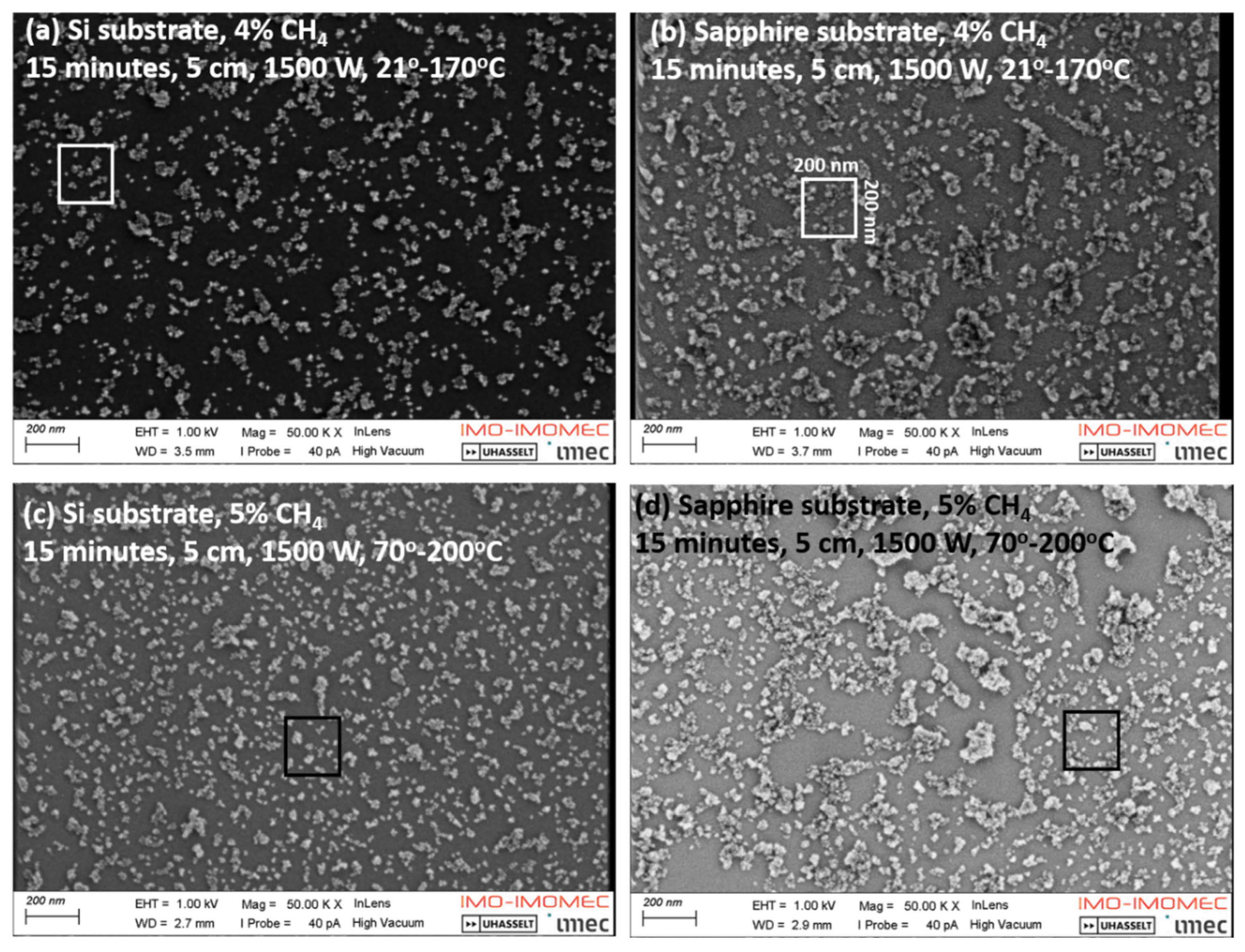
If the NCD crystal densities are compared in between silicon and sapphire substrates after 15 minutes of LA-MPCVD growth at 4% CH4 without CO2 (Figure 11a and 11b), it is found that there are 10 NCDs within an area of 200 nm × 200 nm square (Figure 11a) on Si and there are about 20 NCDs on sapphire substrate (Figure 11b). Hence it may be inferred that sapphire substrates are more effective in growing the DND seeds. Similar trend of double the number of NCD crystals present on the sapphire substrate in comparison to the silicon substrate after the 15 minutes of LA-MPCVD growth, at 5% CH4 without CO2 (Figure 11c and Figure 11d), is also observed.
Now if we compare the NCD crystal densities onto Si substrate with increasing CH4 percentages, it is observed that there are more NCDs, 15 in number, within an area of 200 nm × 200 nm square (Figure 11c). Similarly increase in CH4 percentages from 4% to 5% on the sapphire substrate also increases the NCD crystal densities from 20 to 30 NCDs present within an area of 200 nm × 200 nm square (Figure 11b and Figure 11d) of the sapphire substrate after 15 minutes of LA-MPCVD growth. Thus, it can be concluded that the increasing methane percentages promoted LA-MPCVD growth of NCDs.
Figure 10.
LA-MPCVD growth of NCD crystals on DND seeded silicon substrates without CO2 in the recipe. SEM images showing early stages of CVD diamond growth at (a) 3%, (b) 4% and (c) 5% CH4 after 15 minutes of growth at 1500 W input average power. (d) Raman signal from such NCD crystals.
Figure 10.
LA-MPCVD growth of NCD crystals on DND seeded silicon substrates without CO2 in the recipe. SEM images showing early stages of CVD diamond growth at (a) 3%, (b) 4% and (c) 5% CH4 after 15 minutes of growth at 1500 W input average power. (d) Raman signal from such NCD crystals.
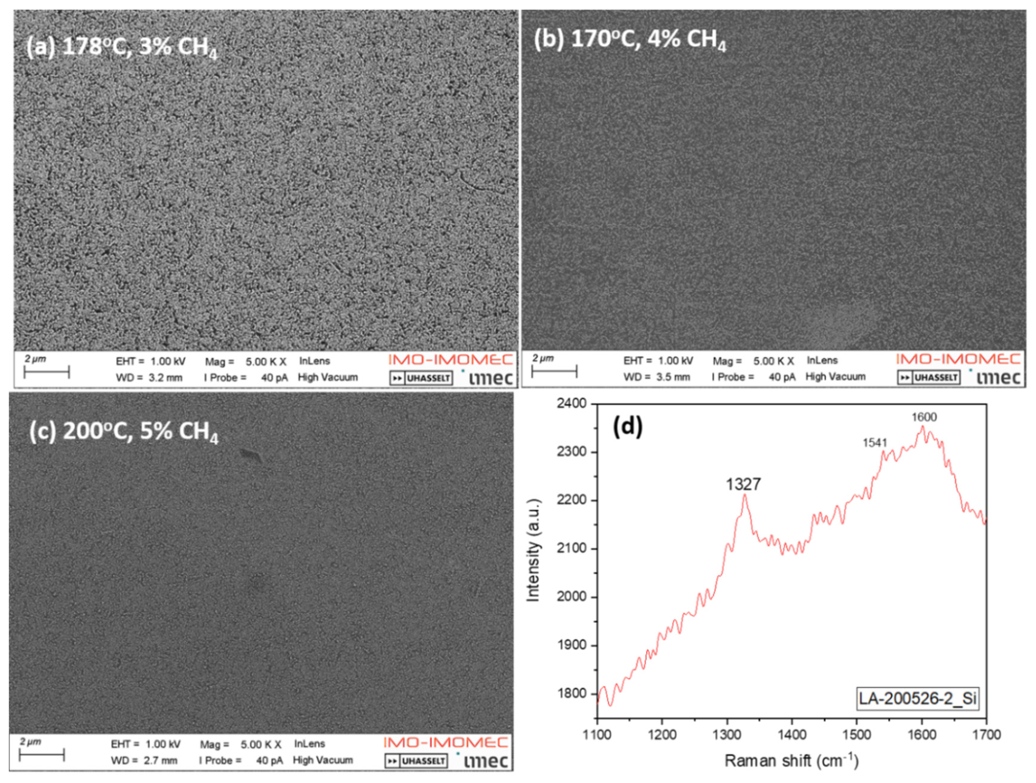
Figure 11.
Comparison of LA-MPCVD growth (1500 W, 5 cm, 15 minutes) of NCD crystals on DND seeded silicon and sapphire substrates without CO2 in the recipe. NCD crystal (samples # LA200605-1) SEM 50 kX magnification images on (a) Si and (b) sapphire substrates at 4% CH4. NCDs (samples # LA200605-2) on (c) Si and (d) sapphire substrates at 5% CH4.
3.5.2. b. Effect of deposition time
Growth rates of linear antenna CVD is slower in comparison to conventional microwave plasma CVD growth of diamond crystals inside resonant cavity reactors. The typical growth rates for MPCVD is in the order of microns per hour [1,44], whereas inside LA-MPCVD, NCD grows by 5-20 nm per hour [13] - depending on the presence of CO2 percentages in the recipe and also on the use of pulse mode, which favours higher growth rates. Hence, it is understood that longer LA-MPCVD deposition time is required to fully cover the substrates NCD films. The available literature reports only about the long deposition periods (mostly 8, 15 and 20 hours of LA-MPCVD). There is little or no information about the growth of NCDs during the initial periods of LA-MPCVD, when the substrate temperature is not stabilised yet (Figure 1a) and is continuously increasing by heating with plasma. Figure 1b is the cooling-heating cycle for the samples # LA200605-3, with 11 minutes of short LA-MPCVD deposition period, shown with a sudden rise in substrate temperature (from 88o to 270oC) at 2800 W input average power and 5 cm stage to antenna distance. The experiment # LA200605-1 started from the room temperature with 4% CH4 and the plasma heating lasted for 15 minutes, which continuously increased the substrate temperature up to 170oC at 1500 W input average power and at 5 cm stage to antenna distance. Thereafter, the reactor was let to cool down below 140oC (temperature-safety-limit of the reactor) before it was to re-open to unload and reload the next set of 4-substrates. In this way, the starting temperature for the next set of samples # LA200605-2 became 70oC (not restarting from the room temperature) and again with 15 minutes of heating with 5% CH4 in the hydrogen plasma, it could heat up to a little bit of higher substrate temperature of 200oC at 1500 W input average power and 5 cm stage to antenna distance. Again, the experiment was stopped and the reactor was allowed to cool down to 88oC (shown in Figure 1b – depending on the time one takes to load and unload samples) before restarting # LA200605-3 for 11 minutes of plasma heating up to 270oC, but at 2800 W power and 5 cm distance. The important point to be noticed is that the heating rates were, 9.9 oC/min for # LA200605-1, 8.6 oC/min for # LA200605-2, and 16.5oC/min for # LA200605-3. The third LA-MPCVD heating rate was higher because of the very high input MW power level of 2800 W.
Figure 12a and Figure 12c compare the diamond film growth behaviour on silicon substrates after 15 min. (1500 W) and 11min. (2800 W) of LA-MPCVD heating with 5% CH4 in the hydrogen plasma recipe, respectively. There are almost equal numbers (about 45 diamond nanoparticles inside 500 nm × 500 nm square) of whitish bright NCD particles scattered on the dark contrasting silicon substrate in both the images. Although, there was a 4-minute reduction in deposition time with concomitant increase in MW input power by 1300 W, the Figure 12c shows somewhat sharper white spots of NCDs on Si, which may be due to its wider substrate temperature range of 88o-270oC. On the other hand, sapphire substrate has more numbers (approximately 70 diamond nanoparticles inside 500 nm × 500 nm square) of NCDs scattered in the Figure 12b. Moreover, there are also signs of nanodiamond agglomeration in Figure 12b. It may be concluded that sapphire substrate favoured more lateral growth of DND seed crystals than silicon substrate. It may be attribute to a tendency for silicon to form carbide which reduces the formation of diamond nanoparticles. The number of NCD particles present inside 200 nm × 200 nm square area is about 20 in the Figure 12d, for the LA-MPCVD growth on sapphire substrate, for 11 minutes with 5% CH4 at 2800 W power and at 5 cm distance - which is almost equal in number of the NCD particle density found in Figure 11b for 15 minutes of LA-MPCVD with 4% CH4 at 5 cm distance. The number of diamond nanoparticles was 30 in Figure 11d inside 200 nm × 200 nm square area for 15 minutes of LA-MPCVD with 5% CH4 at 5 cm distance. So, this decrease in NCD density number (30 to 20) with identical LA-MPCVD recipe is mainly due to the decrease in deposition time from 15 to 11 minutes. It is important to note that although the MW input power was much higher (2800 W) - leading to higher substrate temperatures (88o-270oC), but it could not become effective in increasing the diamond nanoparticle density at shorter LA-MPCVD periods of 11 minutes.
Now, if the LA-MPCVD was allowed to proceed from 15 minutes to 30 minutes at 3% CH4 in the process recipe without CO2, with simultaneous lowering of the stage from 5 to 6.5 cm distance away from the quartz tube antenna, it was found (inside 500 nm × 500 nm squares) that the NCD crystal sizes grow bigger in sizes with concomitant touch with each other to form some kind of agglomeration (Figure 13a and Figure 13c) on silicon substrate surfaces. On the other hand, the NCD crystals are found already to be much bigger on sapphire substrates (Figure 13b and Figure 13d) under identical LA-MPCVD processing conditions than on the silicon substrates, which is again due to tendency of silicon to form carbide favourably over nanodiamond formation. There are about 15 NCD crystals/agglomerates inside 200 nm × 200 nm squares in Figure 13b in comparison to approximately 10 NCD crystals/agglomerates inside 200 nm × 200 nm squares in Figure 13d. The NCD sizes vary from as small as 25 nm individual crystals to as big an agglomeration size as 100 nm in Figure 13d, whereas, the smallest NCD in Figure 13b is about 20 nm and the biggest agglomeration is found to be as big as 50-60 nm. Therefore, it may be concluded that longer deposition time allowed the NCD to grow in the lateral direction in covering more the underlying sapphire substrate, gradually with time. The NCD crystals are found to be 40-45 nm in size (Figure 13c) on silicon substrate after 30 minutes of LACVD with 3% methane in hydrogen plasma, occasionally touching each other, whereas, in Figure 13a (15 minutes) they remained isolated from each other with smaller (30 – 35 nm) diamond nanoparticle sizes.
4. Conclusion
Early period growth of NCD crystals inside LA-MPCVD reactor has been presented, during the initial temperature rise of the substrates by microwave plasma heating. It has been observed that the substrate temperature keeps on increasing during the first hours of LA-MPCVD and the NCD film remains discontinuous on the DND seeded silicon and sapphire substrates. Although, the short duration LA-MPCVD runs for 15 minutes were not effective in coalescing the NCD films, but it was found appropriate for coating CNT with NCD. The CNT/Si samples were found to be severely etched out (<5 µm) under H2:CH4:CO2=89:5:6 plasma recipe - more than the EPD treated CNT/Si substrates (>20 µm). Pre-treatment with electrophoretic diamond seeds helped in protecting the carbon nanotubes from plasma etching as evident from their longer CNT lengths after 15 minutes of LA-MPCVD runs. Further prevention of plasma etching of the EPD seeded CNT/Si substrate was observed without CO2 gas in the LA-MPCVD process recipe, with the evidence of 25 µm long CNTs present even after 30 minutes of LA-MPCVD runs.
On the other hand, the DND seeded sapphire substrates were found to favour the formation of bigger (120 nm) NCD particles, than (100 nm) silicon substrates which has a tendency to form carbide, during 60 minutes LA-MPCVD at reduced power level of 1100 W. Sapphire also showed to favour the formation of higher NCD particle densities - almost double the number of diamond nanoparticles within 200 nm × 200 nm substrate areas, under identical LA-MPCVD processing conditions, than silicon. With increase in deposition time from 15 to 60 minutes, the NCDs grow bigger in size along the lateral direction, gradually starting to cover the entire DND seeded substrates. But LA-MPCVD of 1 hr was not enough to completely coalesce the diamond films. The Raman signals were better (FWHM of sp3 = 18 cm-1) from longer period (60 minutes) LA-MPCVD run samples than shorter duration LA-MPCVD samples, as the amount of nanodiamond crystals that are present on the substrate surface, increases with deposition time - allowing better detection of the respective Raman signals. Moreover, the Raman signals were also found to be relatively better from sapphire substrates (FWHM of sp3 = 15 cm-1) than from the NCDs on silicon substrate, under identical LA-MPCVD parameters. Lowering of the input microwave power level from 1500 to 1100 W in continuous wave mode, favoured the formation of connected 40-100 nm sized NCDs (on Si) – thereby nearly covering the DND seeded silicon and sapphire substrates. On the other hand, pulse mode LA-MPCVD experiments also found to help in improving the NCD crystal formation with bigger grain sizes (40-90 nm on Si) and more effective surface coverage of the substrates. Increasing the stage to antenna distance from 5 cm to 6.5 cm promoted in the formation of secondary nucleation sites. Re-nucleation at longer substrate to quartz tube distances, along with, longer deposition time of 2 hr, are found to be essential in growing continuous NCD films. However due to secondary nucleation, the corresponding Raman sp3 peak had much wider FWHM of 40 cm-1 value. The effect of increasing CH4 percentages in the process recipe was to supply more carbon atoms necessary for increasing the densities of diamond nanoparticles on DND seeded substrates. It was also found that the NCD crystal densities were higher on sapphire substrates than on the silicon substrates under identical LA-MPCVD conditions of process recipe without CO2 gas. Deposition time is the most important factor for NCD growth during the early stages of LA-MPCVD. Even a higher input power of 2800 W (therefore higher temperatures) could not significantly affect the NCD crystal sizes within short periods of time. With 3% CH4 in 97% H2 in the process recipe and at a 5 cm stage to antenna distance, it was found that 4-6 nm DND seed crystals on Si substrates grew into about 30 nm sizes of diamond nanoparticles after 15 minutes of LA-MPCVD and into about 45 nm sizes of diamond nanoparticles after 30 minutes of LA-MPCVD. Whereas, 60 minutes of LA-MPCVD at a lower input power of 1100 W could produce 100 nm sized nanodiamond agglomerations with semi-continuous NCD film on Si, with H2:CH4:CO2=89:5:6 plasma recipe. It was necessary to run the LA-MPCVD experiments long enough (2 hrs) to achieve a flat stable substrate temperature (263oC) and also it was effective to lower the distance (6.5 cm) away from the antenna to enable re-nucleation of the diamond nanoparticles - essential for rapid growth of nanodiamond particles.
Author Contributions
AKM: conceptualization, methodology, formal analysis, investigation, resources, data curation, writing—original draft preparation, writing—review and editing, visualization; WCS: conceptualization, methodology, formal analysis, investigation, resources, data curation, writing—review and editing, visualization; PP: conceptualization, methodology, formal analysis, investigation, resources, data curation, writing—review and editing, visualization; KH: conceptualisation, validation, writing—review and editing, visualisation, supervision, project administration, funding acquisition.
Funding
This work was financially supported by the Methusalem NANO network and the Research Foundation – Flanders (FWO) via project G0D4920N. AKM acknowledges FWO for his Postdoctoral Fellowship with grant no. 12X2919N.
Acknowledgments
All data generated or analysed during this study are included in this published article. The datasets generated during and/or analysed during the current study are available from the corresponding author on reasonable request.
Conflicts of Interest
The authors declare that they have no known competing financial interests or personal relationships that could have appeared to influence the work reported in this paper.
References
- A. Grotjohn, J. Asmussen, Microwave Plasma-Assisted Diamond Film Deposition, Chapter 7, Diamond Films Handbook, edited by J. Asmussen and D. K. Reinhard, published by Marcel Dekker, Inc. (2002).
- Das, R. N. Singh, A review of nucleation, growth and low temperature synthesis of diamond thin films, International Materials Reviews. 2007, 52, 29–64.
- Piazza , G. Morell, Synthesis of diamond at sub 300 °C substrate temperature, Diamond and Related Materials. 2007, 16, 1950–1957.
- Ihara, H. Macho, and H. Komiyama, Low-temperature deposition of diamond in a temperature range from 70 °C to 700 °C, Diamond and Related Materials. 1992, 1, 187.
- Potocky, A. Kromka, M. Vanecek, Growth of nanocrystalline diamond films deposited by microwave plasma CVD system at low substrate temperatures, Physica Status Solidi A. 2006, 203, 3011.
- Gueroudji and N. M. Hwang, Thermodynamic limits for the substrate temperature in the CVD diamond process, Diamond and Related Materials. 2000, 9, 205–211. [CrossRef]
- Gu, Z. Chen, R. Li, X. Zhao, C. Das, V. Sahmuganathan, J. Sudijono, M. Lin, K. P. Loh, Nanocrystalline diamond film grown by pulsed linear antenna microwave CVD, Diamond and Related Materials. 2021, 119, 108576. [CrossRef]
- Tsugawa, M. Ishihara, J. Kim, M. Hasegawa and Y. Koga, Large-Area and Low-Temperature Nanodiamond Coating by Microwave Plasma Chemical Vapor Deposition, New Diamond and Frontier Carbon Technology. 2006, 16, 337–346.
- Marton, M. Vojs, P. Michniak, M. Behúl, V. Rehacek, M. Pifko, Š. Stehlík, A. Kromka, New chemical pathway for large-area deposition of doped diamond films by linear antenna microwave plasma chemical vapor deposition, Diamond and Related Materials. 2022, 126, 109111. [CrossRef]
- Kromka, O. Babchenko, T. Izak, K. Hruska, B. Rezek, Linear antenna microwave plasma CVD deposition of diamond films over large areas, Vacuum. 2012, 86, 776–779. [CrossRef]
- Fendrych, A. Taylor, L. Peksa, I. Kratochvilova, J. Vlcek, V. Rezacova, V. Petrak, Z. Kluiber, L. Fekete, M. Liehr, M. Nesladek, Growth and characterization of nanodiamond layers prepared using the plasma-enhanced linear antennas microwave CVD system, Journal of Physics D: Applied Physics. 2010, 43, 374018. [CrossRef]
- Potocky, O. Babchenko, K. Hruska, A. Kromka, Linear antenna microwave plasma CVD diamond deposition at the edge of no-growth region of C–H–O ternary diagram, Physica Status Solidi B. 2012, 249, 2612–2615. [CrossRef]
- Taylor, F. Fendrych, L. Fekete, J. Vlček, V. Řezáčová, V. Petrák, J. Krucký, M. Nesládek, M. Liehr, Novel high frequency pulsed MW-linear antenna plasma-chemistry: Routes towards large area, low pressure nanodiamond growth, Diamond and Related Materials. 2011, 20, 613–615. [CrossRef]
- Izak, O. Babchenko, M. Varga, S. Potocky, A. Kromka, Low temperature diamond growth by linear antenna plasma CVD over large area, Phys. Status Solidi B. 2012, 249, 2600–2603. [CrossRef]
- Drijkoningen, P. Pobedinskas, S. Korneychuk, A. Momot, Y. Balasubramaniam, M. K. Van Bael, S. Turner, J. Verbeeck, M. Nesládek, K. Haenen, On the Origin of Diamond Plates Deposited at Low Temperature, Crystal Growth Design. 2017, 17, 4306–4314. [CrossRef]
- J. Mistrik, P. Janicek, A. Taylor, F. Fendrych, L. Fekete, A. Jager, M. Nesladek, Spectroscopic ellipsometry characterization of nano-crystalline diamond films prepared at various substrate temperatures and pulsed plasma frequencies using microwave plasma enhanced chemical vapor deposition apparatus with linear antenna delivery, Thin Solid Films. 2014, 571, 230–237. [CrossRef]
- Tsugawa, M. Ishihara, J. Kim, Y. Koga, M. Hasegawa, Nanocrystalline diamond film growth on plastic substrates at temperatures below 100°C from low-temperature plasma, Physical Review B. 2010, 82, 125460.
- Neykova, H. Kozak, M. Ledinsky, A. Kromka, Novel plasma treatment in linear antenna microwave PECVD system, Vacuum. 2012, 86, 603–607.
- Bénédic, M Belmahi, T Easwarakhanthan, P Alnot, In situ optical characterization during MPACVD diamond film growth on silicon substrates using a bichromatic infrared pyrometer under oblique incidence, Journal of Physics D: Applied Physics. 2001, 34, 1048.
- J. J. Gracio, Q. H. Fan, J. C. Madaleno, Diamond growth by chemical vapour deposition. Journal of Physics D: Applied Physics. 2010, 43, 374017.
- Kromka, Š. Potocký, J. Čermák, B. Rezek, J. Potměšil, J. Zemek, M. Vaněček, Early stage of diamond growth at low temperature, Diamond & Related Materials. 2008, 17, 1252–1255.
- Babchenko, Š. Potocký, T. Ižák, K. Hruška, Z. Bryknar, A. Kromka, Influence of surface wave plasma deposition conditions on diamond growth regime, Surface & Coatings Technology. 2015, 271, 74–79.
- Bai, Y. Wang, T. I. Feygelson, M. J. Tadjer, K. D. Hobart, N. J. Hines, L. Yates, S. Graham, J. Anaya, M. Kuball, M. S. Goorsky, Diamond Seed Size and the Impact on Chemical Vapor Deposition Diamond Thin Film Properties, ECS Journal of Solid State Science and Technology. 2020, 9, 053002.
- Pobedinskas, S. D. Janssens, J. Hernando, P. Wagnera, M. Nesládek, K. Haenen, Selective seeding and growth of nanocrystalline CVD diamond on non-diamond substrates, MRS Proceedings. 2011, 1339.
- Pobedinskas, G. Degutis, W. Dexters, W. Janssen, S. D. Janssens, B. Conings, B. Ruttens, J. D’Haen, H.-G. Boyen, A. Hardy, M. K. Van Bael, K. Haenen, Surface plasma pretreatment for enhanced diamond nucleation on AlN, Applied Physics Letters. 2013, 102, 201609.
- Z. Rotter, J. C. Madaleno, Diamond CVD by a combined plasma pretreatment and seeding procedure, Chemical Vapor Deposition. 2009, 15, 209–216.
- sugawa, M. Ishihara, J. Kim, Y. Koga, and M. Hasegawa, Nucleation Enhancement of Nanocrystalline Diamond Growth at Low Substrate Temperatures by Adamantane Seeding, The Journal of Physical Chemistry C. 2010, 114, 3822–3824.
- Arnault, L. Demuynck, C. Speisser, F. L. Normand, Mechanisms of CVD diamond nucleation and growth on mechanically scratched Si(100) surfaces, The European Physical Journal B-Condensed Matter and Complex Systems. 1999, 11, 327–343.
- G. Buijnsters, L. Vázquez, J. J. ter Meulen, Substrate Pre-Treatment by Ultrasonication with Diamond Powder Mixtures for Nucleation Enhancement in Diamond Film Growth, Diamond and Related Materials. 2009, 18, 1239–1246.
- Shenderova, S. Hens, G. McGuire, Seeding slurries based on detonation nanodiamond in DMSO, Diamond and Related Materials. 2010, 19, 260–267.
- Domonkosa, T. Ižák, M. Varga, Š. Potocký, P. Demo, A. Kromka, Diamond nucleation and growth on horizontally and vertically aligned Si substrates at low pressure in a linear antenna microwave plasma system, Diamond and Related Materials. 2018, 82, 41–49.
- M. Affoune, B. L. V. Prasad, H. Sato, T. Enoki, Electrophoretic Deposition of Nanosized Diamond Particles, Langmuir. 2001, 17, 547–551.
- Tsubota, S. Ida , N. Okada , M. Nagata , Y. Matsumoto, N. Yatsushiro, CVD diamond coating on WC–Co cutting tool using ECR MPCVD apparatus via electrophoretic seeding pretreatment, Surface and Coatings Technology. 2003, 169–170, 262–265.
- Chang, K. Panda, B. K. Panigrahi, S. Lou, C. Chen, H. Chan, I. Lin, N. Tai, Electrophoresis of Nanodiamond on the Growth of Ultrananocrystalline Diamond Films on Silicon Nanowires and the Enhancement of the Electron Field Emission Properties, Journal of Physical Chemistry C. 2012, 116, 19867–19876.
- J.W. Smith, A.H. Piracha, D. Field, J.W. Pomeroy, G.R. Mackenzie, Z. Abdallah, F.C.-P. Massabuau, A.M. Hinz, D.J. Wallis, R.A. Oliver, M. Kuball, P.W. May, Mixed-size diamond seeding for low-thermal-barrier growth of CVD diamond onto GaN and AlN, Carbon. 2020, 167, 620–626.
- Potocký, M. Cada, O. Babchenko, T. Ižák, M. Davydova, A. Kromka, Perspectives of linear antenna microwave system for growth of various carbon nano-forms and its plasma study, Physica Status Solidi B. 2013, 250, 2723–2726.
- Potocký, O. Babchenko, M. Davydova, T. Izak, M. Čada, A. Kromka, Growth of carbon allotropes and plasma characterization in linear antenna microwave plasma CVD system, Japanese Journal of Applied Physics. 2014, 53, 05FP04.
- Zou, P. W. May, S. M. C. Vieira, N. A. Fox, Field Emission from Diamond-Coated Multiwalled Carbon Nanotube “Teepee” Structures. Journal of Applied Physics. 2012, 112, 044903.
- Chang, S. Kunuku, Y. Hong, K. Leou, T. Yew, N. Tai, I. Lin, Enhancement of the Stability of Electron Field Emission Behavior and the Related Microplasma Devices of Carbon Nanotubes by Coating Diamond Films, ACS Applied Materials & Interfaces. 2014, 6, 11589–11597.
- Fiori, S. Orlanducci, V. Sessa, E. Tamburri, F. Toschi, M. L. Terranova, A. Ciorba, M. Rossi, M. Lucci, A. S. Barnard, Hybrid Carbon Nanotube/Nanodiamond Structures as Electron Emitters for Cold Cathodes. Journal of Nanoscience Nanotechnology. 2008, 8, 1989–1993.
- Williams, O. Douheret, M. Daenen, K. Haenen, E. Osawa, M. Takahashi, Enhanced diamond nucleation on monodispersed nanocrystalline diamond, Chemical Physics Letters. 2007, 445, 255–258.
- Tsugawa, S. Kawaki, M. Ishihara, J. Kim, Y. Koga, H. Sakakita, H. Koguchi, M. Hasegawa, Nanocrystalline diamond growth in a surface-wave plasma, Diamond & Related Materials. 2011, 20, 833–838.
- Taylor, P. Ashcheulov, M. Cada, L. Fekete, P. Hubik, L. Klimsa, J._Olejncek, Z. Remes, I. Jirka, P. Janicek, E. Bedel-Pereira, J. Kopecek, J. Mistrik, V. Mortet, Effect of plasma composition on nanocrystalline diamond layers deposited by a microwave linear antenna plasma-enhanced chemical vapour deposition system, Physica Status Solidi A. 2015, 212, 2418–2423.
- K. Mallik, S. Bysakh, M. Sreemany, S. Roy, J. Ghosh, S. Roy, J. C. Mendes, J. Gracio, S. Datta, Property mapping of polycrystalline diamond coatings over large area, Journal of Advanced Ceramics. 2014, 3, 56–70.
Figure 2.
Computer screenshots during LA-MPCVD showing, (a) 60 minutes long plasma heating for samples # LA200519-1, (b) cooling-heating cycle for samples # LA200605-3, with a 11 minutes of short CVD deposition, (c) stable profiles for 120 min long run samples # LA200520-2 and (d) view of the microwave plasma heating of the Si, sapphire, CNT/Si and EPD diamond/CNT/Si substrates kept together.
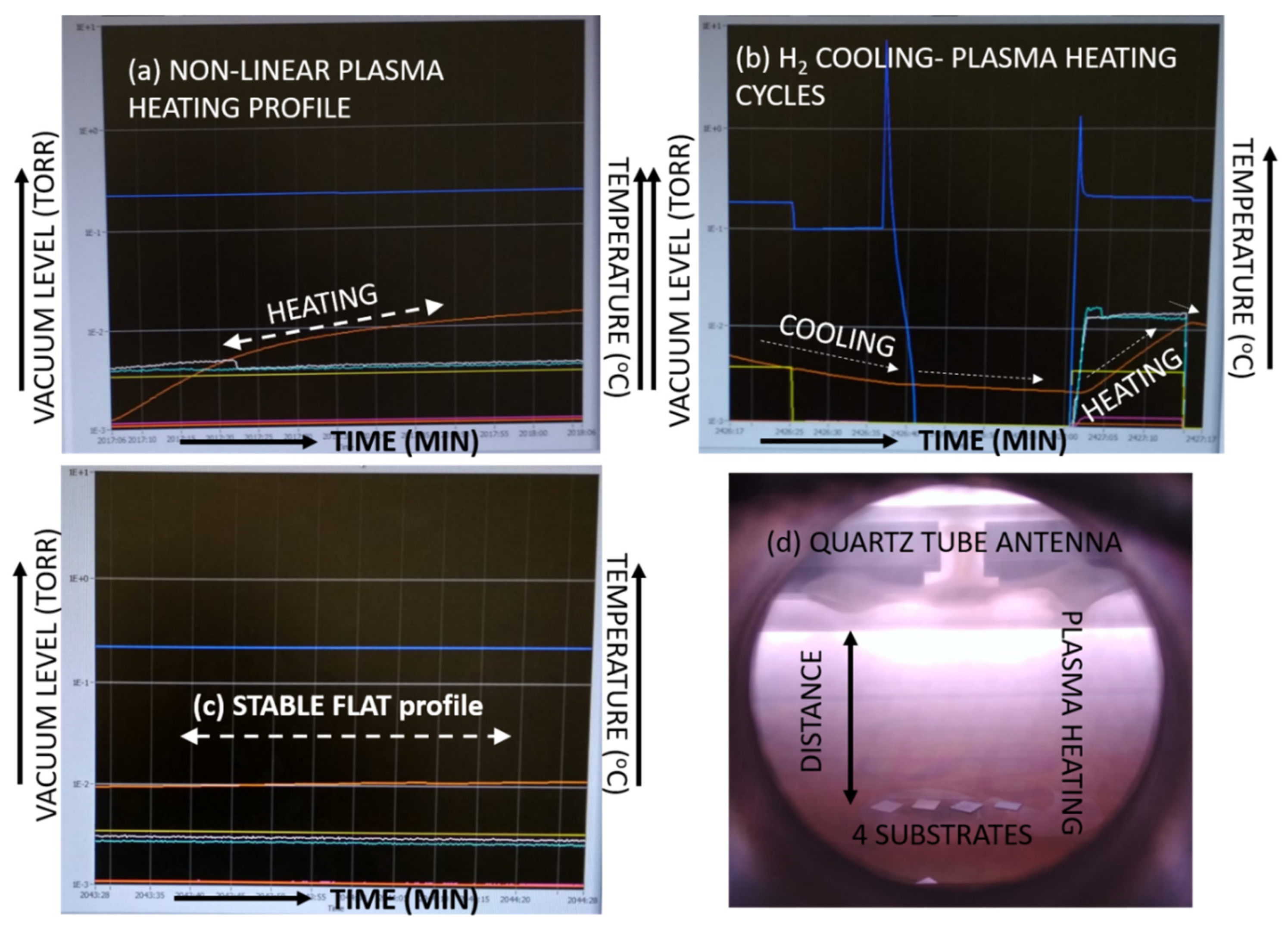
Figure 4.
Raman signals from the NCD crystals grown over DND seeded sapphire substrates after (a) 60, (b) 30 and (c) 15 minutes of LA-MPCVD growth at 1500 W power, 5 cm stage to antenna distance with gas recipe of H2:CH4:CO2=89:5:6.
Figure 4.
Raman signals from the NCD crystals grown over DND seeded sapphire substrates after (a) 60, (b) 30 and (c) 15 minutes of LA-MPCVD growth at 1500 W power, 5 cm stage to antenna distance with gas recipe of H2:CH4:CO2=89:5:6.
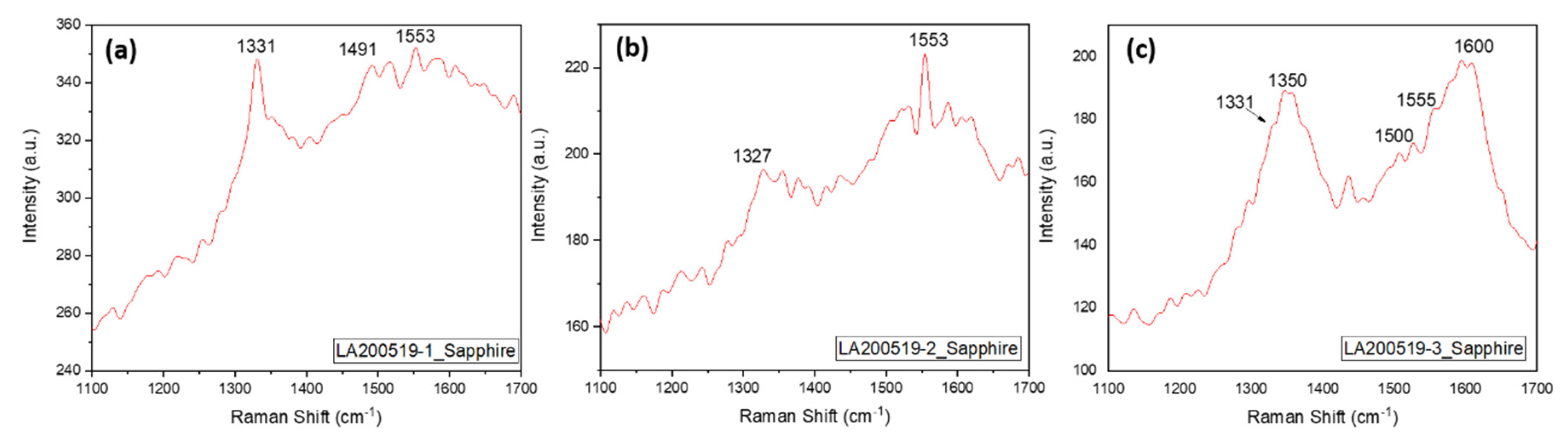
Figure 7.
SEM images of the NCD films (samples # LA200525-1) grown by pulse mode MW (input 300 W / output 2000 W) power on Si substrates at (a) 5 kX and (b) 50 kX magnifications; and on sapphire substrates at (a) 5 kX and (b) 50 kX magnifications.
Figure 7.
SEM images of the NCD films (samples # LA200525-1) grown by pulse mode MW (input 300 W / output 2000 W) power on Si substrates at (a) 5 kX and (b) 50 kX magnifications; and on sapphire substrates at (a) 5 kX and (b) 50 kX magnifications.
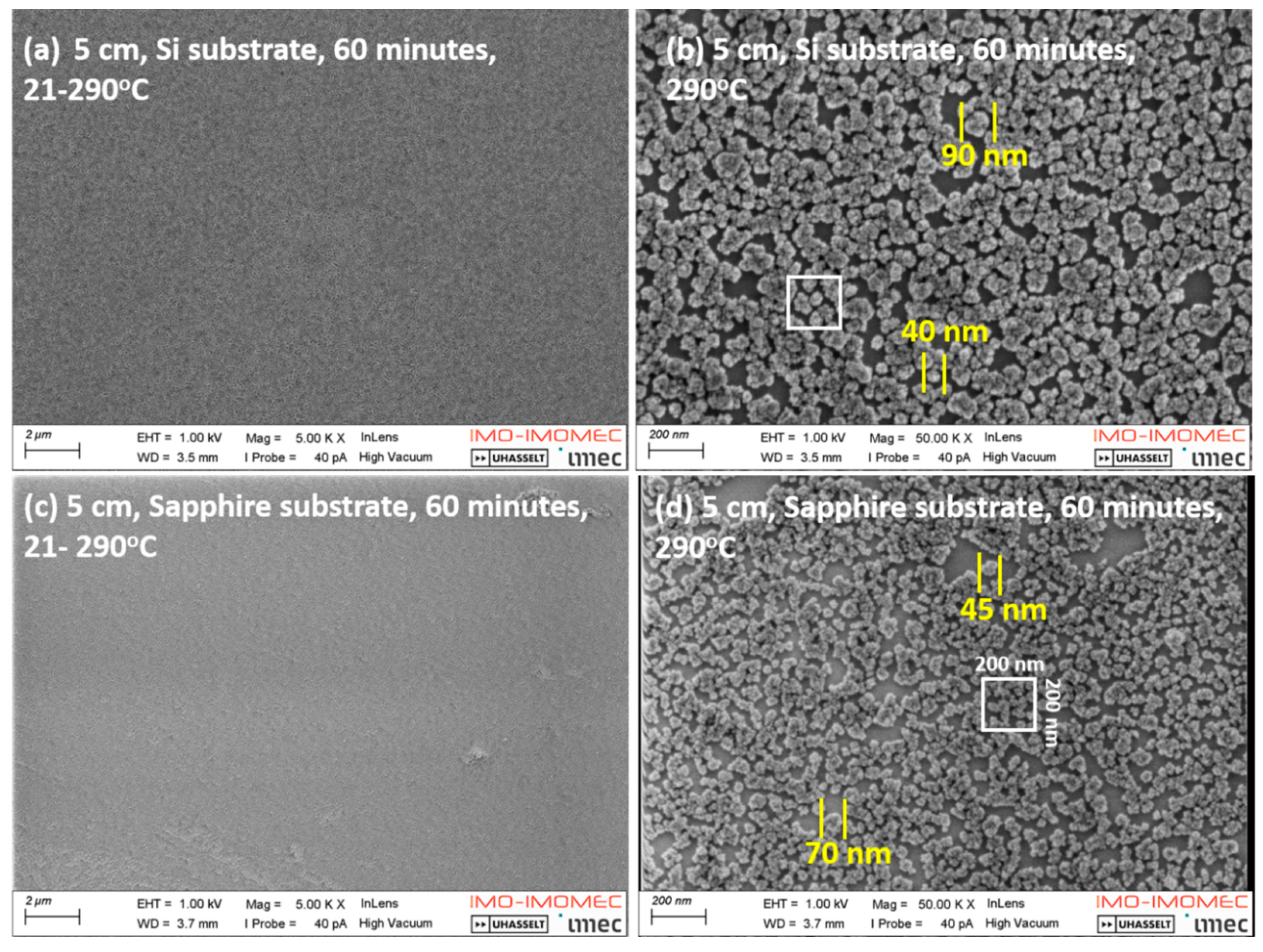
Figure 9.
Effect of LA-MPCVD plasma processing on EPD seeded substrates, without CO2 in the recipe, (a) Raman signal of the sample grown after 15 minutes, (b) Raman signal of the sample grown after 30 minutes, (c) top surface SEM at 20 kX magnification of the sample grown after 15 minutes and (d) top surface SEM at 20 kX magnification of the sample grown after 30 minutes, with 500X inset image showing survival of CNTs after plasma treatment.
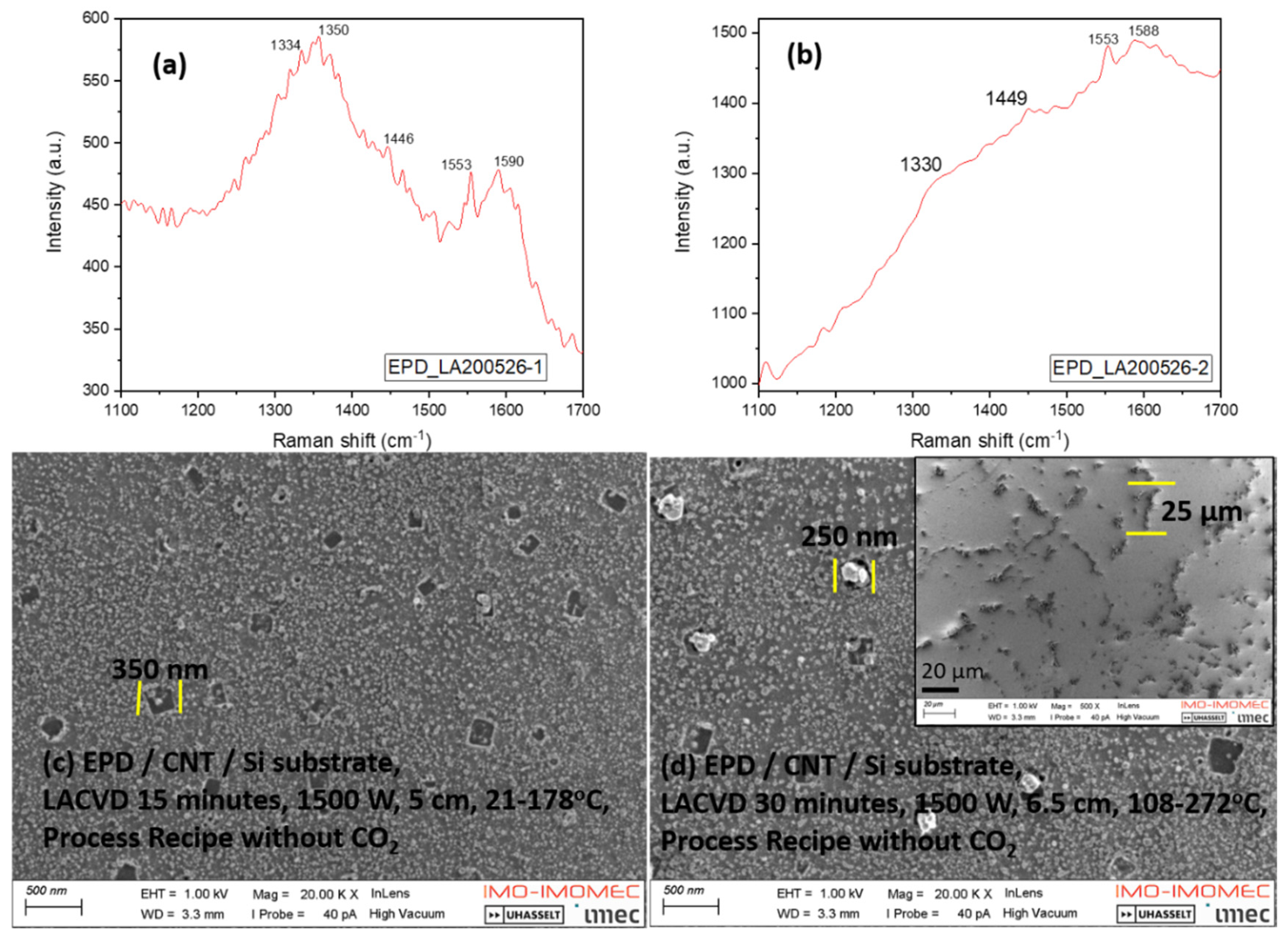
Figure 12.
SEM images of LACVD grown (1500 W, 5 cm) NCD crystals without CO2 gas in the recipe, after 15 minutes on DND seeded (a) silicon and (b) sapphire substrates; after 11 minutes on DND seeded (c) silicon and (d) sapphire substrates.
Figure 12.
SEM images of LACVD grown (1500 W, 5 cm) NCD crystals without CO2 gas in the recipe, after 15 minutes on DND seeded (a) silicon and (b) sapphire substrates; after 11 minutes on DND seeded (c) silicon and (d) sapphire substrates.
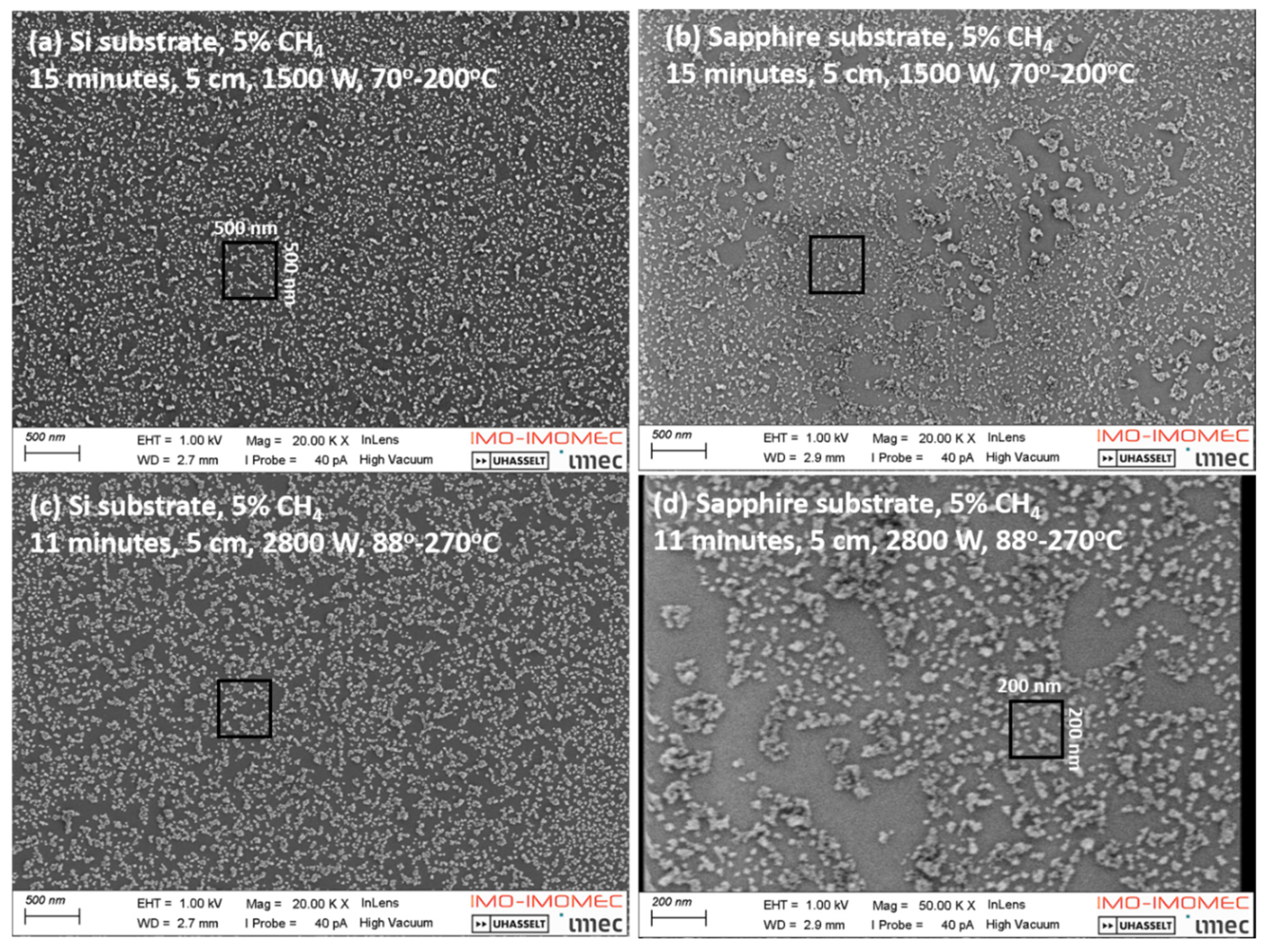
Figure 13.
SEM images of LA-MPCVD grown (1500 W) NCD crystals without CO2 gas in the recipe, grown after 15 minutes on DND seeded (a) silicon and (b) sapphire substrates at 5 cm stage to antenna distance; grown after 30 minutes on DND seeded (c) silicon and (d) sapphire substrates at 6.5 cm stage to antenna distance.
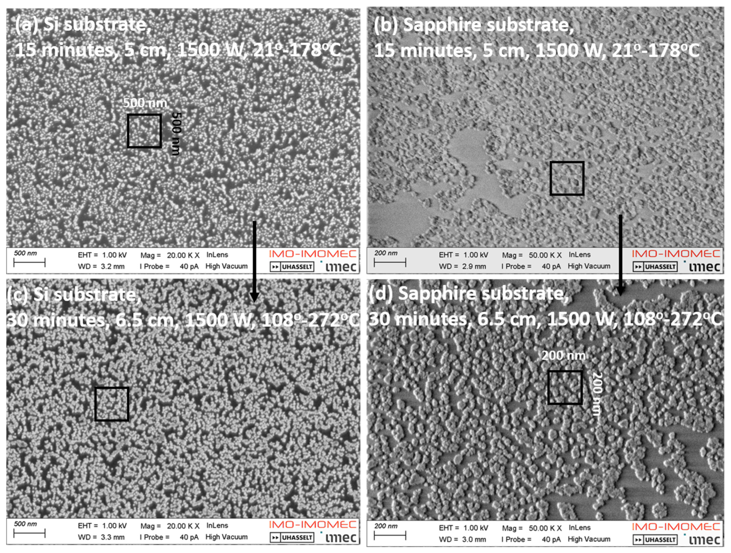

Table 1.
Process parameters of the samples deposited by LA-MPCVD.
| Sample # | Time (min.) | Substrate temperature (oC) | Heating rate (oC/min) |
NCD growth size (nm) | H2/CH4/CO2 (%) |
MW Power (W) | Pulse mode (frequency, duty cycle) |
Quartz tube to substrate distance (cm) |
|---|---|---|---|---|---|---|---|---|
| LA200519-1 | 60 | 21 - 284 | 4.4 | 140 (sapphire) | 89/5/6 |
1500 | NO | 5 |
| LA200519-2 | 30 | 108 - 272 | 5.5 | 30-70 (silicon) | ||||
| LA200519-3 | 15 | 111 - 236 | 8.3 | - | ||||
| LA200520-1 | 60 | 21 - 242 | 3.7 | 120 (sapphire) | 1100 | 5 | ||
| LA200520-2 | 120 | Stable 263 | - | 20-120 (sapphire) | 6.5 | |||
| LA200525-1 | 60 | 21 - 290 | 4.5 | 45-70 (sapphire) 40-90 (silicon) |
300 input / 2000 output | YES, 20 kHz, 45% |
5 | |
| LA200525-2 | 126 - 307 | 3 | 10-100 (silicon) | 6.5 | ||||
| LA200526-1 | 15 | 21 - 178 | 10.5 | 30 (silicon) 20-60 (sapphire) |
97/3/0 | 1500 |
NO |
5 |
| LA200526-2 | 30 | 108 - 272 | 5.5 | 45 (silicon) 25-100 (sapphire) |
6.5 | |||
| LA200605-1 | 15 | 21 - 170 | 9.9 | - | 96/4/0 | 5 | ||
| LA200605-2 | 70 - 200 | 8.6 | - | 95/5/0 | ||||
| LA200605-3 | 11 | 88 - 270 | 16.5 | - | 2800 |
Disclaimer/Publisher’s Note: The statements, opinions and data contained in all publications are solely those of the individual author(s) and contributor(s) and not of MDPI and/or the editor(s). MDPI and/or the editor(s) disclaim responsibility for any injury to people or property resulting from any ideas, methods, instructions or products referred to in the content. |
© 2023 by the authors. Licensee MDPI, Basel, Switzerland. This article is an open access article distributed under the terms and conditions of the Creative Commons Attribution (CC BY) license (http://creativecommons.org/licenses/by/4.0/).
Copyright: This open access article is published under a Creative Commons CC BY 4.0 license, which permit the free download, distribution, and reuse, provided that the author and preprint are cited in any reuse.
Submitted:
22 December 2023
Posted:
27 December 2023
You are already at the latest version
Alerts
A peer-reviewed article of this preprint also exists.
This version is not peer-reviewed
Submitted:
22 December 2023
Posted:
27 December 2023
You are already at the latest version
Alerts
Abstract
: Low-temperature growth of diamond films by chemical vapor deposition (CVD) method is not so widely reported and especially its initial periods of nucleation and growth phenomenon are of particular interest to the researchers. Four sets of substrates were selected for growing diamond films by linear antenna microwave plasma enhanced CVD (LA-MPCVD). Among them, silicon and sapphire substrates were pre-treated with detonation nanodiamond (DND) seeds before diamond growth for enhancement of its nucleation. On the other hand, carbon nanotube (CNT) films on Si substrates were also used as another template for LA-MPCVD diamond growth. In order to enhance the diamond nucleation during CVD growth, some of the CNT films were again pre-treated by electrophoretic deposition (EPD) of diamond nanoparticles. All these substrates were then put inside the LA-MPCVD chamber for growing diamond films under variable processing conditions. Microwave input powers (1100 – 2800 W), input power modes (pulse or continuous), antenna to stage distances (5 - 6.5 cm), process gas recipes (with or without CO2), methane gas percentages (3 - 5%), deposition times (11 – 120 minutes) were altered to investigate their effect on the growth of diamond film on the pre-treated substrates. The substrate temperatures were found to vary from as low as 170oC to a maximum of 307oC during the alteration of the different processing parameters. Contrary to the conventional MPCVD, it was observed that during the first hour of LA-MPCVD diamond growth, DND seeds or the nucleating structures, do not coalesce together to make a continuous film. Deposition time was the most critical factor in fully covering the substrate surfaces with diamond film, since the substrate temperature could not become stable during the first hour of LA-MPCVD. CNT was found to be oxidised rapidly under LA-MPCVD plasma conditions; therefore, a CO2-free process gas recipe was used to reduce CNT burning. Moreover, EPD-coated CNT was found to be less oxidised by the LACVD plasma during diamond growth.
Keywords:
Subject: Chemistry and Materials Science - Surfaces, Coatings and Films
1. Introduction
CVD growth of diamond films occurs within the temperature range of 700-1100oC [1]. There are also reports of growing diamond films at substrate temperatures of 500oC or less [2,3,4,5,6]. Linear antenna microwave plasma enhanced CVD (LA-MPCVD) is a process [7,8,9,10,11,12,13] that allows growing diamond crystals at lower substrate temperatures [14,15,16]. However, there is very little literature available where growth has been reported at less than 300oC temperature [17,18]. Reporting of the respective substrate temperature during CVD has mostly been done in situ, by optical pyrometers [19], but low LA-MPCVD processing temperatures do not allow to use of such optical instruments [15]. Therefore, thermocouples and infrared thermometers are placed underneath the substrate stage to record reliably the LA-MPCVD growth temperatures, where it is protected or uninfluenced from the effect of CVD plasma in the diamond growth environment. In this paper, experiments have been designed to allow diamond growth at less than 300oC. It is also well known that during the first few minutes of CVD deposition, diamond film coalesces together to cover the entire pre-seeded substrate surface [20]. Due to the very slow growth rates (5-50 nm/hr) during the LA-MPCVD process, all the above cited articles have been reported to grow continuous nanocrystalline diamond (NCD) films over long (8-20 hrs) deposition periods. But there is little or no information about diamond growth behaviour during the first hour of LA-MPCVD processing. Neither there is any data over the time period which should be allowed to effectively cover the substrate surface under LA-MPCVD processing conditions [21,22]. The primary obstacle in chemically synthesising diamond is the fact that the starting point should be diamond itself as seed particles. Without appropriate nucleating agent, diamond growth incubation time can be very long, and researchers have tried many methods for the nucleation enhancement during CVD growth of diamond [23,24,25,26,27]. Mechanical or ultrasonic scratching of the substrates with abrasives [28,29] and detonation nanodiamond (DND) seeding [30,31] are the most commonly used techniques for promoting nucleation of diamond films before starting the CVD process. However, there are very few reports of nucleation enhancement by electrophoretic deposition (EPD) [32,33,34,35]. Here it has been attempted for the first time, both the EPD and DND seeding techniques for nucleation enhancement on different substrates.
Potocky et al. [36,37] also investigated the growth of carbon nanotubes (CNT) using linear antenna CVD system with RF biasing of the substrate for 10 min and 40 min durations. Another paper from the same research group [18] reported LA-MPCVD plasma treatment of polymer passivated NCD layers for enhancement of the diamond surface conductivity by surface hydrogenation. Their research showed that 200oC is the optimum substrate temperature to effectively hydrogenate the NCD surface and simultaneously without damaging the metallic contacts or the top polymeric resist layer used for electronics. Potocky et al. [36] concluded that CNTs grown by LA-MPCVD are hydrophobic with contact angle greater than 130o. They used oxygen plasma treatment of 5 min. for enhancing the CNT surface wettability. But they did not attempt to grow diamond films on top of their CNTs [38], which has so far been attempted by the researchers with limited success. It has been reported that CNT covered with NCD are better field effect transmitters [39,40]. In the present work, CNT was grown separately by a thermal CVD reactor on Si substrates, before performing LA-MPCVD of the diamond films onto them. But being hydrophobic, CNT could not be seeded (essential for growing diamond by CVD) with water based DND solution, as could be done for other regular hydrophilic silicon or sapphire substrates. Therefore, EPD was used for seeding the CNT/Si substrate with nanodiamonds for further diamond growth by LA-MPCVD. Such diamond coated CNTs will have applications in electron field emission.
2. Materials and methods
2.1. Substrates
Silicon and sapphire substrates, laser cut into 10×10 mm2 sizes, were used for CVD diamond growth. Silicon substrates were cut out from commercially available p-type 0.5 mm thick 4-inch wafers with a resistivity of 20 ohm-cm. Sapphire substrates were single crystal wafers from the commercial supplier Kyocera. Both of them were seeded with nanodiamonds to enhance the diamond nucleation during CVD growth as described in section 2.1.1.
2.1.1. DND seeding
Water-based detonation nanodiamond (DND) slurry was spin-coated on top of the silicon and sapphire substrates with a rotating speed at 4000 rpm by a spin coater (Laurell Technologies Corporation, model WS-400B-6NPP/LITE) for 40 sec, along with brief rinsing with distilled water, until the surfaces become completely dry [41]. Such monolayer-seeded substrates were then loaded into the LA-MPCVD chamber. Figure 1a is the SEM image of the DND-seeded silicon substrate. The nucleation density was calculated to be 2×10¹⁰/cm2. Figure 1b is the x-ray diffraction of the sapphire substrate used in this study.
2.1.2. CNT and EPD
Other than the conventional DND seeding procedure, two separate sets of silicon substrates were also prepared. One set of substrates was carbon nanotubes (CNT) deposited on silicon wafers by iron catalyst-assisted thermal CVD. The other set was prepared by further electrophoretically depositing diamond on top of such CNT/Si substrates.
The growth conditions of CNTs were a working pressure of 3 Torr, a growth time of 20 min at 750℃ with gas flow rates of NH3 and C2H2 of 10 sccm and 40 sccm, respectively. Figure 1c shows the SEM image of the top surface of the CNT/Si substrate. The length of CNTs was found to be 510 µm (inset).
In order to protect the CNTs from plasma damage during deposition of the diamond film, the diamond nanoparticles were coated on top of the CNTs by electrophoretic deposition (EPD). In the EPD process, water based nanodiamond solution (Nanoseed 18 by Micro Diamant AG Switzerland) was used. The earlier prepared CNTs/Si substrates were biased at about +20 V with respect to the reference electrode, the Pt, for 20 s. Figure 1d shows the SEM photograph of the diamond nanoparticles on top of the CNT/Si substrate. The nucleation density was estimated at about 4.7×10¹⁰/cm2.
Figure 1.
(a) SEM image of the DND seeded silicon substrate, (b) XRD of sapphire substrate, (c) CNT coated silicon substrate, inset SEM showing cross-sectional CNT length and (d) top view of the EPD of diamond nanoparticles on the CNT/Si substrate.
Figure 1.
(a) SEM image of the DND seeded silicon substrate, (b) XRD of sapphire substrate, (c) CNT coated silicon substrate, inset SEM showing cross-sectional CNT length and (d) top view of the EPD of diamond nanoparticles on the CNT/Si substrate.
2.2. LA-MPCVD
All the four set of substrates were loaded together inside the linear antenna microwave plasma-enhanced CVD chamber. No heater was used for additional heating of the substrates. Total volume of the process gases was fixed at 150 sccm and therefore, the working pressure was also fixed at 0.23 mbar. The base pressure achieved before starting the deposition run was in the order of 10-4 Torr. The experimental conditions are described in the following Table 1.
Deposition periods were varied from 11-120 minutes. The substrates were solely heated by the microwave plasma, therefore, depending on the individual CVD period, the substrate stage temperatures were different, as described in the Table 1. For example, samples # LA200519-1 were loaded at room temperature of 21oC inside the LA-MPCVD chamber and after achieving the base pressure of 7×10⁻⁴ Torr, the plasma was ignited with the introduction of the processing gases. 1500 W of average power was achieved by switching on two 2.45 GHz magnetrons. The deposition was carried out for 60 minutes and the final temperature recorded was 284oC. It is to be noted that the substrate stage temperature continues to rise during the whole deposition period and the LA-MPCVD plasma heating profiles are depicted in Figure 2. After the each CVD run was over, the plasma was put off by disconnecting power supplies to the magnetrons and only the hydrogen gas was allowed to flow through, in order to cool down the substrate stage below 140 oC (permissible temperature safety limit of the reactor), before unloading and loading the next set of 4-substrates. An example of LA-MPCVD cycle of cooling with hydrogen gas flow, thereafter plasma heating (11-minute-long for samples # LA200605-3) and again successive cooling profile is shown in Figure 2b. However, if the deposition time is long enough like that for the samples # LA200520-2, the temperature profile looks very much stable and flat at 263oC towards the end of the LA-MPCVD run, as shown in Figure 2c. Table 1 describes widely variable heating rates because the non-linear nature of the respective heating profiles by the plasma. During the initial LA-MPCVD periods, the temperature rise was steeper, which thereafter slows down to a flatter curve (Figure 2a), before achieving a flat stable temperature regime (Figure 2c). Figure 2d describes the plasma heating of the four samples together during the LA-MPCVD D run. The processing was either with CO2 or without CO2 gas in the precursor recipe as shown in the Table 1. The reactor chamber was intermittently plasma cleaned by flowing 200 sccm oxygen at 2800 W average input microwave power, for a time duration, matching with the previously concluded CVD run period. The minimum duration of CVD run was 11 minutes, whereas, the maximum CVD time was 2 hr long in the current set of experiments. The distances were 5 and 6.5 cm between the substrate stage and the linear antenna quartz tube, as determined by trial and errors, for optimum NCD film generation. The microwave input power was mostly in continuous wave (CW) mode, except for one set of experiments (samples # LA200525), in which pulsed mode input microwave power was applied at 20 kHz frequency and 45% duty cycle.
2.3. Physical characterisations
The samples were examined by scanning electron microscope (SEM- FEI Quanta 200 FEG) for evaluating the efficacies of different processing conditions of the CVD diamond growth. Raman spectroscopy (HORIBA Jobin Yvon T64000 spectrometer using laser light of 488 nm wavelength) was also used to confirm the presence of nanodiamond film. X-ray diffraction (XRD) was used to get the characteristic substrate peaks for sapphire.
3. Results and discussion
In this work, silicon and sapphire substrates have been seeded following standard DND monolayer dispersion technique [41] before growing diamond by LA-MPCVD [15]. Another set of substrates with CNT on silicon were also prepared for LA-MPCVD diamond growth of diamond. Conventional water based DND suspension could not be used for seeding the CNT/Si substrates since the as-grown CNT was hydrophobic. Therefore, EPD was used to seed the CNT/Si substrate for nucleation enhancement, reported here for the first time, before LA-MPCVD growth. It is expected that EPD treated diamond will be better template for diamond growth than untreated CNT/Si substrate for growing diamond inside the LA-MPCVD reactor.
3.1. First hour of LA-MPCVD growth
3.1.1. Silicon substrates
Figure 3 compares the NCD growth patterns after 15, 30 and 60 minutes of LA-MPCVD runs. Figure 3a, Figure 3b and Figure 3d show gradual increase in the size of the diamond nanocrystals with increasing deposition time. After the first 15 minutes of LA-MPCVD, the nanodiamond seed crystals, which are typically 4-6 nm in sizes or their agglomerates (Figure 1a), grew into bigger sizes but did not become large enough to effectively touch each other in order to form connecting network of diamond nanocrystals (Figure 3a – the current SEM image magnification was not high enough to determine the respective NCD sizes after 15 minutes of LA-MPCVD growth). As the deposition time is increased to 30 minutes and further into 60 minutes of LA-MPCVD, the diamond nanocrystals start touching each other but still not enough to completely cover the underlying silicon substrate. The black contrasting substrate features are gradually found to diminish in the corresponding SEM images (Figure 3a, Figure 3b and Figure 3d, respectively). It was easier to calculate the uncovered substrate surface areas than the size of the individual NCDs grown over them after 15 minutes of LA-MPCVD. The average lengths of the uncovered silicon substrate areas were more than 270 nm (Figure 3a) after 15 minutes of LA-MPCVD run, and were reduced but not enough to let the nanodiamond crystals touch each other after 30 minutes of LA-MPCVD, as shown in Figure 3e. The sizes of the nanodiamond seed crystals is found to grow to about 30 nm isolated nanocrystals or to their agglomerates of 60-70 nm sizes in Figure 3e. Even after 60 minutes of LA-MPCVD, 150-200 nm long uncovered silicon areas were still visible in Figure 3d. It is important to notice that the 30 nm or 70 nm NCDs, shown in Figure 3e are actually agglomerations of tinier (about 10 nm) nanoparticles.
The Raman spectra from the diamond nanocrystals after 15 minutes of LA-MPCVD is found to be very noisy (Figure 3f) with a small sp3 peak at 1335 cm-1 in contrast to disordered graphite (D) band at 1351 cm-1. There are also Raman peaks at 1448, 1553 and 1582 cm-1, which correspond to trans-poly-acetylene (TPA) and graphite crystals (G) respectively in the growing NCD film. On the other hand, the sp3 Raman signal after 60 minutes of LA-MPCVD diamond growth is found to be very strong (Isp3= 156) with FWHM of 18 cm-1 (Figure 3c). The corresponding non-diamond Raman peaks for TPA (1140 and 1480 cm-1) and G-band (1553 cm-1 and hump thereafter) are also present but at much-reduced level (Isp2=60), indicating growth of good quality diamond nanocrystals. The sp3 Raman peak signal enhancement in Figure 3c in comparison to Figure 3f is due to the combined effect of increased LA-MPCVD deposition time, which also helped to achieve higher substrate temperatures. It is important to note that the NCD growth temperature is dynamic and continuously increasing by the deposition time over which the stage was allowed to be heated by the microwave plasma. The longer the CVD time period, the higher the substrate temperature - until the substrate temperature becomes gradually stable with the progressing time. 15-60 minutes of heating by the plasma does not allow the substrate temperature to become stabilised (Figure 2a).
Figure 3.
NCD crystals on DND seeded silicon substrates, (a) SEM of the sample grown after first 15 minutes, (b) SEM of the sample grown after 30 minutes at 20kX magnification, (c) Raman spectra of the sample grown after 60 minutes, (d) SEM of the sample grown after 60 minutes, (e) SEM of the sample grown after 30 minutes at 200kX magnification and (f) Raman spectra after of the sample grown 15 minutes of LA-MPCVD growth.
Figure 3.
NCD crystals on DND seeded silicon substrates, (a) SEM of the sample grown after first 15 minutes, (b) SEM of the sample grown after 30 minutes at 20kX magnification, (c) Raman spectra of the sample grown after 60 minutes, (d) SEM of the sample grown after 60 minutes, (e) SEM of the sample grown after 30 minutes at 200kX magnification and (f) Raman spectra after of the sample grown 15 minutes of LA-MPCVD growth.
3.1.2. Sapphire substrates
Figure 4 shows the corresponding Raman spectra from the NCDs grown over DND-seeded sapphire substrates, kept alongside the silicon substrates as shown in Figure 2d. Here it is also found that the sp3 Raman peak in and around 1331 cm-1 is the sharpest with a FWHM of 15 cm-1 (Figure 4a), from the NCD grown over the longer time period of 60 minutes. In fact, NCDs grown over sapphire substrate have better FWHM values than NCDs grown over silicon substrates (Figure 3c). The sp3 Raman signals become gradually weaker (figures 4b and 4c) and other non-diamond peaks (TPA - 1491, graphitic D - 1350 and G – 1600 cm-1) become stronger due to the presence of smaller NCDs, with the reduction in LACVD time periods.
3.1.3. CNT and EPD substrates
The SEM and Raman spectroscopy results from the CNT/Si and EPD-diamond/CNT/Si substrates kept alongside the silicon and sapphire DND seeded substrates are shown in Figure 5, after 15 minutes of LA-MPCVD processing. Longer CVD growth periods of 30 and 60 minutes, were completely etching the CNTs due to the oxidation by the microwave plasma recipe of H2:CH4:CO2=89:5:6. The well connected CNT network shown in Figure 1c is found to be etched completely by the LA-MPCVD plasma even after 15 minutes into the deposition period, as shown in figures 5a and 5d. However, the EPD treated CNT/Si substrate is found to be less affected by the LA-MPCVD plasma, as the length of individual CNTs are found to be longer (>20 µm) in Figure 5a than that in Figure 5d (<5 µm). Figure 5b is the higher magnification image of Figure 5a, taken from the intermediate region of the individual CNTs. It shows that the substrate surface is fully covered with carbonaceous film. The Raman signal of such film is shown in Figure 5c with stronger sp3 signal at 1335 cm-1 along with another less intense peak at 1559 cm-1 for graphitic carbon. The image 5b consists of tiny individual NCD grains (20-60 nm) present all over the EPD-diamond/CNT/Si plasma treated surface along with square shaped holes (140-280 nm). Such rectangular or square holes are also present on the CNT/Si plasma treated surface (Figure 5e) but much smaller in sizes (50-100 nm). Correspondingly, the individual diamond nanoparticles that are present all over the substrate surface in Figure 5e, are also smaller in sizes (20-40 nm) than those found in Figure 5b. Similarly, the sp3 (1334 cm-1) and graphitic (1588 cm-1) carbon signals from the plasma treated CNT/Si surface (Figure 5f) are also weaker, along with the presence of peaks at 1453 cm-1 which is due to TPA. The presence of sp3 Raman signal from the LA-MPCVD plasma treated CNT/Si substrates confirms the fact that even without nanodiamond seeding it was possible to deposit NCD on top of CNTs.
There are few white particles that are found to be present inside the rectangular holes (Figure 5b and Figure 5e). The holes might have been created with the dislodgment of such white particles. Thus, it is found that the EPD treated CNTs are burnt to a less extent by the LA-MPCVD plasma (comparing Figure 5a and Figure 5b). Moreover, it is also possible to grow CVD diamond onto CNT/Si substrate without the need of nanodiamond seeding (Figure 5f).
Figure 5.
EPD-diamond /CNT/Si substrate after 15 minutes of LA-MPCVD plasma treatment, (a) SEM at 500X magnification, (b) 20kX magnification, (c) Raman signal. EPD-diamond CNT/Si substrate after 15 minutes of LA-MPCVD plasma treatment, (d) SEM at 500X magnification, (e) 20kX magnification, (f) Raman signal. CNT/Si substrate after 15 minutes of LA-MPCVD plasma treatment.
Figure 5.
EPD-diamond /CNT/Si substrate after 15 minutes of LA-MPCVD plasma treatment, (a) SEM at 500X magnification, (b) 20kX magnification, (c) Raman signal. EPD-diamond CNT/Si substrate after 15 minutes of LA-MPCVD plasma treatment, (d) SEM at 500X magnification, (e) 20kX magnification, (f) Raman signal. CNT/Si substrate after 15 minutes of LA-MPCVD plasma treatment.
3.2. Low MW power
The substrate temperatures that can be achieved inside the LA-MPCVD reactor, solely by means of plasma heating, depends on the input MW power and also on the stage to antenna distances. Therefore, in the next set of experiments, the MW power was reduced to 1100 W and also the stage to antenna distances were varied from 5 to 6.5 cm in order to see its effect on the growth of nanodiamond crystals during the early periods of LA-MPCVD. The lowest possible substrate temperature (15 hours of deposition) that Izak et al. [14] could achieve was 250oC by lowering the input microwave power to 1200 W. They also used 1700 W and 2500 W of higher input MW powers. However, they did not mention the substrate to antenna distance used in their experiments. Reportedly [11,16,22] it is kept at 5-7 cm optimal distances to achieve 400-450oC stable substrate temperature by plasma heating. Closer distances like 4 cm could produce 550oC substrate temperatures. In order to achieve higher substrate temperatures (>600oC), it is usually done by resistive heater underneath the substrate.
The substrate temperature continues to rise from the room temperature to 242oC, until the end of one-hour long LA-MPCVD run (Table 1, samples # LA200520-1). Surprisingly, at the lower MW of 1100 W, the NCDs were found to almost cover the entire silicon substrate (Figure 6a), which was not observed even at 1500 W (Figure 3d). Higher magnification SEM image in Figure 6b, reveals the NCD sizes to be around 40-100 nm. Still there are intermediate bare substrate areas visible in between the NCD grains. There is no evidence of secondary nucleation. The NCD seems to grow in lateral direction in order to cover the substrate surface by a single layer coalescing film.
Figure 6c (sapphire sample # LA200519-1) and Figure 6d (sapphire sample # LA200520-1) compare the effect of lowering the input MW power on the diamond growth behaviour during the first 60 minutes of LA-MPCVD processing with identical stage to antenna distance of 5 cm. 1500 W input MW power seems only to heat the substrate to a higher temperatures of 284oC, starting from room temperatures, but higher power did not help in effective grain coalescence - as it seems to be possible with 1100 W power as shown in Figure 6d. The sizes of the NCDs are comparable in between Figure 6c (approximately 140 nm NCDs scattered and isolated from each other) and 6d (about 120 nm NCD agglomerates). However, at lower power the grains are more coalesced and interconnected (Figure 6d). It appears that lower input power is beneficial to lateral growth of the diamond nanocrystals. There is still no sign of secondary-nucleation.
Figure 6.
Nearly coalesced NCD crystals grown by LA-MPCVD reactor at reduced power level of 1100 W on silicon substrate for 60 minutes, (a) 20kX and (b) 50kX magnification SEM images. Comparison of diamond nanocrystals coalescence on sapphire substrates after 60 minutes of LA-MPCVD at MW power levels of (c) isolated, at 1500 W and (d) connected, at 1100 W.
Figure 6.
Nearly coalesced NCD crystals grown by LA-MPCVD reactor at reduced power level of 1100 W on silicon substrate for 60 minutes, (a) 20kX and (b) 50kX magnification SEM images. Comparison of diamond nanocrystals coalescence on sapphire substrates after 60 minutes of LA-MPCVD at MW power levels of (c) isolated, at 1500 W and (d) connected, at 1100 W.
3.3. Pulse mode MW power
Pulse mode operation of LA-MPCVD reactor helps in achieving better quality diamond crystals with further reduction in input power level [13]. When the input MW power was 300 W, at 20 kHz pulse frequency and 45% duty cycles, the average output MW power recorded was 2000 W (Table 1). During the first hour LA-MPCVD run for the samples # LA200525-1, the substrate temperature continues to rise from room temperature to 290oC (similar to 1500 W, samples # LA200519-1) at a stage to antenna distance of 5 cm, however, after stopping the first run at the end of 60 minutes, the substrate was let to cool down to 140oC (reactor component safety temperature limit before opening the chamber door) before loading the second set of samples (# LA200525-2). Therefore, the starting temperature for the second run (# LA200525-2) was 126oC – it was not the room temperature, like it was for the previous first run (# LA200525-1). LA-MPCVD starting temperature of 126oC enables the substrate temperature to attain even higher value of 307oC after 60 minutes of plasma heating, even at a longer stage to antenna distance of 6.5 cm.
Figure 7 are the lower (5 kX - 7a and 7c) and higher magnification (50 kX - 7b and 7d) images of the silicon and sapphire substrates from the LA-MPCVD run # LA200525-1. It is found that pulse mode helped in producing denser film coverage of the silicon substrate (figures 7a and 7b) surfaces in comparison to 1500 W (# LA200519-1, Figure 3d) continuous mode input MW power runs after 1 hour of LA-MPCVD. However, if the figures 7a and 7c are compared, it appears that the sapphire substrates are more successfully covered (less contrasting black substrate areas) with diamond nanocrystals. But their respective higher magnification images reveal that the size of nanodiamonds are somewhat bigger (40-90 nm) on silicon substrates than that on the sapphire substrates (45-70 nm), and the respective grain size distribution is also narrower. The NCD sizes may be bigger for silicon substrates but their densities (≈7 NCDs on silicon against ≈12 NCDs on sapphire over 200 nm×200 nm substrate areas) are higher for the sapphire substrates – indicating favourable growth on the sapphire substrates. But still, the pulse mode could not produce continuous NCD films on both the substrates. The primary reason is the unstable (continuously rising, 21o – 290oC) substrate temperature, which did not allow to grow nanodiamond crystals, fully covering the substrate surface.
3.4. Fully coalesced NCD films
It was found, that, even after 60 minutes of LA-MPCVD processing, at higher power of 1500 W, or lower power of 1100 W, or even with pulse mode MW power, at a stage to antenna distance of 5 cm, none of the processing conditions, could produce continuous diamond films on both the DND seeded silicon and sapphire substrates. Had this been conventional resonant cavity microwave plasma CVD reactor, it would have produced continuous micron thick high quality NCD films with H2/CH4/CO2 = 89/5/6 process recipe after 1 hour of growth [1]. Next, it was attempted to lower the substrate stage to 6.5 cm distance away from the linear antenna quartz tube, in order to lower the substrate temperature. In effect, it was as to promote less etching of the deposited films nearer to the antenna, and producing a continuous film formation on the substrate surface - even if it will be poorer in diamond quality.
Lowering the stage from 5 cm to 6.5 cm is beneficial to the substrate surface. Figure 8a and its inset which were the diamond film SEM images on silicon substrate after 1 hr LA-MPCVD in pulse mode at 5 cm distance, still show dark contrasting uncovered silicon substrate areas underneath, but the nanodiamond grains are more or less connected with each other without any sign of isolated NCDs. It appears from the Figure 8a that the pulse mode was more effective processing condition in covering the substrate surface with single layer of NCD film. But if the distance is increased to 6.5 cm (Figure 8b and inset), there is sign of secondary nucleation which may produce poor quality diamond. It concludes that wider stage to antenna distance helped in secondary nucleation to take place and produced almost fully covered silicon substrate. The Raman signal from such semi-continuous NCD film on sapphire substrate shows very high FWHM of 40 cm-1 for the sp3 peak at 1333 cm-1, along with appearance of TPA peak at 1502 and graphite G peaks at 1606 and 1552 cm-1. The high value of FWHM confirms the presence of secondary nuclei, as evident also from the SEM image. The end temperature of the second 60-minute LA-MPCVD run was somewhat higher at 307oC, as its starting temperature was also higher at 126oC - after the end of first experiment of 60 minutes LA-MPCVD which started from room temperature of 21oC. But both of them were not performed long enough to make the substrate temperature reaching a stable flat curve. The substrate temperature was continuously changing (increasing) during both the runs – initially at a faster pace (steep slope) and later on at slower (flatter slope) heating rates.
It was found that for the samples # LA200520-2, grown at longer substrate to antenna distance of 6.5 cm, and grown for longer duration of 2 hrs, LA-MPCVD process conditions could produce a flat substrate temperature curve as shown in Figure 2c. The longer distance of 6.5 cm promoted in producing secondary nucleation of diamond crystals (wide range of NCD grain sizes from 20-120nm – Figure 8f) and longer time of LA-MPCVD allowed the films to coalesce to form full substrate coverage as shown in figures 8d-f. Earlier it was also found that lower power of 1100 W contributed to produce better film coverage (Figure 6a) than 1500 W on silicon substrate (Figure 3a). Figure 6d is the NCD film after 1 hr LA-MPCVD on sapphire, showing underlying bare substrate but if the LA-MPCVD was allowed to proceed for another 1 hr, it was found to fully cover the sapphire substrate surface (Figure 8e and Figure 8f). Figure 6d shows a cluster of 12 diamond nanoparticles, with 120 nm total diameter. Although every grain is not of equal dimension, but it may be estimated that the individual nanodiamond crystals are 5-10 nm in size. This was the case after 1 hr of LA-MPCVD on sapphire substrate, but when the LA-MPCVD was proceeded for another 60 minutes, it is found to produce secondary nucleation with variable nanodiamond sizes of 120, 60 or 30 nm of individual grain sizes (Figure 8f). Therefore, longer periods of LA-MPCVD helped to grow the film both laterally and in three dimensions due to secondary nucleation. Researchers have earlier reported [22] that there are high pressure growth regime which promotes diamond re-nucleation and low pressure growth regime which promotes lateral growth. Low electron temperature inside LA-MPCVD is essential for continuous re-nucleation of diamond in hydrogen rich plasma [42].
Figure 8.
Coalescence and secondary nucleation of NCDs. SEM of (a) interconnected NCD on Si, pulse mode at 5 cm, (b) secondary nucleated NCDs on Si in pulse mode at 6.5 cm, (c) Raman spectra from secondary nucleated NCD after 1 hr LA-MPCVD in pulse mode at 6.5 cm. SEM images of NCDs after 2 hr LA-MPCVD in CW mode at 6.5 cm, 1100 W power (d) on Si, (e) sapphire substrates and (f) 50 kX magnification of image in 8e.
Figure 8.
Coalescence and secondary nucleation of NCDs. SEM of (a) interconnected NCD on Si, pulse mode at 5 cm, (b) secondary nucleated NCDs on Si in pulse mode at 6.5 cm, (c) Raman spectra from secondary nucleated NCD after 1 hr LA-MPCVD in pulse mode at 6.5 cm. SEM images of NCDs after 2 hr LA-MPCVD in CW mode at 6.5 cm, 1100 W power (d) on Si, (e) sapphire substrates and (f) 50 kX magnification of image in 8e.
3.5. LA-MPCVD growth without CO2
3.5.1. EPD-diamond/CNT/Si substrates
It was found that the EPD treated CNT/Si substrates were also etching out fast under the LA-MPCVD plasma recipe of H2:CH4:CO2=89:5:6. Therefore, in order to reduce the effect of oxidation, in the next set of experiments, CO2 gas was removed from the process recipe. Figure 9a and 9b show the Raman spectra of the EPD seeded CNT/Si substrates after 15 and 30 minutes of LA-MPCVD plasma treatment without CO2 in the recipe of H2:CH4=97:3. It was found that even after 30 minutes of LA-MPCVD, CNT survived the plasma conditions (inset Figure 9d). The corresponding Raman signal of the sp3 peak was weaker than those of the graphitic D-band (Figure 9a) after 15 minutes of LA-MPCVD, however, the Raman spectra started producing fluorescent signals after 30 minutes of LA-MPCVD as shown in Figure 9b. There lies a definitive signal (not prominent enough due to background fluorescence) for diamond at 1330 cm-1 which was taken from the sample in Figure 9d. There are loosely scattered diamond nanoparticles, of around 80 nm diameter or less, all throughout the images in 9c and 9d. There is some occasional appearance of square or rectangular holes in the plasma treated EPD-diamond/CNT/Si substrate surface. Sizes of those holes vary from 250-350 nm. It is interesting to see that some of the holes were occupied by bright whitish nanoparticles - its dimensions was measured to be 250 nm. It can be assumed that dislodgment of such white particles resulted in the creation of those square or rectangular holes. The SEM images of figures 9c and 9d were taken from the intermediate regions of the individual CNTs (inset image of Figure 9d). The sizes of the some of the CNTs are found to be as big as 25 µm. If the CNT lengths in Figure 9d are compared with those in figures 5a (20 µm after15 minutes LA-MPCVD), it is concluded that even after 30 minutes of LA-MPCVD plasma treatment, EPD seeded CNT/Si survived diamond deposition conditions without complete etching, due to the absence of CO2 in the recipe.
3.5.2. Silicon and sapphire substrates
3.5.2. a. Effect of CH4
Section 3.1.1. and Section 3.1.2. have already shown that the early periods of low temperature LA-MPCVD run could not produce fully covered, otherwise perfectly DND seeded silicon and sapphire substrates (even after 60 minutes of deposition). One of the reasons of the slow growth of diamond crystals, could have been rapid etching of the nanodiamond films by the CO2 present in the plasma recipe. Therefore, it was further investigated to see the effect of removing CO2 from the recipe during the LA-MPCVD nanodiamond growth. Researchers [43] have shown that at the low CO2 concentration (less than 0.5%), there is formation of SiC in competition with the growth of boron doped NCD during the LA-MPCVD process, which is due to the silicon contamination from the quartz tube. Moreover CO2 (less than 1%) enhances the NCD growth rate (16 nm/hr) in continuous mode LA-MPCVD. But an increase in CO2 gas over CH4 gas percentages reduced [11,13] the growth rate (7 nm/hr). But there is no report so far about the effect of CH4 percentages on the NCD growth pattern, specifically during the unstable periods of LA-MPCVD run, i.e., until the stable substrate temperature is achieved.
Figure 10a, Figure 10b and Figure 10c are the SEM images of the NCD crystals grown over the Si substrates with the increasing methane percentages (3% - 5%), only after first 15 minutes of LA-MPCVD. It is found that the individual DND seed crystals (Figure 1a) grew in sizes in figures 10. The diamond nanoparticle density is calculated to be equal to 0.85×10¹⁰/cm2 in figures 11c for 5% CH4 percentage over silicon substrates, to some extent less than the that calculated from the Figure 1a for the DND seeds (2×10¹⁰/cm2). It demonstrates that during the early growth stage, the DND seeds only grow laterally in size, also with the disappearance of some seed crystals due to plasma etching. The Raman signal from the NCD film on Si substrate, grown at 3% CH4, but after 30 minutes of LA-MPCVD (Figure 10d), is shown to produce quite sharp sp3 peak with FWHM of 22 cm-1. There are also Raman peaks in the Figure 10d corresponding to non-diamond carbon depositions at 1541 and 1600 cm-1, respectively. It is observed that the dark contrasting Si substrate areas in the figures 10a, 10b and 10c are progressively diminished - indicating that with the increase in the CH4 percentages, the DND seed crystals grow bigger in sizes, within a given LA-MPCVD time period.
If the NCD crystal densities are compared in between silicon and sapphire substrates after 15 minutes of LA-MPCVD growth at 4% CH4 without CO2 (Figure 11a and 11b), it is found that there are 10 NCDs within an area of 200 nm × 200 nm square (Figure 11a) on Si and there are about 20 NCDs on sapphire substrate (Figure 11b). Hence it may be inferred that sapphire substrates are more effective in growing the DND seeds. Similar trend of double the number of NCD crystals present on the sapphire substrate in comparison to the silicon substrate after the 15 minutes of LA-MPCVD growth, at 5% CH4 without CO2 (Figure 11c and Figure 11d), is also observed.
Now if we compare the NCD crystal densities onto Si substrate with increasing CH4 percentages, it is observed that there are more NCDs, 15 in number, within an area of 200 nm × 200 nm square (Figure 11c). Similarly increase in CH4 percentages from 4% to 5% on the sapphire substrate also increases the NCD crystal densities from 20 to 30 NCDs present within an area of 200 nm × 200 nm square (Figure 11b and Figure 11d) of the sapphire substrate after 15 minutes of LA-MPCVD growth. Thus, it can be concluded that the increasing methane percentages promoted LA-MPCVD growth of NCDs.
Figure 10.
LA-MPCVD growth of NCD crystals on DND seeded silicon substrates without CO2 in the recipe. SEM images showing early stages of CVD diamond growth at (a) 3%, (b) 4% and (c) 5% CH4 after 15 minutes of growth at 1500 W input average power. (d) Raman signal from such NCD crystals.
Figure 10.
LA-MPCVD growth of NCD crystals on DND seeded silicon substrates without CO2 in the recipe. SEM images showing early stages of CVD diamond growth at (a) 3%, (b) 4% and (c) 5% CH4 after 15 minutes of growth at 1500 W input average power. (d) Raman signal from such NCD crystals.
Figure 11.
Comparison of LA-MPCVD growth (1500 W, 5 cm, 15 minutes) of NCD crystals on DND seeded silicon and sapphire substrates without CO2 in the recipe. NCD crystal (samples # LA200605-1) SEM 50 kX magnification images on (a) Si and (b) sapphire substrates at 4% CH4. NCDs (samples # LA200605-2) on (c) Si and (d) sapphire substrates at 5% CH4.
3.5.2. b. Effect of deposition time
Growth rates of linear antenna CVD is slower in comparison to conventional microwave plasma CVD growth of diamond crystals inside resonant cavity reactors. The typical growth rates for MPCVD is in the order of microns per hour [1,44], whereas inside LA-MPCVD, NCD grows by 5-20 nm per hour [13] - depending on the presence of CO2 percentages in the recipe and also on the use of pulse mode, which favours higher growth rates. Hence, it is understood that longer LA-MPCVD deposition time is required to fully cover the substrates NCD films. The available literature reports only about the long deposition periods (mostly 8, 15 and 20 hours of LA-MPCVD). There is little or no information about the growth of NCDs during the initial periods of LA-MPCVD, when the substrate temperature is not stabilised yet (Figure 1a) and is continuously increasing by heating with plasma. Figure 1b is the cooling-heating cycle for the samples # LA200605-3, with 11 minutes of short LA-MPCVD deposition period, shown with a sudden rise in substrate temperature (from 88o to 270oC) at 2800 W input average power and 5 cm stage to antenna distance. The experiment # LA200605-1 started from the room temperature with 4% CH4 and the plasma heating lasted for 15 minutes, which continuously increased the substrate temperature up to 170oC at 1500 W input average power and at 5 cm stage to antenna distance. Thereafter, the reactor was let to cool down below 140oC (temperature-safety-limit of the reactor) before it was to re-open to unload and reload the next set of 4-substrates. In this way, the starting temperature for the next set of samples # LA200605-2 became 70oC (not restarting from the room temperature) and again with 15 minutes of heating with 5% CH4 in the hydrogen plasma, it could heat up to a little bit of higher substrate temperature of 200oC at 1500 W input average power and 5 cm stage to antenna distance. Again, the experiment was stopped and the reactor was allowed to cool down to 88oC (shown in Figure 1b – depending on the time one takes to load and unload samples) before restarting # LA200605-3 for 11 minutes of plasma heating up to 270oC, but at 2800 W power and 5 cm distance. The important point to be noticed is that the heating rates were, 9.9 oC/min for # LA200605-1, 8.6 oC/min for # LA200605-2, and 16.5oC/min for # LA200605-3. The third LA-MPCVD heating rate was higher because of the very high input MW power level of 2800 W.
Figure 12a and Figure 12c compare the diamond film growth behaviour on silicon substrates after 15 min. (1500 W) and 11min. (2800 W) of LA-MPCVD heating with 5% CH4 in the hydrogen plasma recipe, respectively. There are almost equal numbers (about 45 diamond nanoparticles inside 500 nm × 500 nm square) of whitish bright NCD particles scattered on the dark contrasting silicon substrate in both the images. Although, there was a 4-minute reduction in deposition time with concomitant increase in MW input power by 1300 W, the Figure 12c shows somewhat sharper white spots of NCDs on Si, which may be due to its wider substrate temperature range of 88o-270oC. On the other hand, sapphire substrate has more numbers (approximately 70 diamond nanoparticles inside 500 nm × 500 nm square) of NCDs scattered in the Figure 12b. Moreover, there are also signs of nanodiamond agglomeration in Figure 12b. It may be concluded that sapphire substrate favoured more lateral growth of DND seed crystals than silicon substrate. It may be attribute to a tendency for silicon to form carbide which reduces the formation of diamond nanoparticles. The number of NCD particles present inside 200 nm × 200 nm square area is about 20 in the Figure 12d, for the LA-MPCVD growth on sapphire substrate, for 11 minutes with 5% CH4 at 2800 W power and at 5 cm distance - which is almost equal in number of the NCD particle density found in Figure 11b for 15 minutes of LA-MPCVD with 4% CH4 at 5 cm distance. The number of diamond nanoparticles was 30 in Figure 11d inside 200 nm × 200 nm square area for 15 minutes of LA-MPCVD with 5% CH4 at 5 cm distance. So, this decrease in NCD density number (30 to 20) with identical LA-MPCVD recipe is mainly due to the decrease in deposition time from 15 to 11 minutes. It is important to note that although the MW input power was much higher (2800 W) - leading to higher substrate temperatures (88o-270oC), but it could not become effective in increasing the diamond nanoparticle density at shorter LA-MPCVD periods of 11 minutes.
Now, if the LA-MPCVD was allowed to proceed from 15 minutes to 30 minutes at 3% CH4 in the process recipe without CO2, with simultaneous lowering of the stage from 5 to 6.5 cm distance away from the quartz tube antenna, it was found (inside 500 nm × 500 nm squares) that the NCD crystal sizes grow bigger in sizes with concomitant touch with each other to form some kind of agglomeration (Figure 13a and Figure 13c) on silicon substrate surfaces. On the other hand, the NCD crystals are found already to be much bigger on sapphire substrates (Figure 13b and Figure 13d) under identical LA-MPCVD processing conditions than on the silicon substrates, which is again due to tendency of silicon to form carbide favourably over nanodiamond formation. There are about 15 NCD crystals/agglomerates inside 200 nm × 200 nm squares in Figure 13b in comparison to approximately 10 NCD crystals/agglomerates inside 200 nm × 200 nm squares in Figure 13d. The NCD sizes vary from as small as 25 nm individual crystals to as big an agglomeration size as 100 nm in Figure 13d, whereas, the smallest NCD in Figure 13b is about 20 nm and the biggest agglomeration is found to be as big as 50-60 nm. Therefore, it may be concluded that longer deposition time allowed the NCD to grow in the lateral direction in covering more the underlying sapphire substrate, gradually with time. The NCD crystals are found to be 40-45 nm in size (Figure 13c) on silicon substrate after 30 minutes of LACVD with 3% methane in hydrogen plasma, occasionally touching each other, whereas, in Figure 13a (15 minutes) they remained isolated from each other with smaller (30 – 35 nm) diamond nanoparticle sizes.
4. Conclusion
Early period growth of NCD crystals inside LA-MPCVD reactor has been presented, during the initial temperature rise of the substrates by microwave plasma heating. It has been observed that the substrate temperature keeps on increasing during the first hours of LA-MPCVD and the NCD film remains discontinuous on the DND seeded silicon and sapphire substrates. Although, the short duration LA-MPCVD runs for 15 minutes were not effective in coalescing the NCD films, but it was found appropriate for coating CNT with NCD. The CNT/Si samples were found to be severely etched out (<5 µm) under H2:CH4:CO2=89:5:6 plasma recipe - more than the EPD treated CNT/Si substrates (>20 µm). Pre-treatment with electrophoretic diamond seeds helped in protecting the carbon nanotubes from plasma etching as evident from their longer CNT lengths after 15 minutes of LA-MPCVD runs. Further prevention of plasma etching of the EPD seeded CNT/Si substrate was observed without CO2 gas in the LA-MPCVD process recipe, with the evidence of 25 µm long CNTs present even after 30 minutes of LA-MPCVD runs.
On the other hand, the DND seeded sapphire substrates were found to favour the formation of bigger (120 nm) NCD particles, than (100 nm) silicon substrates which has a tendency to form carbide, during 60 minutes LA-MPCVD at reduced power level of 1100 W. Sapphire also showed to favour the formation of higher NCD particle densities - almost double the number of diamond nanoparticles within 200 nm × 200 nm substrate areas, under identical LA-MPCVD processing conditions, than silicon. With increase in deposition time from 15 to 60 minutes, the NCDs grow bigger in size along the lateral direction, gradually starting to cover the entire DND seeded substrates. But LA-MPCVD of 1 hr was not enough to completely coalesce the diamond films. The Raman signals were better (FWHM of sp3 = 18 cm-1) from longer period (60 minutes) LA-MPCVD run samples than shorter duration LA-MPCVD samples, as the amount of nanodiamond crystals that are present on the substrate surface, increases with deposition time - allowing better detection of the respective Raman signals. Moreover, the Raman signals were also found to be relatively better from sapphire substrates (FWHM of sp3 = 15 cm-1) than from the NCDs on silicon substrate, under identical LA-MPCVD parameters. Lowering of the input microwave power level from 1500 to 1100 W in continuous wave mode, favoured the formation of connected 40-100 nm sized NCDs (on Si) – thereby nearly covering the DND seeded silicon and sapphire substrates. On the other hand, pulse mode LA-MPCVD experiments also found to help in improving the NCD crystal formation with bigger grain sizes (40-90 nm on Si) and more effective surface coverage of the substrates. Increasing the stage to antenna distance from 5 cm to 6.5 cm promoted in the formation of secondary nucleation sites. Re-nucleation at longer substrate to quartz tube distances, along with, longer deposition time of 2 hr, are found to be essential in growing continuous NCD films. However due to secondary nucleation, the corresponding Raman sp3 peak had much wider FWHM of 40 cm-1 value. The effect of increasing CH4 percentages in the process recipe was to supply more carbon atoms necessary for increasing the densities of diamond nanoparticles on DND seeded substrates. It was also found that the NCD crystal densities were higher on sapphire substrates than on the silicon substrates under identical LA-MPCVD conditions of process recipe without CO2 gas. Deposition time is the most important factor for NCD growth during the early stages of LA-MPCVD. Even a higher input power of 2800 W (therefore higher temperatures) could not significantly affect the NCD crystal sizes within short periods of time. With 3% CH4 in 97% H2 in the process recipe and at a 5 cm stage to antenna distance, it was found that 4-6 nm DND seed crystals on Si substrates grew into about 30 nm sizes of diamond nanoparticles after 15 minutes of LA-MPCVD and into about 45 nm sizes of diamond nanoparticles after 30 minutes of LA-MPCVD. Whereas, 60 minutes of LA-MPCVD at a lower input power of 1100 W could produce 100 nm sized nanodiamond agglomerations with semi-continuous NCD film on Si, with H2:CH4:CO2=89:5:6 plasma recipe. It was necessary to run the LA-MPCVD experiments long enough (2 hrs) to achieve a flat stable substrate temperature (263oC) and also it was effective to lower the distance (6.5 cm) away from the antenna to enable re-nucleation of the diamond nanoparticles - essential for rapid growth of nanodiamond particles.
Author Contributions
AKM: conceptualization, methodology, formal analysis, investigation, resources, data curation, writing—original draft preparation, writing—review and editing, visualization; WCS: conceptualization, methodology, formal analysis, investigation, resources, data curation, writing—review and editing, visualization; PP: conceptualization, methodology, formal analysis, investigation, resources, data curation, writing—review and editing, visualization; KH: conceptualisation, validation, writing—review and editing, visualisation, supervision, project administration, funding acquisition.
Funding
This work was financially supported by the Methusalem NANO network and the Research Foundation – Flanders (FWO) via project G0D4920N. AKM acknowledges FWO for his Postdoctoral Fellowship with grant no. 12X2919N.
Acknowledgments
All data generated or analysed during this study are included in this published article. The datasets generated during and/or analysed during the current study are available from the corresponding author on reasonable request.
Conflicts of Interest
The authors declare that they have no known competing financial interests or personal relationships that could have appeared to influence the work reported in this paper.
References
- A. Grotjohn, J. Asmussen, Microwave Plasma-Assisted Diamond Film Deposition, Chapter 7, Diamond Films Handbook, edited by J. Asmussen and D. K. Reinhard, published by Marcel Dekker, Inc. (2002).
- Das, R. N. Singh, A review of nucleation, growth and low temperature synthesis of diamond thin films, International Materials Reviews. 2007, 52, 29–64.
- Piazza , G. Morell, Synthesis of diamond at sub 300 °C substrate temperature, Diamond and Related Materials. 2007, 16, 1950–1957.
- Ihara, H. Macho, and H. Komiyama, Low-temperature deposition of diamond in a temperature range from 70 °C to 700 °C, Diamond and Related Materials. 1992, 1, 187.
- Potocky, A. Kromka, M. Vanecek, Growth of nanocrystalline diamond films deposited by microwave plasma CVD system at low substrate temperatures, Physica Status Solidi A. 2006, 203, 3011.
- Gueroudji and N. M. Hwang, Thermodynamic limits for the substrate temperature in the CVD diamond process, Diamond and Related Materials. 2000, 9, 205–211. [CrossRef]
- Gu, Z. Chen, R. Li, X. Zhao, C. Das, V. Sahmuganathan, J. Sudijono, M. Lin, K. P. Loh, Nanocrystalline diamond film grown by pulsed linear antenna microwave CVD, Diamond and Related Materials. 2021, 119, 108576. [CrossRef]
- Tsugawa, M. Ishihara, J. Kim, M. Hasegawa and Y. Koga, Large-Area and Low-Temperature Nanodiamond Coating by Microwave Plasma Chemical Vapor Deposition, New Diamond and Frontier Carbon Technology. 2006, 16, 337–346.
- Marton, M. Vojs, P. Michniak, M. Behúl, V. Rehacek, M. Pifko, Š. Stehlík, A. Kromka, New chemical pathway for large-area deposition of doped diamond films by linear antenna microwave plasma chemical vapor deposition, Diamond and Related Materials. 2022, 126, 109111. [CrossRef]
- Kromka, O. Babchenko, T. Izak, K. Hruska, B. Rezek, Linear antenna microwave plasma CVD deposition of diamond films over large areas, Vacuum. 2012, 86, 776–779. [CrossRef]
- Fendrych, A. Taylor, L. Peksa, I. Kratochvilova, J. Vlcek, V. Rezacova, V. Petrak, Z. Kluiber, L. Fekete, M. Liehr, M. Nesladek, Growth and characterization of nanodiamond layers prepared using the plasma-enhanced linear antennas microwave CVD system, Journal of Physics D: Applied Physics. 2010, 43, 374018. [CrossRef]
- Potocky, O. Babchenko, K. Hruska, A. Kromka, Linear antenna microwave plasma CVD diamond deposition at the edge of no-growth region of C–H–O ternary diagram, Physica Status Solidi B. 2012, 249, 2612–2615. [CrossRef]
- Taylor, F. Fendrych, L. Fekete, J. Vlček, V. Řezáčová, V. Petrák, J. Krucký, M. Nesládek, M. Liehr, Novel high frequency pulsed MW-linear antenna plasma-chemistry: Routes towards large area, low pressure nanodiamond growth, Diamond and Related Materials. 2011, 20, 613–615. [CrossRef]
- Izak, O. Babchenko, M. Varga, S. Potocky, A. Kromka, Low temperature diamond growth by linear antenna plasma CVD over large area, Phys. Status Solidi B. 2012, 249, 2600–2603. [CrossRef]
- Drijkoningen, P. Pobedinskas, S. Korneychuk, A. Momot, Y. Balasubramaniam, M. K. Van Bael, S. Turner, J. Verbeeck, M. Nesládek, K. Haenen, On the Origin of Diamond Plates Deposited at Low Temperature, Crystal Growth Design. 2017, 17, 4306–4314. [CrossRef]
- J. Mistrik, P. Janicek, A. Taylor, F. Fendrych, L. Fekete, A. Jager, M. Nesladek, Spectroscopic ellipsometry characterization of nano-crystalline diamond films prepared at various substrate temperatures and pulsed plasma frequencies using microwave plasma enhanced chemical vapor deposition apparatus with linear antenna delivery, Thin Solid Films. 2014, 571, 230–237. [CrossRef]
- Tsugawa, M. Ishihara, J. Kim, Y. Koga, M. Hasegawa, Nanocrystalline diamond film growth on plastic substrates at temperatures below 100°C from low-temperature plasma, Physical Review B. 2010, 82, 125460.
- Neykova, H. Kozak, M. Ledinsky, A. Kromka, Novel plasma treatment in linear antenna microwave PECVD system, Vacuum. 2012, 86, 603–607.
- Bénédic, M Belmahi, T Easwarakhanthan, P Alnot, In situ optical characterization during MPACVD diamond film growth on silicon substrates using a bichromatic infrared pyrometer under oblique incidence, Journal of Physics D: Applied Physics. 2001, 34, 1048.
- J. J. Gracio, Q. H. Fan, J. C. Madaleno, Diamond growth by chemical vapour deposition. Journal of Physics D: Applied Physics. 2010, 43, 374017.
- Kromka, Š. Potocký, J. Čermák, B. Rezek, J. Potměšil, J. Zemek, M. Vaněček, Early stage of diamond growth at low temperature, Diamond & Related Materials. 2008, 17, 1252–1255.
- Babchenko, Š. Potocký, T. Ižák, K. Hruška, Z. Bryknar, A. Kromka, Influence of surface wave plasma deposition conditions on diamond growth regime, Surface & Coatings Technology. 2015, 271, 74–79.
- Bai, Y. Wang, T. I. Feygelson, M. J. Tadjer, K. D. Hobart, N. J. Hines, L. Yates, S. Graham, J. Anaya, M. Kuball, M. S. Goorsky, Diamond Seed Size and the Impact on Chemical Vapor Deposition Diamond Thin Film Properties, ECS Journal of Solid State Science and Technology. 2020, 9, 053002.
- Pobedinskas, S. D. Janssens, J. Hernando, P. Wagnera, M. Nesládek, K. Haenen, Selective seeding and growth of nanocrystalline CVD diamond on non-diamond substrates, MRS Proceedings. 2011, 1339.
- Pobedinskas, G. Degutis, W. Dexters, W. Janssen, S. D. Janssens, B. Conings, B. Ruttens, J. D’Haen, H.-G. Boyen, A. Hardy, M. K. Van Bael, K. Haenen, Surface plasma pretreatment for enhanced diamond nucleation on AlN, Applied Physics Letters. 2013, 102, 201609.
- Z. Rotter, J. C. Madaleno, Diamond CVD by a combined plasma pretreatment and seeding procedure, Chemical Vapor Deposition. 2009, 15, 209–216.
- sugawa, M. Ishihara, J. Kim, Y. Koga, and M. Hasegawa, Nucleation Enhancement of Nanocrystalline Diamond Growth at Low Substrate Temperatures by Adamantane Seeding, The Journal of Physical Chemistry C. 2010, 114, 3822–3824.
- Arnault, L. Demuynck, C. Speisser, F. L. Normand, Mechanisms of CVD diamond nucleation and growth on mechanically scratched Si(100) surfaces, The European Physical Journal B-Condensed Matter and Complex Systems. 1999, 11, 327–343.
- G. Buijnsters, L. Vázquez, J. J. ter Meulen, Substrate Pre-Treatment by Ultrasonication with Diamond Powder Mixtures for Nucleation Enhancement in Diamond Film Growth, Diamond and Related Materials. 2009, 18, 1239–1246.
- Shenderova, S. Hens, G. McGuire, Seeding slurries based on detonation nanodiamond in DMSO, Diamond and Related Materials. 2010, 19, 260–267.
- Domonkosa, T. Ižák, M. Varga, Š. Potocký, P. Demo, A. Kromka, Diamond nucleation and growth on horizontally and vertically aligned Si substrates at low pressure in a linear antenna microwave plasma system, Diamond and Related Materials. 2018, 82, 41–49.
- M. Affoune, B. L. V. Prasad, H. Sato, T. Enoki, Electrophoretic Deposition of Nanosized Diamond Particles, Langmuir. 2001, 17, 547–551.
- Tsubota, S. Ida , N. Okada , M. Nagata , Y. Matsumoto, N. Yatsushiro, CVD diamond coating on WC–Co cutting tool using ECR MPCVD apparatus via electrophoretic seeding pretreatment, Surface and Coatings Technology. 2003, 169–170, 262–265.
- Chang, K. Panda, B. K. Panigrahi, S. Lou, C. Chen, H. Chan, I. Lin, N. Tai, Electrophoresis of Nanodiamond on the Growth of Ultrananocrystalline Diamond Films on Silicon Nanowires and the Enhancement of the Electron Field Emission Properties, Journal of Physical Chemistry C. 2012, 116, 19867–19876.
- J.W. Smith, A.H. Piracha, D. Field, J.W. Pomeroy, G.R. Mackenzie, Z. Abdallah, F.C.-P. Massabuau, A.M. Hinz, D.J. Wallis, R.A. Oliver, M. Kuball, P.W. May, Mixed-size diamond seeding for low-thermal-barrier growth of CVD diamond onto GaN and AlN, Carbon. 2020, 167, 620–626.
- Potocký, M. Cada, O. Babchenko, T. Ižák, M. Davydova, A. Kromka, Perspectives of linear antenna microwave system for growth of various carbon nano-forms and its plasma study, Physica Status Solidi B. 2013, 250, 2723–2726.
- Potocký, O. Babchenko, M. Davydova, T. Izak, M. Čada, A. Kromka, Growth of carbon allotropes and plasma characterization in linear antenna microwave plasma CVD system, Japanese Journal of Applied Physics. 2014, 53, 05FP04.
- Zou, P. W. May, S. M. C. Vieira, N. A. Fox, Field Emission from Diamond-Coated Multiwalled Carbon Nanotube “Teepee” Structures. Journal of Applied Physics. 2012, 112, 044903.
- Chang, S. Kunuku, Y. Hong, K. Leou, T. Yew, N. Tai, I. Lin, Enhancement of the Stability of Electron Field Emission Behavior and the Related Microplasma Devices of Carbon Nanotubes by Coating Diamond Films, ACS Applied Materials & Interfaces. 2014, 6, 11589–11597.
- Fiori, S. Orlanducci, V. Sessa, E. Tamburri, F. Toschi, M. L. Terranova, A. Ciorba, M. Rossi, M. Lucci, A. S. Barnard, Hybrid Carbon Nanotube/Nanodiamond Structures as Electron Emitters for Cold Cathodes. Journal of Nanoscience Nanotechnology. 2008, 8, 1989–1993.
- Williams, O. Douheret, M. Daenen, K. Haenen, E. Osawa, M. Takahashi, Enhanced diamond nucleation on monodispersed nanocrystalline diamond, Chemical Physics Letters. 2007, 445, 255–258.
- Tsugawa, S. Kawaki, M. Ishihara, J. Kim, Y. Koga, H. Sakakita, H. Koguchi, M. Hasegawa, Nanocrystalline diamond growth in a surface-wave plasma, Diamond & Related Materials. 2011, 20, 833–838.
- Taylor, P. Ashcheulov, M. Cada, L. Fekete, P. Hubik, L. Klimsa, J._Olejncek, Z. Remes, I. Jirka, P. Janicek, E. Bedel-Pereira, J. Kopecek, J. Mistrik, V. Mortet, Effect of plasma composition on nanocrystalline diamond layers deposited by a microwave linear antenna plasma-enhanced chemical vapour deposition system, Physica Status Solidi A. 2015, 212, 2418–2423.
- K. Mallik, S. Bysakh, M. Sreemany, S. Roy, J. Ghosh, S. Roy, J. C. Mendes, J. Gracio, S. Datta, Property mapping of polycrystalline diamond coatings over large area, Journal of Advanced Ceramics. 2014, 3, 56–70.
Figure 2.
Computer screenshots during LA-MPCVD showing, (a) 60 minutes long plasma heating for samples # LA200519-1, (b) cooling-heating cycle for samples # LA200605-3, with a 11 minutes of short CVD deposition, (c) stable profiles for 120 min long run samples # LA200520-2 and (d) view of the microwave plasma heating of the Si, sapphire, CNT/Si and EPD diamond/CNT/Si substrates kept together.
Figure 2.
Computer screenshots during LA-MPCVD showing, (a) 60 minutes long plasma heating for samples # LA200519-1, (b) cooling-heating cycle for samples # LA200605-3, with a 11 minutes of short CVD deposition, (c) stable profiles for 120 min long run samples # LA200520-2 and (d) view of the microwave plasma heating of the Si, sapphire, CNT/Si and EPD diamond/CNT/Si substrates kept together.
Figure 4.
Raman signals from the NCD crystals grown over DND seeded sapphire substrates after (a) 60, (b) 30 and (c) 15 minutes of LA-MPCVD growth at 1500 W power, 5 cm stage to antenna distance with gas recipe of H2:CH4:CO2=89:5:6.
Figure 4.
Raman signals from the NCD crystals grown over DND seeded sapphire substrates after (a) 60, (b) 30 and (c) 15 minutes of LA-MPCVD growth at 1500 W power, 5 cm stage to antenna distance with gas recipe of H2:CH4:CO2=89:5:6.
Figure 7.
SEM images of the NCD films (samples # LA200525-1) grown by pulse mode MW (input 300 W / output 2000 W) power on Si substrates at (a) 5 kX and (b) 50 kX magnifications; and on sapphire substrates at (a) 5 kX and (b) 50 kX magnifications.
Figure 7.
SEM images of the NCD films (samples # LA200525-1) grown by pulse mode MW (input 300 W / output 2000 W) power on Si substrates at (a) 5 kX and (b) 50 kX magnifications; and on sapphire substrates at (a) 5 kX and (b) 50 kX magnifications.
Figure 9.
Effect of LA-MPCVD plasma processing on EPD seeded substrates, without CO2 in the recipe, (a) Raman signal of the sample grown after 15 minutes, (b) Raman signal of the sample grown after 30 minutes, (c) top surface SEM at 20 kX magnification of the sample grown after 15 minutes and (d) top surface SEM at 20 kX magnification of the sample grown after 30 minutes, with 500X inset image showing survival of CNTs after plasma treatment.
Figure 12.
SEM images of LACVD grown (1500 W, 5 cm) NCD crystals without CO2 gas in the recipe, after 15 minutes on DND seeded (a) silicon and (b) sapphire substrates; after 11 minutes on DND seeded (c) silicon and (d) sapphire substrates.
Figure 12.
SEM images of LACVD grown (1500 W, 5 cm) NCD crystals without CO2 gas in the recipe, after 15 minutes on DND seeded (a) silicon and (b) sapphire substrates; after 11 minutes on DND seeded (c) silicon and (d) sapphire substrates.
Figure 13.
SEM images of LA-MPCVD grown (1500 W) NCD crystals without CO2 gas in the recipe, grown after 15 minutes on DND seeded (a) silicon and (b) sapphire substrates at 5 cm stage to antenna distance; grown after 30 minutes on DND seeded (c) silicon and (d) sapphire substrates at 6.5 cm stage to antenna distance.
Table 1.
Process parameters of the samples deposited by LA-MPCVD.
| Sample # | Time (min.) | Substrate temperature (oC) | Heating rate (oC/min) |
NCD growth size (nm) | H2/CH4/CO2 (%) |
MW Power (W) | Pulse mode (frequency, duty cycle) |
Quartz tube to substrate distance (cm) |
|---|---|---|---|---|---|---|---|---|
| LA200519-1 | 60 | 21 - 284 | 4.4 | 140 (sapphire) | 89/5/6 |
1500 | NO | 5 |
| LA200519-2 | 30 | 108 - 272 | 5.5 | 30-70 (silicon) | ||||
| LA200519-3 | 15 | 111 - 236 | 8.3 | - | ||||
| LA200520-1 | 60 | 21 - 242 | 3.7 | 120 (sapphire) | 1100 | 5 | ||
| LA200520-2 | 120 | Stable 263 | - | 20-120 (sapphire) | 6.5 | |||
| LA200525-1 | 60 | 21 - 290 | 4.5 | 45-70 (sapphire) 40-90 (silicon) |
300 input / 2000 output | YES, 20 kHz, 45% |
5 | |
| LA200525-2 | 126 - 307 | 3 | 10-100 (silicon) | 6.5 | ||||
| LA200526-1 | 15 | 21 - 178 | 10.5 | 30 (silicon) 20-60 (sapphire) |
97/3/0 | 1500 |
NO |
5 |
| LA200526-2 | 30 | 108 - 272 | 5.5 | 45 (silicon) 25-100 (sapphire) |
6.5 | |||
| LA200605-1 | 15 | 21 - 170 | 9.9 | - | 96/4/0 | 5 | ||
| LA200605-2 | 70 - 200 | 8.6 | - | 95/5/0 | ||||
| LA200605-3 | 11 | 88 - 270 | 16.5 | - | 2800 |
Disclaimer/Publisher’s Note: The statements, opinions and data contained in all publications are solely those of the individual author(s) and contributor(s) and not of MDPI and/or the editor(s). MDPI and/or the editor(s) disclaim responsibility for any injury to people or property resulting from any ideas, methods, instructions or products referred to in the content. |
© 2023 by the authors. Licensee MDPI, Basel, Switzerland. This article is an open access article distributed under the terms and conditions of the Creative Commons Attribution (CC BY) license (http://creativecommons.org/licenses/by/4.0/).
Copyright: This open access article is published under a Creative Commons CC BY 4.0 license, which permit the free download, distribution, and reuse, provided that the author and preprint are cited in any reuse.
Combined HF+MW CVD Approach for the Growth of Polycrystalline Diamond Films with Reduced Bow
Vadim Sedov
et al.
Coatings,
2023
Scanning Deposition Method for Large-Area Diamond Film Synthesis Using Multiple Microwave Plasma Sources
Seung Hong
et al.
Nanomaterials,
2022
Homoepitaxy Growth of Single Crystal Diamond under 300 torr Pressure in the MPCVD System
Xiwei Wang
et al.
Materials,
2019


MDPI Initiatives
Important Links
© 2024 MDPI (Basel, Switzerland) unless otherwise stated