Preprint
Review

Research on the Technological Progress of CZT Array Detectors

Altmetrics

Downloads

186

Views

15

Comments

0

A peer-reviewed article of this preprint also exists.

Submitted:

26 December 2023

Posted:

26 December 2023

You are already at the latest version

Alerts
Abstract
CdZnTe (CZT) is a new type of compound semiconductor that has emerged in recent years. Compared to other semiconductor materials, it possesses an ideal bandgap, high density, and high electron mobility, rendering it an excellent room-temperature composite semiconductor material for X-ray and γ-ray detectors. Due to the exceptional performance of CZT material, detectors manufactured using it exhibit high energy resolution, spatial resolution, and detection efficiency. They also have the advantage of operating at room temperature. CZT array detectors, furthermore, demonstrate outstanding spatial detection and three-dimensional imaging capabilities. Researchers worldwide have conducted extensive studies on this subject. This paper, building upon this foundation, provides a comprehensive analysis of CZT crystals and CZT array detectors, summarizes existing research to offer valuable insights for envisioning new detector methodologies.
Keywords: 
Subject: Physical Sciences  -   Radiation and Radiography

1. Introduction

With the advancement of nuclear science and technology, nuclear detection technology is now widely used in people's daily lives and scientific research. For public safety concerns and further exploration in nuclear science and technology, contemporary society is setting higher standards for nuclear radiation detection technology. Early gas detectors exhibited low detection efficiency for high-energy radiation, lacked high energy resolution, and had relatively larger volumes, making them only suitable for detecting medium to low-energy radiation. Scintillation detectors (such as NaI, CsI, etc.), despite being inexpensive and having high detection efficiency for X-rays and γ rays, but they are limited in application due to their long response times, comparatively lower energy resolution compared to semiconductor detectors, and larger physical dimensions. Moreover, semiconductor materials, owing to their ability to operate at room temperature and their excellent resolution and faster response times, possess unique advantages in nuclear radiation detectors. These advantages have led to their extensive use in various fields such as national security, medical imaging, industrial non-destructive testing, astronomical observations, and cutting-edge physics [1,2,3].
In order to achieve a detector with high energy resolution, high detection efficiency for high energy radiation, and the capability to operate at room temperature, the compound semiconductor materials used in the fabrication of such detectors should possess specific physical properties. These properties include:
Low ionization energy: To minimize the impact of statistical fluctuations, the semiconductor material should have a low ionization energy.
Higher average atomic number: A higher average atomic number enhances the detector's efficiency in detecting high energy radiation.
Sufficiently wide bandgap: A wide bandgap allows the detector to function at room temperature with minimal leakage current.
Product of carrier mobility and lifetime (μτ): A high μτ product reduces the impact of carrier capture, improving the detector's energy resolution [4]. In the context of detectors, the overall efficiency, energy resolution, and time response speed of the backend electronic components should be exceptionally high to effectively process data for image generation.
To meet these requirements, the technology of using Cadmium Zinc Telluride (CZT) semiconductor material to produce array detectors has been proposed and implemented. Detectors made of CZT semiconductor material are characterized by their high resistivity, wide bandgap, and ability to operate at room temperature. Such detectors have found extensive applications in a wide range of fields, including aerospace, astrophysics research, nuclear medicine, environmental monitoring, nuclear counterterrorism, and nuclear emergency response [5,6].

2. Development of CZT material

2.1. The basic structure and advantages of CZT material

The CZT crystal can be regarded as an infinite solid solution crystal composed of CdTe and ZnTe crystals in a (1-x):x ratio, possessing a cubic zinc blende crystal structure, as illustrated in Figure 1. By varying the value of x, different proportions of CZT crystals can be obtained, leading to changes in their physical and chemical properties. This variation allows for the production of various types of CZT detectors, catering to the evolution of nuclear detection technology. Moreover, as the value of x changes, the bandgap width of the crystal varies between 1.49 to 2.26 eV.
In general, the fabrication of large-volume CdTe crystals is relatively easier compared to CZT crystals, with CdTe crystals achievable at a maximum diameter of 50mm. Additionally, CdTe crystals exhibit good uniformity, devoid of grain boundaries, rendering CdTe relatively inexpensive. However, for CZT materials, the addition of Zn to the CdTe compound stabilizes the Cd-Te bond. Consequently, CZT crystals possess stronger inter-atomic covalent bonds compared to CdTe crystals, resulting in reduced susceptibility to defects[7].
By comparing CZT with other semiconductor materials, it's evident that during the crystal solid solution process, adjusting the Zn composition allows for changes in the bandgap width of CZT. This adjustment facilitates the preparation of CZT crystals with a larger bandgap width, granting CZT a wider bandgap compared to other semiconductor materials. As a result, CZT exhibits higher resistance and consequently lower leakage current in the detectors produced, leading to lower power consumption. Additionally, CZT's higher average atomic number endows it with strong attenuation properties against γ radiation, high electron mobility, and excellent carrier transport characteristics, ensuring superior detection performance of CZT crystals for γ radiation[8].
In assessing the physical performance of semiconductor materials for radiation detection through statistical analysis, a comparative study was conducted to contrast and analyze the obtained results, as depicted in Table 1.
Through the comparison of the performance of various semiconductor materials in the table, it is evident that, compared to other types of semiconductor materials, CZT crystals exhibit a well-balanced array of characteristics. With a larger atomic number and bandgap width, high resistivity, and rapid response rate, CZT demonstrates superior overall performance, making it highly suitable for nuclear radiation detection. In comparison to other compound semiconductor materials, Cadmium Zinc Telluride (CZT) emerges as a highly competitive material for X-ray and γ-ray detection.
Interventionary studies involving animals or humans, and other studies that require ethical approval, must list the authority that provided approval and the corresponding ethical approval code.

2.2. Preparation of CZT materials

2.2.1. The evolution of the way CZT grows

The preparation methods for CZT can be broadly categorized into three main types: the melt method, the solvent method, and the vapor-phase transport method [12]. In order to produce CZT crystals with excellent properties and high uniformity, the commonly employed crystal growth methods include the Bridgman method (BV) and the Traveling Heater Method (THM) [13].
The Bridgman method is a practical technique characterized by a simple furnace structure and convenient operation. Essentially, it involves melting all CZT raw materials or polycrystalline materials and gradually solidifying the molten material from the head to the tail end by slowly moving the crucible or furnace. Moreover, based on variations in growth apparatus and growth conditions, it can be categorized into several methods including the High-Pressure Bridgman method (HPB), Modified Vertical Bridgman method (MVB), Horizontal Bridgman method (HB), and the Vertical Gradient Freeze method (VGF) [14].
The HPB method as one of the earliest fabrication techniques. During the growth process, inert gas, typically argon, is used to compress the vapor pressure of the molten material into a small area, preventing element evaporation and safeguarding against atmospheric influences like water and oxygen. As early as 1992, Doty et al. [15] first utilized the HPB method and reported the viability of CZT as a γ-ray detector. Subsequent optimizations by the Szeles team and the introduction of the High-Pressure Gradient Freeze technique (HPGF) moderately improved the monocrystalline rate of crystal production but still encountered crystal cracking issues. The HPGF method incorporated multi-segment temperature control and furnace temperature field improvements, successfully eliminating cracks. However, crystals grown by this method still exhibited polycrystalline and twinning phenomena, resulting in lower utilization [16,17,18,19].
The MVB method introduces several improved techniques based on the traditional Bridgman method, such as crucible rotation, additional Cd compensation, or the use of seed crystals for CZT crystal growth. In the MVB method, the introduction of seed crystals during CZT crystal growth resulted in Yinnel Tech, led by Li et al. [20], achieving 3-inch diameter CZT crystals, where a single crystal with a volume of approximately 100 cm3 accounted for roughly 80% of the entire crystal ingot volume. However, twinning and grain boundaries persisted within the crystal ingot. In 2007, Xu Yadong et al. [21] investigated CZT crystals grown via the Modified Vertical Bridgman method. Testing CZT ingots doped with indium, the infrared transmittance remained relatively high and constant within the wave numbers of 2000cm-1 to 4000cm-1. However, the transmittance rapidly decreased to zero between 2000cm-1 and 500cm-1. These CZT crystals exhibited low dislocation density and high crystalline quality.
Jie Wanqi et al. [22,23,24] initiated studies on CdTe/CZT crystals using the Bridgman method as early as 1993. In 2010, Wang Tao and Jie Wanqi, among others, utilized an improved Vertical Bridgman method to fabricate CZT crystals. With this method, crystals of over 60mm in diameter achieved a utilization rate of over 70%. The crystal exhibited low tellurium precipitation and impurity density, measuring less than 1×103cm-2, while displaying a resistivity of 4×10¹⁰Ω·cm. Detectors produced using these crystals exhibited excellent resolution for both low and high-energy radiation, with a spectral resolution of 4.2% for 137Cs and 4.7% for 241Am γ spectra. In 2020, through the introduction of seed crystals and Cd compensation, along with crucible acceleration rotation and a series of technical optimizations, the team successfully achieved the Bridgman method's full single-crystal growth of 2 inch CZT crystals for the first time internationally. This advancement has paved the way for industrial-scale implementation of the technology.
HB method positions the ampoule horizontally during crystal growth, ensuring that the growth interface remains unaffected by the molten material's weight. This growth technique offers a uniform matrix, enhances yield, and reduces production costs. However, a downside to this method, in comparison to the more traditional High-Pressure Bridgman (HPB) method, is that its volume resistivity is lower by an order of magnitude, approximately 109Ω·cm. This lower resistivity leads to higher leakage current, ultimately reducing the detector's energy resolution at lower energies (<100 keV) [25].
The Traveling Heater Method (THM) involves a preparation technique where, from bottom to top, a seed crystal, a tellurium-rich melt, and CZT polycrystalline material are sequentially placed in the crucible. During crystal growth, the temperature field comprises a high-temperature zone in the melt region and low-temperature zones at both ends. Ideally, the melt region is thoroughly and uniformly mixed, ensuring the same composition and melting point at both the growth and dissolution interfaces. As the heater moves upward at a consistent rate, the lower growth interface's temperature shifts towards the cooler direction, leading to supercooling and solute precipitation, while the upper dissolution interface's temperature shifts towards the hotter direction, resulting in overheating and solute dissolution. With the slow movement of the heater, CZT solute continually dissolves from the dissolution interface into the tellurium-rich melt and is transported to the lower growth interface, where it precipitates, allowing for the continuous growth of CZT crystals [26].
In 2011, Wilson et al. [27]conducted research on CZT crystals grown using the THM for X-ray detection. They tested crystals sized at 80×80mm, with an array of 11×11 and a spacing of 250μm. Their study validated that the combination of large area and low-density arrays can provide higher energy resolution, facilitating conditions for spectroscopic imaging of high-energy X-rays. In 2013, Chen Xi et al. [28] utilized electron probe and photoluminescence spectroscopy to test the radial composition and defect distribution of crystals prepared using the THM. They conducted a comparative analysis with CZT crystals grown using the Vertical Bridgman method. Their findings suggested that CZT crystals produced using the THM method exhibited greater uniformity, lower defect density, and better uniformity in defect distribution, especially in the case of large-volume CZT crystals. The uniformity of tellurium inclusions within the crystal significantly affects charge collection and charge transport [29].However, challenges within the THM process involve slow growth rates and demanding temperature gradients. The high temperature gradients induce vigorous liquid-phase convection, potentially leading to temperature fluctuations or uneven solute distribution, resulting in unstable growth interfaces and the potential for defect formation [30,31].
Table 2. Advantages and disadvantages of different CZT crystal growth methods.
Preparation Method Advantages Disadvantages
BV Simple structure and ease of operation for producing uniform CZT crystals; various Bridgman method variations available as per requirement. Potential issues of crystal cracking and occurrences of polycrystalline and twinning phenomena.
HPB Provides a high crystal growth rate by using high-pressure inert gas to prevent element evaporation May still encounter crystal cracking and potential polycrystalline and twinning issues.
MVB Enhanced CZT crystal quality using improved techniques; production of relatively large CZT crystals Possibility of twinning and grain boundary problems.
HB Achieves a uniform matrix during growth, improving yield and cost-effectiveness might result in lower volume resistivity, potentially affecting energy resolution; not suitable for detecting lower energy radiation.
THM Enables continuous crystal growth, resulting in CZT crystals with higher uniformity and lower defect density. Slower crystal growth rates, significant temperature gradients during preparation, which can lead to temperature fluctuations and uneven solute distribution.
Different preparation methods for CZT crystal synthesis have their respective advantages and drawbacks, necessitating the selection of an appropriate manufacturing technique based on specific requirements and applications. Continuous technological improvements and optimizations further enhance the quality of CZT crystals, improving their responsiveness to radiation and advancing the application of CZT detectors in various fields.

2.2.2. Doping and performance changes of CZT

Altering the component content within the crystal and introducing doping elements can modify the crystal's performance. In 2003, Mu Renchu et al. [32] researched the resistivity of CZT crystals grown under different excessive tellurium conditions. The study found that the most efficient detector was produced from CZT crystals containing a 1.5% excess of tellurium. This CdTe was adequate to fix the Fermi level in the middle of the bandgap without an excessive number of defects to capture charge carriers. Additionally, empirical research has shown that besides altering the ratio of Cd to Zn in CZT materials, minute elements introduced via other doping can also enhance crystal properties.
In 2012, researchers such as Nan Ruihua et al. [33] conducted a study on crystals doped with indium elements, achieving resistivity as high as 1×10¹²Ω·cm. They utilized thermal stimulated current spectroscopy to measure the trap levels within CZT:In, determining that the high resistivity was due to changes in the crystal traps caused by indium doping, anchoring the Fermi level near the middle of the bandgap.
Researchers from Roy's team at Brookhaven National Laboratory [34] investigated the impact of selenium addition to cadmium zinc telluride (CZT) matrix on radiation detector performance. Given that Zn segregation in CZT crystals can generate sub-grain networks, in 2015, the Roy team initially utilized the MVB to prepare selenium-doped, which effectively guaranteed solid solution hardening in the CdTe matrix, avoiding sub-grain boundary networks in CdTexSe1−x crystals. They studied its properties and found that the etch-pit density in the crystals was one order of magnitude smaller than the commonly used CZT crystals, demonstrating improved charge collection efficiency in CTS compared to CZT.
In 2019, Utpal N. Roy et al. [35] synthesized a novel quaternary compound Cd0.9Zn0.1Te0.98Se0.02 using the THM and discovered that this crystal exhibited remarkable compositional uniformity, with fewer extended defects such as second phases and sub-grain boundary networks. The virtual Frisch grid detector produced using this method displayed an energy resolution for 662 keV γ rays in the range of 0.87–1.5%. The study concluded that it possesses excellent material quality, extremely low defect density, and highly uniform composition, thereby presenting a promising prospect as an outstanding room-temperature detection material.
The Roy team subsequently evaluated the CZTS detector for various γ ray energies [36]. At room temperature, the prepared CZTS detector crystal sized 4.5 × 4.5 × 10.8mm3 exhibited extremely low leakage current, approximately 0.63nA at a bias of 500V. The Te resistivity of the detector was about 2.9×10¹⁰Ω·cm, meeting the requirements for high resistivity detector-grade materials. Under irradiation by 662 keV γ rays, the detector achieved an exceptionally high resolution of about 1.07% at a bias of 3000V. At 662 keV conditions, the shaping time was 2μs, the energy resolution was within 1.2%, the peak-to-valley ratio was 28, and the peak Compton ratio was 5.6, demonstrating excellent detector performance. The energy resolution of this CZTS detector remained remarkably stable throughout its operation. For other γ ray energies such as 511keV and 1.275MeV irradiation, the energy resolution of the detector was about 1.34% and approximately 1%, respectively. Additionally, the detector successfully identified all γ ray lines from the 133Ba source, including the 31keV X-ray line, with an energy resolution of approximately 9%. For high-energy γ lines at 1.17MeV and 1.33MeV, the energy resolution of the CZTS detector was about 1.1% and 1.0%, respectively.
In 2017, Ruihua Nan et al. [37] used an improved vertical Bridgman method to prepare Cd0.9Zn0.1Te crystals doped with aluminum under cadmium-rich conditions. The researchers observed the distribution of microscopic defects. The CZT:Al sample's volume resistivity was measured to be 108Ω·cm. However, the resistivity of the material was not ideal, exhibiting relatively high leakage currents. The introduction of aluminum as a dopant led to an increase in crystal defects, consequently resulting in reduced detection performance.
Compared to other primary melt-growth methods, such as Bridgman-based techniques, the Traveling Heater Method (THM) is the most commonly utilized method for commercial CZT crystal growth. CZTS detectors fabricated using this method exhibit quality comparable to high-quality commercial CZT detectors. Additionally, doping with trace elements such as indium and selenium can enhance the crystal's performance.

2.2.3. Semiconductor surface treatment technology

To enhance the performance of CZT detectors, the primary approaches involve establishing material selection standards, such as controlling lattice mismatch, and improving material surface defects. Additionally, refining the material preparation methods, including CZT annealing and MCT pre-growth preparation, can play a crucial role in these enhancements [38]. Since the development of CZT crystals for detector applications, researchers have extensively investigated the influence of surface treatments on the crystal's performance. In 1999, H. Chen and colleagues from the University of Alabama [39] conducted a study on the passivation of CZT surfaces by low-energy atomic oxygen. They discovered that CZT samples exposed to low-energy oxygen atoms generated smoother and more uniform surfaces, thereby enhancing their performance and reducing leakage currents.
In 2006, Dongmin Zhang and colleagues [40] treated mechanically polished CZT crystals with an H2O2 and N2H4 solution for different durations to passivate the surfaces. They observed that the surfaces became notably smoother and denser after passivation. The resistivity of the CZT increased, indicating that the surface passivation process significantly affected the performance of the CZT detector chips. Characteristic curve analysis and SEM surface morphology observations revealed that passivation with an H2O2 solution for 20 minutes showed better results. Additionally, passivation using an NH4F/H2O2 solution for 30 minutes notably reduced surface leakage currents, resulting in an increase in resistivity by 1-2 orders of magnitude to 109-10 Ω·cm, demonstrating considerable improvement in reducing leakage current.
In 2010, Sun Yubao et al. [41] conducted research on the surface etching process during crystal preparation to reduce surface leakage current of detectors. Testing revealed that oxidative etching at a certain power level not only removed the compositional segregation on the CZT surface between the electrodes but also generated a dense TeO oxide layer on the CZT surface, causing passivation of the electrode surface of the CZT pixel detector. Radiofrequency power was identified as a critical factor in the oxygen ion etching process; using high power caused severe damage to the CZT surface, resulting in a substantial increase in surface leakage current. Conversely, when etching was performed at low power, chemical action dominated, leading to a sharp decrease in surface leakage current.
In 2014, A. Hossain et al. [42] improved the surface etching process. They experimented with two types of reagents: a low-concentration bromine-based etchant mixture combined with a surface passivation reagent and a non-bromine-based etchant to treat the crystal surface. Ultimately, their developed new non-bromine-based etchant generated a non-conductive surface, reducing defects.
In the preparation process of CZT crystals, the impurities and micro-defects brought by the etching step are the main drawbacks of the CZT crystal, and they cannot be completely eliminated. These flaws affect the optoelectronic properties of CZT and the quality of the surface. Several techniques are used to suppress or eliminate the defects in CZT materials, and one of them is surface coating treatment [43].
Lezhen Zhang et al. [44] conducted research on the Chemical Mechanical Polishing (CMP) process of CZT crystals. From 2021 to 2022, the team aimed to obtain a high-precision CZT crystal surface by proposing a dual modification method for Stöber synthesis through improved technology. They carried out orthogonal experiments on the CMP process parameters and polishing liquid ratios of CZT crystals. The study explored the impact of factors such as abrasive quality fraction, H2O2 volume content, pH value, polishing pressure, polishing disc speed, and polishing liquid flow rate on the surface processing performance of CZT crystals. The results indicated that the abrasive quality fraction and polishing liquid pH value significantly influenced the polishing accuracy and processing efficiency of the CZT crystal surface. Peili Gao [45] conducted comparative experiments based on the proposed new technology and new polishing liquid. They concluded that the super-precision surface processing performance of mesoporous structured abrasives was superior to that of solid abrasives. Also, the performance of the morphology and structure dually-modified RmSiO2 abrasives was better than that of single-modified abrasive grains.
In summary, domestic and foreign improvements in semiconductor material surface treatment processes primarily focus on the enhancement of surface treatment technology and surface coating optimization.

2.3. Research on the properties of CZT materials

2.3.1. Reaction of γ rays with CZT material

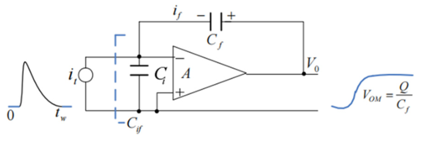
The working principle of CZT as a detector material involves the interaction of high energy radiation such as X-rays or γ-rays with the CZT crystal within a biased detector. When irradiated, the detector absorbs a portion or the entire energy of the incoming radiation. This absorption leads to the generation of electron-hole pairs within the crystal, proportional to the incident high-energy radiation. These pairs drift under the influence of an electric field towards different electrodes within the crystal. Eventually, they are collected on the electrodes [46]. Electric pulses are formed on the electrodes, and after passing through charge-sensitive preamplifier analog circuits, voltage pulses proportional to the energy of the incident radiation are output [47].
When high-energy radiation enters the CZT crystal and generates electron-hole pairs, use VB represents the bias voltage applied to the crystal and d indicates the thickness of the crystal, the electric field within the crystal can be expressed by the formula:
E = V B d
The charge drift velocity is as:
V = μ E = μ V B d
The induced current i can be obtained from Shockley-Ramo theorem using Formula:
i = E Q q v = 1 d q μ E = 1 d q μ E V b d = q μ V b d 2
If the electron-hole pairs generated by the radiation in the CZT crystal reach opposite electrodes, the distance of charge drift equals the entire thickness of the crystal, denoted as d. Thus, the time for charge drift to reach the electrode, the charge collection time can be expressed by formula [48]:
t = d v = d 2 V B μ e
The induced charge Q of the detector is as:
Q = i t = q μ V B d 2 d 2 V B μ = q
If the electron-hole pairs produced by the rays in the CZT crystal are at a distance of x from the anode, then the collection time of the electrons te
t e = x v e = x d V B μ e
The time of collection of holes is th
t h = d x v h = ( d x ) d V B μ h
The induced charges Qe and Qh generated by the two are respectively:
Q e = i e t e = q μ e V B d 2 x d V B μ e = q x d
Q h = i h t h = q μ h V B d 2 ( d x ) d V B μ e = q d x d
If the generation of electron-hole pairs occurs at the midpoint of the CZT crystal, then at the moment when the charges are fully collected:
Q e = Q h = q 2
Due to the migration efficiency of electrons being approximately three times that of holes μe≈3μh, the charges collected on the electrode are not entirely complete when the electrons have fully arrived. This incomplete charge collection is due to the extended collection time of holes, resulting in tailing effects in the final output signal. The collection time of the detector is correlated with the detector's thickness. Based on the specific thickness of the detector, an appropriate collection time can be calculated to facilitate the determination of specific subsequent circuit parameters. In 2009, L. Abbene et al. [49] conducted a study on the hard X-ray response of pixelated CZT detectors. Comparing detectors made in the same manner with identical materials but with CZT crystals of 1mm and 2mm thickness, the thicker detector exhibited better performance. This suggests that increasing the detector thickness improves both detection efficiency and charge collection, consistent with the small-pixel effect. To maximize the complete collection of generated charges within the lifetime of the hole, the charge collection time should be at least several times the electron collection time when the electron-hole pairs are at the midpoint of the detector. Determining the collection time provides a reference for establishing the pole-zero cancellation time and Gaussian shaping time, as these times must not be less than the charge collection time. Otherwise, it significantly affects the energy resolution of the detector system [50,51,52].

2.3.2. Research on the energy resolution of CZT materials

The energy resolution of a detector is a critically important performance indicator. As semiconductor materials form a crucial component of detectors, extensive research has been conducted on the energy resolution performance of CZT crystals.
In 2011, Kristen Wangerin et al. [53] studied three different geometries of CZT anodes and compared the energy resolution and absolute peak efficiency before and after data corrections. Following the correction of the test data, both the energy resolution and efficiency showed improvement. It was observed that detectors with a pixel pitch of 1.3mm, exhibiting the best small-pixel effect, presented superior energy resolution, with an optimal resolution of 5.1 keV [54] Beginning in 2008, A.E. Bolotnikov et al. from the Brookhaven National Laboratory [55] conducted research on extended defects in CZT crystals for γ-ray detectors. CZT material contains a high concentration of extended defects, especially tellurium inclusions, dislocation networks, grain boundaries, and subgrain boundaries affecting the device's energy resolution and efficiency. In 2014, Xu Huichao et al. [56] from Shanghai Jiao Tong University investigated the noise performance of CZT crystals. They studied the detector's geometric shape, detector voltage, and time constants. The incomplete charge collection within the detector crystal is the main factor affecting detector performance. The primary reason is that the product of the mobility and lifetime of holes in the material is one to two orders of magnitude smaller than that of electrons. A.E. Bolotnikov group from BNL [57] conducted research on charge loss under normal circumstances, as shown in the formula:
Q = Q 0 e x p ( t d r i g h f t τ b u l k )
Q and Q0 are charged and initial charges collected by the incident particle or photon, tdrigft is the drift time of the electron cloud from the interaction point to the anode, τbulk is the lifetime of the electrons in the CZT body. When a defect occurs inside the crystal, the charge is lost as:
Q = Q i { 1 η i 1 exp t i τ i }
ti and τi represent the electron drift distance and lifetime, they are averaged over the i geometric region. η i is a portion of the charge of the electron cloud passing through the encompassed geometric area. The integrated charge left behind in the electron cloud after encountering it is shown as:
Q = Q i { 1 η i 1 exp D i E i μ i τ i }
Ei is the local electric field strength, μiτi represents the attenuation distance, i denotes the average distance.
It has been observed through testing that the decrease in collected charge signal amplitudes due to tellurium inclusions is proportional to the electron cloud's drift distance.
Based on this, in 2015, the domestic team led by Wang Chuang [58] characterized the prepared CZT pixel detectors. They analyzed the impact of tellurium inclusions and other defects within the crystal on the electronic properties, such as detector leakage current and spectral response characteristics. The comparison revealed that enrichment of tellurium inclusions increased detector leakage current, reduced charge collection efficiency, and deteriorated the detector's energy resolution. In 2019, Fan Lei et al. [59], in an effort to enhance CZT's discrimination capability, introduced an improved method using 10B as a conversion layer for thermal neutron detection. The reaction of neutrons with 10B primarily generates energies of 2.792 MeV and 2.31 MeV:
n+10B→α+7Li+2.792 MeV( 6.1%)
n+10B→α+7Li* +2.31 MeV( 93.9%)
To achieve a higher energy resolution in CZT crystals, it is necessary to reduce the crystal's leakage current. This can be accomplished through surface treatments, optimized electrode designs, minimizing grain boundaries and defects, controlling impurity levels within the crystal, selecting appropriate sizes, and using high-quality crystals. These optimization methods are effective in enhancing the energy resolution of CZT crystals, making them more suitable for high-precision detector applications [60].
The thickness of the CZT itself also has an effect on the energy resolution of the detection system. In 2014, Shen Min et al. [61] conducted experiments and simulations on CZT crystals of different thicknesses using various radiation sources. They found a high level of consistency between theoretical and experimental values of energy spectra and peak efficiencies for CZT detectors of different thicknesses under different γ photon energy conditions. They noted that thicker CZT detectors achieved higher energy resolution and peak efficiency at higher energies, whereas thinner detectors exhibited relatively better characteristics at lower energies. Thin CZT crystals at 662 keV, using 137Cs as a radiation source, showed low photon attenuation characteristics. The conclusion drawn was that for detecting high-energy radiation, CZT crystals must have sufficient thickness to provide better accumulation of high-energy photons and improved detection efficiency. In 2021, Yu Hui et al. [62] from Northwestern Polytechnical University studied the impact of crystal thickness on the spectrum of CZT detectors. They found that as the CZT thickness increased, the peak height of the final image increased, the full width at half maximum (FWHM) decreased, the peak address decreased, and the total charge collection efficiency reduced.
In summary, to improve the energy resolution of detectors by enhancing CZT crystals, key methods include optimizing the geometric shape of the array to achieve the best small-pixel effect. Additionally, improving crystal performance and enhancing energy resolution can be achieved by changing semiconductor crystal thickness and optimizing manufacturing processes.

2.3.3. Research on the energy bands of CZT crystals

For the semiconductor crystal, when the energy of incident photons is greater than the bandgap width, electrons in the valence band are excited into the conduction band. Interaction between electrons and the crystal lattice causes electron transitions into the conduction band. The vacancies left by the departing electrons, known as holes, then transition back to the valence band. When the exciting photons are removed, the excess electrons and holes cannot maintain a thermal equilibrium state within the crystal. Consequently, they recombine. Electrons transition from the conduction band back to the valence band. As the scattering of photons must adhere to the conservation of energy and momentum, the scattered energy equals the difference in energy between the conduction and valence bands [63].
It has been found that Cd1-xZnxTe just like CdTe, is also a direct bandgap crystal. Because ZnTe (Eg=2.26 eV) has a larger band gap than CdTe (Eg=1.46 eV), so the inclusion of Zn elements will make the band gap of Cd1-xZnxTe larger than that of CdTe, and the band gap will change with the increase of zinc content. There are some differences in the results obtained by different researchers:
Table 3. Relationship between CZT band gap and Zn content and temperature [64,65,66,67,68,69,70,71].
Empirical formula Research Group Temperature
Eg (eV)=1.604+0.42x+0.33x2 Taguchi 9K
Eg (eV)=1.5964+0.445x+0.33x2 Doty 12 K
Eg (eV)=1.586+0.5006x+0.29692x2 77 K
Eg (eV)=1.4637+0.496x+0.2289x2 300 K
Eg (eV)=1.598+0.614x-0.116x2 Polichar
Eg (eV)=1.5+0.5x+0.2x2 Toney
Eg (eV)=1.5045+0.631x+0.128x2 Tobin
Eg (eV)=1.606+0.332x+0.462x2 Hoschl
Eg (eV)=(1.494±0.005)+(0.606±0.010)x+(0.139±0.010)x2 Li
For different temperatures T, the bandgap width of CZT also varies. At x=0.5, the relationship between the bandgap width and temperature can be expressed by Formula [72]:
Eg (eV)=1.72-3.5×10⁻⁴T-1.55×10⁻⁷T2
When the energy of incident photons exceeds the bandgap width, electrons in the valence band are excited to the conduction band. The interaction between electrons and the crystal lattice induces electron transitions to the conduction band. Vacancies left behind by the departing electrons, known as holes, subsequently transition back to the valence band [73].
In 2015, Guo Rongrong et al. [74] investigated the impact of sub-bandgap light on CZT crystal. They discovered that under external sub-bandgap illumination, the crystal's defect density decreased, leading to a more uniform electric field distribution and a reduction in the concentration of active traps. Additionally, measurements of the 241Am γ ray spectrum response by the detector confirmed that simultaneous illumination with sub-bandgap light significantly enhanced the energy resolution and charge collection efficiency of CZT detectors.
In 2022, Chen Xiang from the China Institute of Atomic Energy [75] conducted an optimization of the energy band structure of crystals, utilizing a CZT crystal with dimensions of 5mm×5mm×1mm provided by Shaanxi Detai Technology. Their study focused on the optimization of the γ sensitivity performance of CZT detectors, specifically addressing the issue of overshoot in the calibration current curves for CZT detector γ sensitivity. To address the trapping effect of deep-level traps on charge carriers within the crystal, the study employed sub-bandgap light to adjust the occupation of deep-level traps by charge carriers, thereby eliminating the overshoot in the calibration current curves of the detector. This approach increased the charge carrier collection efficiency, leading to the optimization of CZT detector performance. As a result, the particle sensitivity of the detector to γ rays with an energy of approximately 1.25 MeV reached1.18×10-16C·cm.
Optimizing the detector sensitivity by enhancing the energy band structure of CZT crystals has been proven to hold practical value. Further research in this area holds potential for additional exploration and investigation.

3. Development of CZT array detectors

3.1. Different structured CZT detector

3.1.1. CZT detector structure

The development history of semiconductor nuclear radiation detectors spans back to the 1960s and continues to progress significantly till this day. As early as 1949, researchers discovered that Ge diodes produced a pulse output when exposed to α particles. Subsequently, a variety of radiation detection materials and devices were introduced. Presently, commonly used semiconductor radiation detectors mainly include the PN junction detector, silicon lithium-drifted detector, high-purity germanium (HP-Ge) detector, and compound semiconductor detectors. In the realm of compound semiconductors, significant research focuses on materials like GaAs、CdTe、CdZnTe、SiC which CZT materials hold a significant position [76].
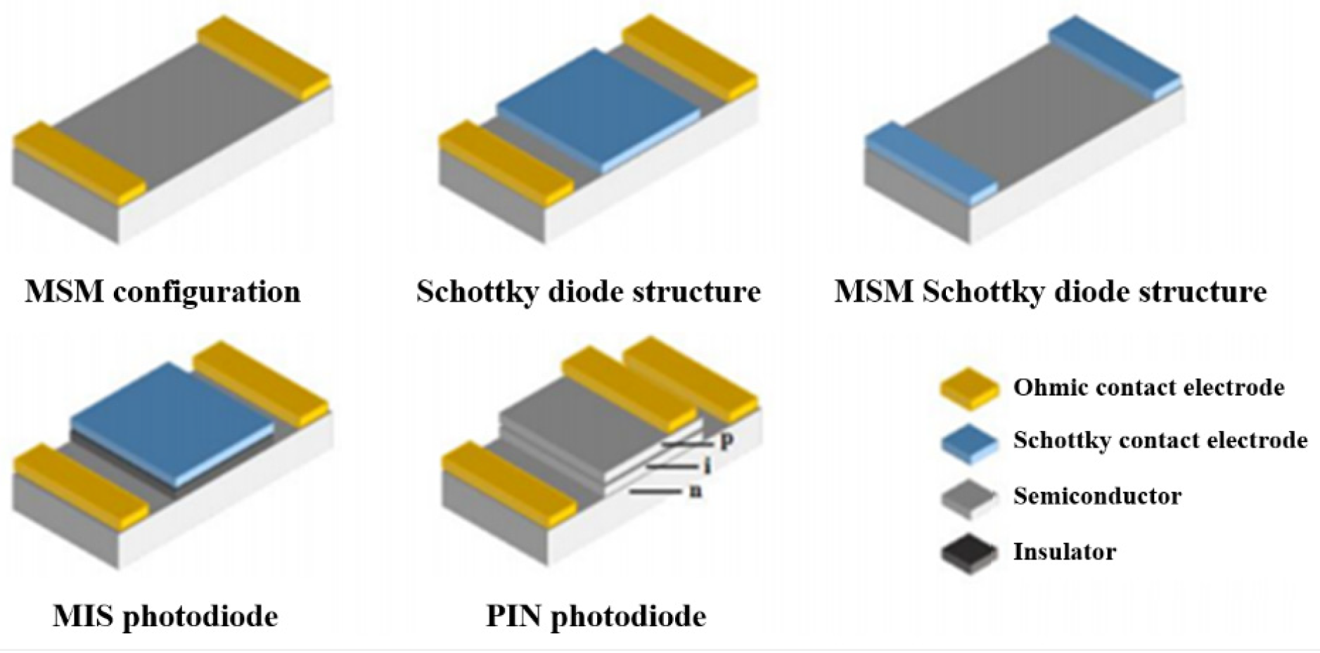
The configurations of photodetectors vary and can be broadly classified into two main categories based on their photocurrent mechanisms: photodischarge devices and photovoltaic devices. Photodischarge devices feature a structure with an anode and cathode forming an ohmic contact MSM (Metal-Semiconductor-Metal) configuration. Generally, the active region in this structure is the surface layer that receives the incident radiation. Its advantage lies in its relatively better photoresponse in short wavelengths. However, due to the presence of ohmic contacts, this configuration may exhibit higher dark currents and lower device sensitivity, as well as slower response speeds.
Photovoltaic devices consist of various structures such as Schottky diode structure, MIS structure, PN junction structure, PIN junction structure, and avalanche photodiodes (APD). In comparison to photodischarge detectors, the active region of photovoltaic detectors penetrates deeper into the semiconductor. This allows for thickening the active region through structural design or increased reverse bias, thereby enhancing the device's quantum efficiency. Due to the presence of the Schottky or PN, these devices typically exhibit lower dark currents and faster response speeds. Based on their operational principles, photovoltaic devices can be further divided into two categories: depletion-type and avalanche-type. Depletion-type devices involve the process of photon-to-electric conversion occurring in the depletion layer, with photocurrent primarily generated by the drift of photo-generated charge carriers. Common examples include Schottky diodes, PN junctions, and PIN structures. On the other hand, avalanche-type devices, as implied by the name, operate in the avalanche region, where photocurrent gain is primarily generated through the avalanche effect, as seen in APDs. While these devices offer significant internal current gain, they demand strict requirements in terms of materials and device properties [77]. Illustrations of various photodetector configurations are depicted in the Figure 2
In materials like CZT, the electron mobility is approximately 1100cm2/V·s with a migration lifetime of around 2 μs, whereas the hole mobility is about 100cm2/V·s with a migration lifetime of approximately 0.05 μs. The significant disparity in the mobility abilities of electrons and holes implies that holes are captured extensively. As per the Hecht equation (Formula 17), the induced charge collected by the electrodes is dependent on the distance traveled by the corresponding charge carriers within the crystal. The substantial capture of holes results in incomplete hole signals collected by the cathode. In contrast, due to their longer migration lifetime, electrons can be fully collected by the anode. This asymmetry in collection leads to an asymmetric signal peak, shifting towards the lower energy region. Consequently, this effect, known as the hole tailing effect, reduces the energy resolution [78].
Q = N 0 e [ λ e d 1 e x c λ c + λ e d 1 e x h λ h ]
N0——Number of electron-hole pairs;
d——Detector thickness;
λ——The drift length of the electron with the hole;
x——The length of the drift that the electrons must do with the holes.
To address the issue of low energy resolution caused by the hole tailing effect, research primarily employs two main categories of methods: correction of pulse signals through electronic methods and adjustments made in the electrode structure to achieve unipolarity [79].
The adjustments made in the electrode structure primarily rely on unipolar charge induction. According to the Shockley-Ramo theorem, the induced charge on the electrode is directly proportional to the change in the weighted potential as the charge q moves from the starting point to the ending point [80,81].
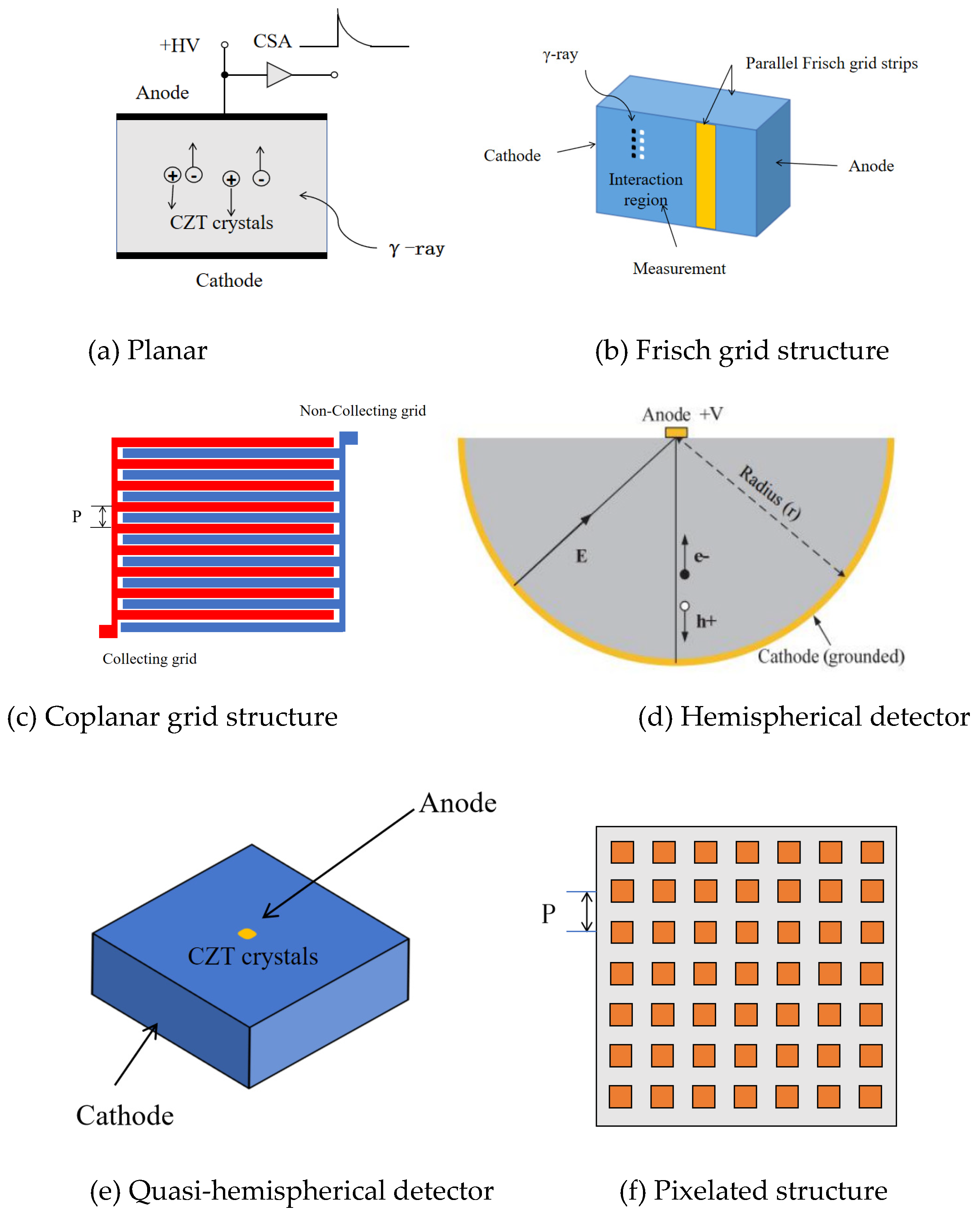
The adjustment in the electrode structure aims to eliminate the electrical signals generated by hole drift, thereby focusing on collecting the signals generated only by electron drift to enhance energy resolution. Presently, the primary electrode structures for CZT detectors include planar, Frisch grid structure, coplanar grid structure, pixelated structure, hemispherical detector, quasi-hemispherical detector, and others as illustrated in Figure 3 [11]:
The planar structure is the simplest configuration, as depicted in Figure 3(a). In a planar CZT detector, metal is deposited on both sides of the CZT crystal, forming a metal-semiconductor-metal structure. When high-energy radiation penetrates the CZT crystal and exceeds the material's bandgap, it excites electrons from the valence band to the conduction band, thereby creating electron-hole pairs. Under the influence of the electric field from the electrodes, electrons and holes are collected to induce charge. However, this method faces issues as the electron mobility in CZT is significantly higher than that of holes. Consequently, holes are more susceptible to capture by impurities and defects within the crystal, resulting in non-uniform collection of electrons and holes at the electrodes [82].
The Frisch grid structure, illustrated in Figure 3(b), involves creating a Frisch ring electrode near the anode position on the side of the CZT detector and grounding it. Under a specific external bias, the electric field in the device primarily exists between the grid and the anode. Given that radiation photons enter from the cathode and stop within the CZT near the cathode, it is apparent that only electrons passing through the annular surface of the Frisch grid can go through the electric field region and induce charge. This design excludes any induced signals generated by charge movement between the cathode and the Frisch grid, allowing the collected signals from the device to be considered as generated solely by electron drift. This effectively eliminates the hole tailing effect [83].
The coplanar grid structure, as shown in Figure 3(c), involves creating two sets of interdigitated comb-like strip electrodes on the anode, applying different voltages to these two grid electrodes. The grid with the higher potential is referred to as the collecting electrode, while the one with the lower potential is known as the non-collecting electrode. This structure generates a stronger electric field near the anode, leading to a rapid change in the weighting potential. Conversely, the weighting potential change near the cathode tends to be more gradual, thereby reducing the electric signals produced by hole drift near the cathode. As the distance between the coplanar grid electrodes decreases, the charge collection becomes more uniform. However, a smaller electrode distance may result in higher surface leakage currents in the device [84].
The hemispherical detector is one of the earliest unipolar semiconductor radiation detectors, with an ideal structure depicted in Figure 3(d). The quasi-hemispherical and hemispherical structures are similar in principle. Due to the difficulty in manufacturing true hemispherical crystals, a simplified cubic shape is often used to represent the hemispherical structure, as illustrated in Figure 3(e). All four lateral surfaces and the bottom surface act as cathode surfaces, while the anode contact is situated in the center of the anode surface. This structural setup results in a strong electric field near the anode, with a steep rise in the weighting potential. Meanwhile, the electric field and weighting potential near the cathode are relatively flat, effectively reducing the impact of hole drift on the electric signal generation process [85].
Array-type detectors, illustrated in Figure 3(f), consist of a grid of equally sized squares forming the anode surface. Each square represents a small pixelated anode. During operation, the pixelated anodes are connected to a high voltage, while the cathode plane is grounded. As electrons move away from the anode, all pixel arrays produce weak signals. When electrons move closer to the anode, the signals of the other pixel detectors gradually decrease, while the signal from the corresponding pixel detector position continually increases until reaching its maximum value. Similarly, the weighting potential changes slowly near the cathode and dramatically increases near the anode [86]. It's important to note that the smaller the pixel size, the higher the spatial resolution achieved, but this also increases unipolarity. However, this comes at the cost of reduced signal-to-noise ratio and decreased charge collection efficiency, known as the small pixel effect. Similar to the configuration of a co-planar grid, reducing the pixel size is also accompanied by a significant increase in surface leakage current [87].
Among all unipolar structures, the pixelated configuration performs the best and has the most mature processes. The performance of the detector unit is directly related to the size of the pixel; smaller pixels exhibit better unit performance, a phenomenon referred to as the "small pixel effect" [88]. Pixelated CZT detectors are commonly used in two-dimensional imaging and, when combined with depth sensing techniques, allow for three-dimensional imaging. This integration enhances energy resolution, offering a wide array of potential applications [89].

3.1.2. Operating principle of the CZT array detector

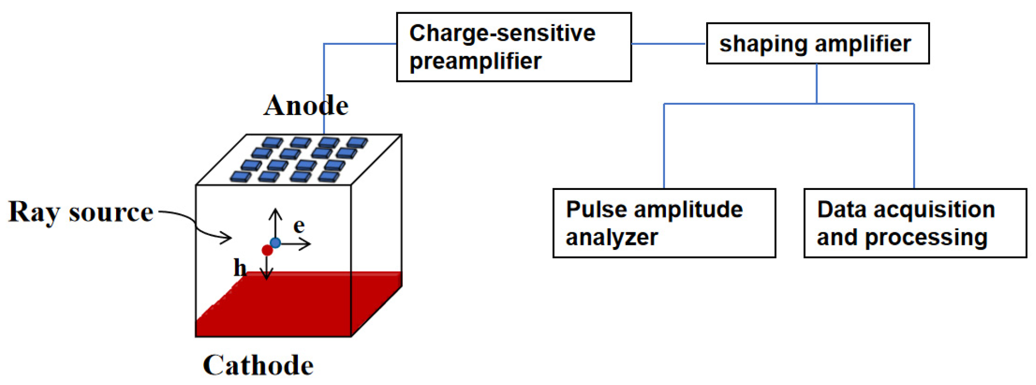
The operating principle of the CZT array detector involves segmented electrode design on one side of the CZT crystal, creating a pixel array electrode structure on the crystal's anode surface, while the cathode comprises a solid plane electrode. When radiation enters from the cathode surface, a negative high voltage is applied to the cathode surface. The ionizing radiation interacts with the crystal, generating numerous electron-hole pairs. Under the influence of the electric field formed by the applied bias, the electrons and holes migrate towards their respective poles. The induced charges are collected by the pixel electrodes. They are then converted into voltage pulse signals proportional to the amplitude and energy of the incident photons by a charge-sensitive preamplifier. Subsequently, shaping amplifiers further amplify these signals to enhance the signal-to-noise ratio. Finally, the signals can be utilized to generate corresponding spectral distributions or, through signal acquisition and processing, to create images based on the pulse amplitude distribution statistics [90].
The radiation enters from the cathode surface while applying a negative high voltage on the cathode surface. The ionizing radiation interacts with the crystal, creating numerous electron-hole pairs. Under the influence of the externally applied bias, the electric field is established. Electrons and holes migrate towards their respective poles, generating induced charges collected by the pixel electrodes. These charges are converted by the charge-sensitive preamplifier into voltage pulse signals proportional to the amplitude and energy of the incident photons. Subsequently, these signals are further shaped and amplified by a shaping amplifier to achieve higher signal-to-noise ratios. Finally, the signals can be used to derive the corresponding spectral distributions through statistical analysis of the pulse amplitude distribution or processed to generate images after signal acquisition and processing. The schematic diagram depicting its operation is illustrated in Figure 4
The electron-hole pairs move towards different electrodes under the external bias of the detector and are eventually collected. These signals can be used to form the energy spectrum of incident photons via a multi-channel analyzer. In the study of array detectors, the assessment criteria for the detector's performance include noise, energy resolution, response speed, and other aspects. These criteria are interdependent, mutually constraining one another. Therefore, it is important to individually analyze various influencing factors.

3.2. Research on the performance optimization of CZT array detectors

3.2.1. Optimization of energy resolution

The energy resolution refers to a detector's actual ability to distinguish nuclear information and is generally defined as the smallest relative difference between the energies of two adjacent values for a given energy. Due to statistical fluctuations in the detection process, even for a single nuclear radiation energy, the relationship between the collected count rate and energy is not a straight line but a distribution curve. Therefore, the Full Width at Half Maximum (FWHM) of this curve, indicating the width of the curve at its half maximum, is often used to represent the characteristics of resolution [92].
When CZT detectors operate at room temperature, the leakage current is one of the primary parameters determining the detector's performance. As unipolar detectors only collect signals generated by electron carriers, excluding the impact of holes, the signal induced by electrons in the detector's electrodes is proportional to the total charge generated by photon deposition. The effect of holes depends on the detector's structure and the generation position of electron-hole pairs. It has been demonstrated that uncollected holes can affect the detector's performance, reducing the energy resolution, particularly evident in planar detectors. Smaller anode arrays can decrease the influence of holes, enhancing collection efficiency and energy resolution while also achieving relatively higher spatial resolution with a simple structure.
In 2005, the research team led by A.E Bolotnikov [93] investigated the primary factors influencing the energy resolution of CZT detectors. The study explored three key factors that limit the performance and ultimate energy resolution of CZT devices:
  • Impact of leakage current: In CZT devices with Au and Pt contacts, the overall leakage current is restricted by the characteristics of the Schottky barrier at the metal-semiconductor interface.
  • Influence of charge sharing among pixels: Inter-pixel electric conduction affects the distribution of electric field lines, leading to charge loss between adjacent anode contacts in multi-electrode devices.
  • Effects of charge loss: Charge loss usually accompanies charge sharing. Some electrons in the electron cloud between pixels fall into the gap and remain uncollected by the pixel electrodes, resulting in charge loss.
In 2012, the team [94] conducted research on the energy resolution of CZT detectors, improving the application-specific integrated circuits (ASIC) and data acquisition systems originally used for 3D pixel detectors. They introduced a universal cathode readout system to correct charge signals and eliminate incomplete charge collection events. The study evaluated a 2x2 size, 6x6x15m3virtual flash grid detector array and found that in applications requiring lower position and energy resolution, large-pixel, low-density array formats might replace more advanced but costlier 3D pixel array detectors. Furthermore, the large-pixel, low-density array offered improved energy resolution, higher stopping power, and position resolution. It was demonstrated that by employing a cathode signal readout system, incomplete charge collection events due to crystal defects could be filtered out. Thus, it became feasible to utilize crystals with some defect content at a lower cost for manufacturing such arrays [95].
In 2007, Wilson et al. [96] measured the signal shapes produced by alpha and X-ray radiation in a 2mm-thick CZT detector. They compared the signals generated by a single large substrate detector and a 300μm pixelated detector. Eventually, they used TCAD simulation software to directly compare experimental data, allowing for the visualization of carrier motion within the CZT detector. This visualization helped determine that the primary cause of charge sharing events is the initial size and subsequent diffusion of the carrier cloud.
In 2011, the team led by Jiang et al. [97] conducted research on the noise performance of cadmium zinc telluride (CZT) array detectors. They employed low-noise fast preamplifier modules, analyzed the internal performance of the crystal, and investigated the impact of the preamplifier on the noise of the detection system. They established a 2×2 cadmium zinc telluride pixel array detection system. Experimental results showed that the output signal noise of the detection system was minimal, with no pulse pile-up. The electronic noise of the readout circuit was significantly suppressed, resulting in reduced low-energy tailing in the spectra. Improvements were noted in the noise caused by incomplete charge collection and leakage current noise. The team also conducted a noise analysis of the entire system and the preamplifier, proposing relevant improvement methods that effectively suppressed the electronic noise of the readout circuit.
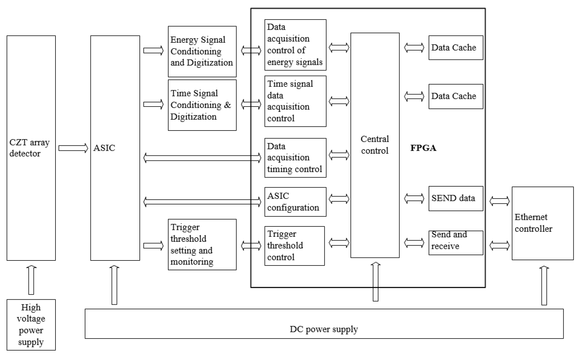
In 2022, Wang Wei et al. [98] designed critical circuits in both single-channel and sixteen-channel readout circuits to mitigate the impact of leakage current on the detector's energy resolution. The single-channel readout circuit comprises CSA, SHAPER, DIS, and PDH modules. Additionally, to suit the specific application scenario of SPECT, they added leakage current compensation circuits and baseline holding circuits based on the traditional single-channel design. They further designed a loop bias module, enhancing the electronic design of the detector. As a result, they achieved a maximum compensation of 50nA for leakage current, a peaking time of 150ns, a channel gain of 50mV/fC, less than 1% integral non-linearity, and a maximum injection frequency of 500kHz.
At the charge sharing optimization realm, in the last century, A.E Bolotnikov and colleagues [99] discussed the charge loss between pixel detector contacts and studied several different gap contact arrays' charge loss on a CZT detector. They identified the maximum contact gap at which the charge loss between surface pixels could be neglected. They discovered that the minimum signal loss occurred with a contact size of 450μm and a distance of 50μm between contact edges. As the array gap increased, there was a rapid increase in signal loss, and there was the appearance of pixel channel dead zones in the array gap [100]. In 2007, the research group also designed a hexagonal grid CZT crystal virtual flash grid detector to evaluate the performance of the CZT detector's basic design from the perspective of the residual effect of uncollected holes in the CZT detector. In practice, it is not feasible to entirely shield the charge caused by uncollected holes in the entire active volume of the device. However, in the CZT detector's design, it is possible to correct the output signal changes in the drift region while rejecting interaction events from the induction region.
In 2007, Kris Iniewski et al. [101] proposed an analytical model to provide an effective framework for studying the influence of detector geometry, bias conditions, and material properties on detector performance. The model accurately predicted the number of charge-sharing events as a function of photon energy and detector pixel size. Simulations were performed on a material with a Cd0.9Zn0.1Te composition. Comparative results revealed that a higher number of sharing events occurred when the gap between 0.46 mm-sized pixels was larger than 0.1 mm and increased with the radius "r" of the electron cloud. Additionally, it was determined that corner pixels within the array exhibited fewer sharing events compared to edge pixels, while edge pixels exhibited fewer sharing events compared to center pixels. The energy resolution (FWHM) was poorest for corner pixels, followed by edge pixels, with the center pixels demonstrating the best energy resolution. In 2009, Yongzhi Yin and colleagues [102] characterized high-resolution CZT detectors for sub-millimeter PET imaging. Their research discovered that the ratio of events between central single-pixel events and central double-pixel events decreased when the radiation energy increased from 59.5 keV to 122 keV. As the pixel array size became very small (350 μm), the impact of charge sharing on detector energy resolution might be more critical than the small pixel effect. The team measured the distribution of charge-sharing events and combined them with collimated beam size and their contribution to charge sharing. Under detector conditions with a 600 μm spacing and 5 mm thickness and a 350 μm spacing, the optimal gap for charge sharing in the measurement of a 122 keV collimated beam was approximately 125 μm.
In 2011, MC Veale et al. [88] discussed the charge sharing effects in small-pixel CZT detectors. They employed ASIC software developed by the Rutherford Appleton Laboratory to compare the amount of charge sharing under various anode geometric shapes. Their study concluded that in comparison to array detectors with the same pixel size but different spacings, the shape of the final spectrum is influenced by increased charge sharing in the anodes. Consequently, arrays with larger spacings exhibited a decrease in the amplitude of the main peak relative to the lower energy peaks.
In 2007, the team led by A.E Bolotnikov [103] discussed the performance of a 20x20x10 mm³ and 10x10x10x10 mm³ single-pixelated detector, as well as a 4x4x12 mm³ virtual flash grid device. They detailed various physical properties of the materials and proposed the concept of "small gaps" as a solution. Their findings revealed that reducing the gaps between pixels effectively reduces charge loss. When the gap size is reduced to below 100 μm, it achieves an effect similar to that of the guard ring.
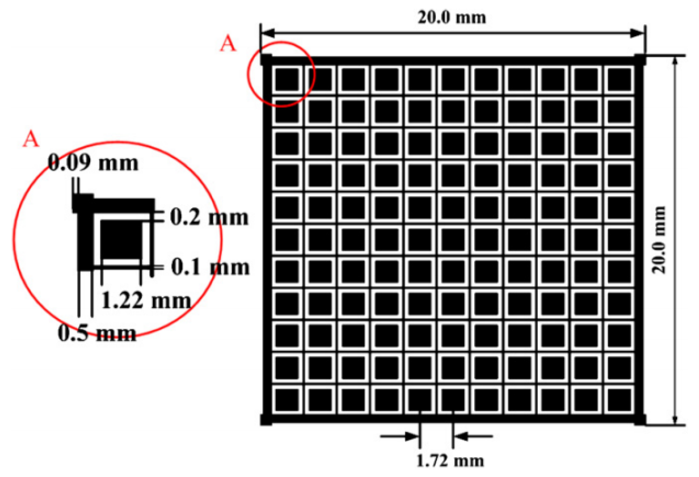
As the crystal array's reduced spacing could result in the occurrence of charge-sharing events, in 2011, JC Kim and colleagues from the University of Michigan proposed an enhancement approach for pixelated cadmium zinc telluride (CZT) detectors by designing a guiding ring. This involved the addition of extra electrodes between the gaps, as illustrated in Figure 5
The design of the guiding ring typically encircles each pixel, to some extent improving the edges. To ensure that the electron cloud (charge carriers) between the pixels is collected by the pixel electrodes under the influence of the electric field, the guiding ring's width needs to be minimized while applying adequate negative high voltage. However, this introduces surface leakage currents between the pixel electrodes and the guiding ring, leading to increased electronic noise in the pixel anode and consequently a reduction in energy resolution to some extent. This method presents challenges in fabrication. Imperfect electrode processing can result in low surface impedance, causing excessive surface leakage currents and potentially leading to certain pixel channels becoming non-functional. In the absence of sufficient bias, significant charge loss phenomena might occur.
In conclusion, to enhance the overall energy resolution of the array detector, improvements are required not only in the crystal performance but also in the channel-level performance of the detector. Enhancing the contact methods between various components, such as by refining the readout circuitry and implementing guiding rings, reduces the loss during charge transfer, thus elevating the final energy resolution.

3.2.2. Research on the spatial resolution of array detectors

High-energy radiation imaging detection has been a highly researched topic in various fields such as high-energy nuclear physics, astrophysics, and nuclear security detection both domestically and internationally. A 3D position-sensitive CZT room-temperature γ ray spectrometer typically comprises an array detector crystal with independent pixelated anodes and dedicated channels for signal processing. Each channel includes an integrated circuit for readout, incorporating a preamplifier, a shaping amplifier, and a sample-and-hold device. The depth of γ ray penetration is determined by the ratio of the cathode to anode signals from each pixel [105]. For obtaining high-quality images, the primary technical requirements for array detectors include high detection efficiency and sensitivity for high-energy or γ radiation. Additionally, a large signal dynamic range, indicated by the ratio of the maximum output signal (open-circuit signal) to the system's noise, is necessary. Good isolation between pixels is crucial to eliminate signal interference among pixels, and appropriate pixel size is essential [106].
In 2009, a collaborative effort between NASA and Lawrence Livermore National Laboratory (LLNL) [107,108] led to the establishment of a large-area 128×128 pixel 32cm×32cm high-energy CZT pixel array imaging detection system. This system covered the energy range from 10 to 600 keV. It achieved an energy resolution of 5.37% for 241Am and a spatial resolution of 2.5 mm.
In 2012, Feng Zhang et al. [109] characterized detectors using a new application-specific integrated circuit (ASIC) developed by the Brookhaven National Laboratory's Instrumentation Division. Their findings revealed that the energy resolution of three-dimensional position-sensitive CZT detectors does not necessarily decrease with an increase in detector volume/thickness. The excellent energy resolution of the detector indicates that large-area CZT detectors can approach the theoretical limits of energy resolution.
In 2012, Yongzhi Yin et al. [110,111,112] conducted a study on three significant factors influencing the three-dimensional spatial resolution of 350 μm pitch CZT array detectors. These factors included charge sharing, intrinsic spatial resolution measurements, and Depth of Interaction (DOI) analysis. They found that with an increase in γ-ray energy, the number of charge-sharing events in double-pixel arrangements notably increased. This indicates a larger charge cloud size and a higher probability of Compton scattering resulting from higher energy γ rays. Additionally, they observed a linear relationship between the γ-ray electron drift time and the cathode/anode ratio.
In 2018, Ukaegbu I K et al. [113] from the School of Engineering at the University of Glasgow in the UK developed a decay model for Cadmium Zinc Telluride (CZT) detectors. This model aimed to estimate the depth of remotely buried radioactive waste. Through a comparison with an organic liquid scintillator detection system, the established model was capable of estimating the depth of a 329 kBq 137Cs radioactive source buried within a 12-centimeter-thick layer, yielding an average count rate of 100 counts per second. Experimental validation using a 9 kBq 60Co radioactive source affirmed that the model could be applicable for any γ radiation source. Furthermore, it demonstrated the ability to estimate the depth of buried sources with extremely low activity.
In 2022, a team led by Pan Chao from the China Academy of Launch Vehicle Technology [114] proposed a method for implementing a multi-beam array detection three-dimensional imaging lidar system. Their study involved research into this system and its performance, as well as the analysis of errors through computer simulation. This work aimed to provide a theoretical foundation for the design and parameter optimization of multi-beam array detection three-dimensional imaging lidar systems.
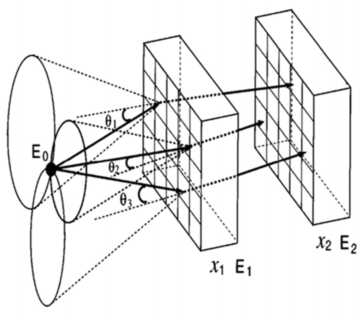
In 2000, He Zhong and colleagues from the Department of Nuclear Engineering and Radiological Sciences at the University of Michigan [115,116] introduced a general technique to address carrier capture issues, including hole and electron capture. This method involved determining the depth of interaction (DOI) information for each event, followed by the correction of different positions' charge collection efficiencies, resulting in uniform charge collection efficiency throughout the entire detector. This approach is known as Depth Sensing and Correction (DOI correction). When implemented in pixel detectors, it can determine three-dimensional information about the interaction position. Pixel detectors are typically designed for imaging. To acquire depth information, Li Wen et al. [117] proposed a signal modeling method used to calibrate the relationship between C/A values and the depth of interaction. The process involved assuming equal gains for cathode and anode electronics, depositing energy at different depths, calculating the corresponding cathode and anode signal amplitudes, and finally plotting the relationship between C/A values and the depth of interaction.
In 2006, Liptac, J et al. [118] employed fast digitization and software signal processing techniques using the HXR diagnostic method to image the energy of a CZT detector system containing 32 arrays within the 20-200 keV range. By comparing spectra between different channels, they obtained spatial information about fast electron clusters.
In 2010, Emerson Vernon et al. [119] introduced an improved Application-Specific Integrated Circuit (ASIC) designed for Three-Dimensional Position Sensitive Detectors (3D PSD). By altering the anode channels to process two polarity events simultaneously and store amplitudes in the corresponding positive and negative peak detectors, they addressed the issue of additional counts above the photopeak for energies higher than the light peak. By increasing the number of anode channels to 128 while maintaining symmetrical layouts, the new detector required 2 ASICs to read out a 256-pixel sensor, measuring peak amplitudes and relative timings for 128 anodes, one anode, and the cathode. The shaped analog signals from each channel could be multiplexed to an auxiliary output for monitoring purposes. The multiplexing and readout logic was optimized to reduce dead time and achieve higher count rates.
In 2021, Youngjin Lee et al. [120] utilized Geant4 simulations in combination with an enhanced median Wiener filtering technique and edge detection methods to improve the quality of the fused γ-ray and X-ray images obtained from CZT detectors. They demonstrated that the method combining MMWF and edge detection algorithms showed superior filtering performance in γ-ray and X-ray fused images produced by photon-counting CZT detectors compared to traditional methods.
In three-dimensional CZT detectors, the amplitude of induced signals depends on the Depth of Interaction (DOI). Therefore, the calibration of detectors using the Depth of Interaction correction technique plays a crucial role in improving the energy resolution of γ-ray detectors. Li Y [121] from Nanjing University of Aeronautics and Astronautics conducted research on existing DOI correction methods and proposed an improved energy correction algorithm. The experimental study discussed DOI correction factors for CZT detectors at various energy levels. By utilizing a segmented energy correction method, the research significantly improved the energy resolution and peak height of multiple energy peaks in the energy spectrum, achieving good correction results in multi-energy γ-ray detection. Furthermore, the research extended the DOI correction method for use in Compton imaging γ detectors, resulting in a noticeable enhancement in the image intensity for Compton imaging.
To enhance the spatial resolution of CZT array detectors, the primary research focus lies in refining the signal readout circuitry and optimizing algorithms, particularly emphasizing improvements in energy calibration algorithms. Such enhancements hold significant importance for improving the spatial resolution of the detector and the overall quality of imaging.

3.2.3. Optimization of detection efficiency

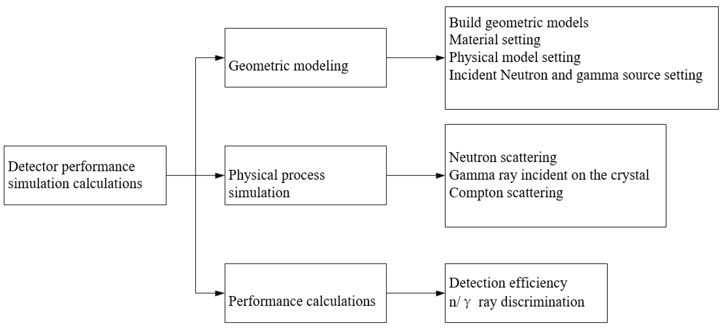
Lianjun Zhang and colleagues from the China Institute of Atomic Energy [122] developed and simulated a large-area array neutron-γ detection system based on plastic scintillator materials for specific nuclear material detection applications. They utilized Geant4 for initial structural optimization by simulating key detector components. The specific workflow for structural optimization is illustrated in Figure 6:
The simulation involved comparing the detection response threshold and the n/γ discrimination ratio before and after applying different thicknesses of lead and tungsten for shielding. The comparison revealed that, within a certain range, increasing the thickness of the shielding material gradually increased the n/γ discrimination ratio. Due to lead's lower ability to attenuate neutrons compared to tungsten, different thicknesses of lead provided a higher n/γ discrimination ratio. The simulation optimization results indicated that for a plastic scintillator with a 25μm thick Gd2O3 layer, and when the detection response threshold was set at 3, with a 3mm-thick lead plate between each layer of detectors, the system achieved approximately 23% neutron detection efficiency and an approximate 8/2 n/γ discrimination ratio. This ratio was roughly twice as high as that without any shielding material. This implies that improving the surface structure of the array detectors and adding shielding layers can enhance detection efficiency and the n/γ discrimination ratio.
In 2009, Lan Zhang et al. [124] conducted research focused on low-noise, stable performance thick-film circuits, achieving an energy resolution of 4% for the 241Am 60keV energy peak.
In 2017, Lei Fan et al. [59] used 10B as a conversion film and conducted a simulation analysis of CZT crystals using the MCNPX software. They found that the total detection efficiency and alpha (α) detection efficiency of the crystal gradually increased within the range of coating thickness from 0 to 1.6μm, reaching a peak at a thickness of 1.6μm. At this point, the total detection efficiency was 4.55%, while the α particle detection efficiency was 3.63%. This demonstrates that CZT requires a coating thickness of only 1.6μm to achieve maximum detection efficiency, offering conditions for manufacturing compact portable neutron detectors.
In 2018, Fayuan, Xi and their team [125] studied the influence of crystal thickness on the detection efficiency of CZT detectors. Due to the challenges in growth technology, it is difficult to produce larger single crystals greater than 1 cm in size with high-quality cadmium zinc telluride (CZT), resulting in increased costs. The efficiency of crystal detectors in detecting X-rays and γ rays depends on the crystal's thickness. For instance, a 1 mm thick CZT detector has a photoelectric absorption efficiency of 97.4% for 60 keV γ rays, which reduces to 58.3% for 100 keV γ rays. When the detector thickness increases to 4 mm, the photoelectric absorption efficiency for 100 keV γ rays improves to 97.07%. However, there's a notable decrease in detection efficiency for higher energy 662 keV γ rays. Therefore, CZT detectors are generally limited to detecting X-rays and γ-rays in the medium to low-energy range (10-600 keV), making it challenging to efficiently detect high-energy photons.
The study investigated the impact of cadmium zinc telluride (CZT) thickness and coating on crystal performance. By analyzing the response to γ-ray spectra, it was observed that in the higher energy range, increasing the thickness of the detector crystal to a certain extent or layering could result in improved detection efficiency and peak efficiency compared to a single-layer detector. The Compton continuum could also be improved, offering performance close to that of an entire CZT detector with equal thickness. However, the collection efficiency of photo-generated charge carriers decreased. The research demonstrated that the preparation of multilayer CZT detectors or the optimization of detector crystals to enhance detection efficiency is feasible but requires a comprehensive consideration of various impacts.

3.3. Array Detector Electronics

3.3.1. CZT crystal contact electrode

As the initial link in the signal transmission of a detector, the interface characteristics between the semiconductor crystal and the electrode play a crucial role in the detector's performance. The mutual diffusion between the metal electrode material and CZT, along with the defects at the interface, are important areas of study.
Regarding electrode contact, as early as 2000, A.E Bolotnikov et al. [126,127] conducted research on the influence of the geometric shape of the contact position on charge collection. They employed an orthogonal thin strip contact design between pixel contacts, applying a negative bias on the grid relative to the pixel potential to induce charge drift towards the contact point. This reduced the impact of charge loss between pixels, without significantly increasing leakage current, thereby enhancing the overall energy resolution of the detector.
In 2004, researchers led by Binsheng Wen at Shanghai University [128] prepared CZT crystals with electrode layers composed of Au, Al, and In on both sides. After comparison, it was determined that the chemically inert Au-sputtered electrode is more likely to form quasi-ohmic contact on p-type high resistivity CZT compared to other related electrodes, resulting in better crystal resistivity.
In 2010, Xiaoyan Liang et al. [129] conducted a study on the electrode contacts of CZT detectors. They examined the contacts of Au-CZT and Au/Cr-CZT through stress simulations and multi-channel spectral analysis. The results demonstrated that using Au/Cr composite electrode materials can enhance the adhesion strength and thermal stability of the electrodes.
In 2016, U. N. Roy et al. [130] investigated the surface treatment of Cd0.9Zn0.1Te detectors by depositing AZO (Al:ZnO) thin films on the surface using atomic layer deposition (ALD) technology. The study affirmed that AZO serves as a promising alternative contact layer for CdTe based room-temperature-operating nuclear radiation detectors. Zinc oxide offers advantages such as higher hardness, better chemical stability, closely matched thermal expansion coefficients with CdTe/CdZnTe, among other qualities. Detectors with AZO contact points demonstrated improved sensitivity and higher spectral performance.
In 2019, Liwen Ling et al. [131] conducted a study on the impact of Au/Cd composite electrodes on the conductivity of CZT crystals. The results indicated that direct deposition of Au electrodes on the crystal surface caused lattice damage to the CZT, forming an amorphous layer, which was unfavorable for Ohmic contact formation. The study found that the addition of a Zinc (Zn) intermediate layer at the Au/Zn-CZT interface was beneficial in eliminating the amorphous layer and promoting the formation of Ohmic contact. Furthermore, the deposition of a Cd layer on the surface of CZT chips resulted in the formation of a CdTe buffer layer, aiding in the elimination of the negative impact of Te-rich layers on the Au/CZT contact, thereby enhancing the electrode performance.
In summary, the interface properties of the contact electrodes in semiconductor crystals play a crucial role in the performance of detectors. The selection of different electrode materials and their geometrical shapes significantly impacts the charge collection efficiency and energy resolution. Some studies have shown that using composite electrode materials, such as Au/Cr, can achieve better quasi-Ohmic contact, thereby enhancing the electrode's adhesion strength and thermal stability. Additionally, methods involving the introduction of intermediate layers or the replacement of contact layers with thin films of zinc oxide (AZO) can improve the performance of CdTe-based nuclear radiation detectors, enhancing detector sensitivity and spectral capabilities. These investigations provide valuable insights into electrode design and performance optimization in CZT semiconductor materials, potentially driving further advancements in semiconductor detector technology.

3.3.2. Readout circuitry

The CZT pixelated array detector system primarily comprises the X-ray or γ-ray sources, the CZT detector, a high-voltage power supply capable of providing stable voltage, the readout circuitry for analyzing and processing the weak signals outputted by the detector, analog-to-digital converters for data acquisition, and PC-based image processing software [132].The front-end analog signal readout electronics system consists of the charge-sensitive preamplifier, which amplifies the weak charge signals from the detector, the shaping amplifier that filters and shapes the output pulse signal into quasi-Gaussian waveforms, analog-to-digital converters for data acquisition, and PC-based image processing software [133].
In a CZT pixel array detector, a corresponding number of charge-sensitive preamplifier circuits are required for each pixel to perform the pre-amplification processing of the weak electrical signals collected by each individual pixel. Subsequently, these signals are shaped into quasi-Gaussian waveforms by filtering and shaping amplification circuits. The information obtained from these procedures is then processed by a multi-channel analyzer to derive the energy spectrum of the incident photons [134].
When spectral detection is required, there are primarily two approaches for the design of the detector's readout circuitry. The first involves the use of a design based on mature large-scale integrated circuits. This approach is associated with higher costs, longer development times, and more demanding technological requirements. The second approach employs a design based on discrete components for the readout circuit. This method is characterized by lower costs and greater design flexibility, allowing continual refinement of the design during the circuit's design and production process, which can result in relatively good technical specifications. However, circuits produced by this method have lower integration levels and larger physical volumes [135].
The electrical signal output from the detector upon exposure to X-ray and γ-ray radiation is pre-amplified by a preamplifier and transformed into an exponentially decaying signal with a long time constant. This pulse signal, after passing through a pole-zero cancellation circuit, undergoes a downswing elimination, narrowing its width. The processed signal then passes through multiple stages of filter circuits for shaping, converting the pulse signal into a quasi-Gaussian waveform [136].
2007, O. Gevin [137] designed a 32-channel front-end ASIC called IDEF-X Eclairs to optimize the low capacitance and reduce dark current of the readout circuit. The resulting chip showed promising noise performance, exhibited high event interrupt capabilities, and was particularly suitable for space applications.
In 2014, W. Gao et al. [138] used a 0.35 μm CMOS process to design an ASIC circuit and conducted tests. The detector exhibited an energy resolution of 5.9% (FWHM) for a radioactive source of 241Am. They also evaluated the Total Ionizing Dose (TID) radiation effects using 60Co as the radiation source, demonstrating the ASIC's ability to withstand 200 krad (Si) TID irradiation.
In 2017, Romain Espagnet et al. [139] aimed to enhance the performance of CZT detectors by investigating the layout, front end electronics, and characteristics of the dual-channel anode geometry. They determined the compensating coefficients required to reduce electron trapping in CZT, thereby reducing the number of channels needed for using the crystal in high sensitivity counting applications. As a result, the virtual coplanar detector achieved a 34% full energy efficiency and 8% energy resolution at 662 keV bias.
In 2008, Hao Kuihong et al. [140,141] developed a compact 16-channel nuclear electronics array detection system optimized for low-energy γ rays, utilizing small-sized CZT semiconductor detectors. They integrated the system's working principles with the test results. At room temperature, for 59.5 keV γ-rays from 241Am, each detection channel exhibited an overall noise of about 8.9 keV (FWHM), with a count rate of approximately 9×10⁴/s. In the context of large-volume spatial detection, in 2010, the team used MCNP and other software to simulate strategies for enhancing Compton scattering detection efficiency and overall detection quality based on array detection principles.
MCNP stands for Monte Carlo N-Particle transport code, which is a versatile code used for simulating the transport of neutrons, electrons, and photons, allowing coupled transport of these particles. It can handle complex 3D geometries and is known for its general purpose capabilities and flexibility. The team conducted research on the number of scattered photons at different angles between the incident radiation and the detection surface. They used the distribution of scattered photons to determine the optimal placement of the detector and optimized the collimator structure. The study revealed that effective scattered detection occurs when the incident angle of the radiation on the object being examined falls between 20° to 40° and the scattering angle of the scattered radiation ranges from 40° to 150° [142].
In 2012, Fenglin Liu et al. [143] conducted a study on the readout circuitry for CZT array detectors used in nuclear radiation detection. They designed a charge-sensitive preamplifier tailored to the output signal characteristics of the CZT detector, converting its charge-type output signal to a voltage signal. They further designed a two-stage inverting operational amplifier to linearly amplify the weak voltage signal. Subsequently, they developed a single-capacitor correlated double sampling circuit that effectively eliminated noise from the signal. Through simulations, their designed readout circuitry was capable of handling radiation in the energy range of 100 keV to 500 keV, demonstrating low power consumption while effectively extracting, linearly amplifying, denoising, and converting the output charge signal from the CZT detector. Their work laid the foundation for the single-chip integration of CZT nuclear radiation pixel array detectors.
In 2019, Liu Wei et al. [144] focused on CZT detector systems used in portable γ spectrometers. They designed and implemented a 12-bit 1MS/s resistance-capacitance mixed-structure SAR-ADC chip, characterized by a simple circuit structure and ease of implementation.
Based on the foregoing, people have never ceased their research and innovation in detector readout circuitry. Novel readout circuits applicable in various scenarios are consistently being developed. There is an overall trend toward precision and portability optimization, laying the groundwork for the lightweight design of future specialized nuclear detection devices.

3.3.3. Charge Sensitive Preamplifier

Preamplifiers used in nuclear detectors and measurement systems are mainly categorized into three major types: charge-sensitive, voltage-sensitive, and current-sensitive. Among these, the charge-sensitive preamplifier is extensively utilized in high-resolution energy spectrum measurement systems due to its stable output gain, low noise, and excellent performance. Key performance parameters used to evaluate preamplifiers include noise, sensitivity, resolution, stability, rise time, and dynamic range. Of these, noise stands as a pivotal indicator and is illustrated in the schematic diagram in Figure 7 [145]:
In the design setting of a fixed channel gain is a design criterion, and the amplification factors of the Charge Sensitive Amplifier (CSA) and SHAPER are derived from Equation 18 to establish the ideal value for the feedback capacitance, Cf:
d i n 2 d f = 2 q i d + 4 k T R d + 4 k T R f
Formula 19 represents the expression of the equivalent current noise i2n at the input of the Charge Sensitive Amplifier, id stands for the detector leakage current, Rd is the parasitic resistance of the detector, Rf and Cf represent the feedback resistance and feedback capacitance of the CSA, respectively. q is the elementary charge amount, having a value of 1.6×10⁻¹⁹C. k is the Boltzmann constant, and T is the absolute temperature.
The equivalent current noise at the output end of the CSA is given as:
d i C A S O 2 d f = d i n 2 d f 1 ω 2 c f 2 = d i n 2 d f 1 ( 2 π f C f ) 2
According to the derived formula, achieving a specific value for the equivalent capacitance at the input of the CSA leads to better noise performance [147].

3.3.4. Research in signal processing

In order to improve the γ energy spectrum of detectors, Xianyun Ai [148] from Tsinghua University employed numerical simulation methods in 2005 to systematically study the γ energy spectrum response of CZT detectors. They investigated the impact of various detector geometric parameters, incident radiation energy, different incident angles, and different filter layer thicknesses on the detector's γ energy spectrum response. Based on a familiarization with traditional γ spectrum analysis methods, they fully applied new spectrum analysis concepts and algorithms to enhance the spectrum resolution. By using a qualitative approach with neural network methods, they quantitatively analyzed the actual measured γ spectrum of CZT detectors. The results showed that OLAM network spectral resolution exhibited high accuracy, fast computation, and ease of use, making it suitable for portable γ spectrometers. Furthermore, they further explored a method for distinguishing special nuclear materials in γ spectra by suggesting that the technique of reconstructing γ spectra using direct demodulation could effectively differentiate radioactive isotopes such as 239Pu and 238Pu.
In the realm of signal shaping and processing, researchers like Krummenacher and colleagues from MIT [148] in 1991 achieved high-temperature plasma detection in nuclear reactors using a linear array CZT detector. The detection system utilized a pinhole approach, achieving a spatial resolution of 14-17mm.
In 2010, Cai Xin et al. [149] conducted research on pulse shaping circuits for CZT detectors. They incorporated S-K low-pass filters into signal processing for CZT detectors, utilizing high-speed operational amplifiers LMH6702. The resulting shaping circuit displayed excellent characteristics, enabling the acquisition of good waveforms with fewer stages.
In 2017, Xiaoru Zhao et al. [150] proposed a rapid imaging algorithm for MIMO radar based on a two-dimensional CZT sparse array. This algorithm utilized CZT transformation to replace interpolation operations, integrating compressed sensing techniques for sparse array imaging, effectively reducing computational load and enhancing image focusing.
Liu Wei from Northwestern Polytechnical University [144] delved into array detector imaging. From 2015 to 2017, this team focused on the design of Successive Approximation Register- Analog to Digital Converters (SAR-ADC) for array detectors. They successfully developed three SAR-ADC chips tailored for CZT detector systems employed in portable γ spectrometers, PET biomedical imaging with CZT detectors, and space-based X/γ-ray detection. These chips were characterized by high precision, radiation resistance, and multi-channel integration.
In summary, the research on the electronics of CZT array detector is mainly to obtain better γ spectral information, and to obtain more accurate results by optimizing the algorithm and improving the readout circuit and detector system.

4. Application of CZT array detector in nuclear detection and imaging

4.1. Application of CZT detector in nuclear detection

In the detection of special nuclear materials, passive non-destructive analysis methods characterized by X-ray and γ ray spectra are the preferred methods for detecting radioactive isotopes. High-purity germanium (HPGe) detectors have traditionally been the first choice for such applications. However, they require cooling through liquid nitrogen or thermoelectric methods, which can be inconvenient for portable equipment. As a result, the demand is increasing for γ ray measurement devices that can operate at room temperature [151].Three dimensional array CZT, as a high-energy-resolution, room-temperature-operable, deployable γ ray imaging spectrometer, is capable of detecting and characterizing Special Nuclear Materials (SNM) [152]. The CZT detector exhibits unique capabilities for the detection of SNM due to its ability to locate fast neutrons and γ rays, its sensitivity to thermal neutrons, and its <1% γ ray energy resolution at room temperature. This positions it with a growing scope of applications in this field [153,154].
In 1998, researchers at the University of Michigan by He Zhong et al. [155] collaborated with the Johns Hopkins University Applied Physics Laboratory to upgrade two three-dimensional position-sensitive CZT spectrometers. They assembled a prototype Compton scattering γ ray imaging device using the two upgraded CZT detectors. The individual performance of the two γ ray spectrometers was independently tested. Angle resolution and detection sensitivity of the imaging system were measured using point and line sources of 137Cs radiation. The measurements matched the results from Monte Carlo simulations, confirming the potential of room-temperature three-dimensional position-sensitive CZT detectors in nuclear detection. In 2001, P. Mortreau et al. [156] investigated the characterization of cadmium zinc detectors' spectra for spent fuel analysis using room-temperature semiconductor detectors. The respective detectors have been employed in the field of nuclear security for characterizing spent fuels (SFAT), enabling determination of the purity of enriched uranium and verification of the radiation status of nuclear fuels.
In 2015, A.E Bolotnikov et al. [157,158,159] developed a position-sensitive Virtual Frisch-grid (VFG) CZT detector array based on a 2x2 array. They combined this with a robust detector module designed by Brookhaven National Laboratory's readout ASIC to assemble a large-area, high-energy-resolution γ ray detection instrument. It was demonstrated that the detector can be divided into sub-arrays, where their cathode connections form a single electrode, enabling signal correction for electron charge loss within the VFG detector and rejecting incomplete charge collection events. The design included position-sensitive edge contacts to correct material defects within CZT detector-grade crystals, significantly improving the acceptance rate of useful CZT crystals and reducing detector costs.
In 2020, David Goodman and collaborators from the Idaho National Laboratory [160] conducted research on the detection of 239Pu/240Pu isotopes using a digital 3D position-sensitive CZT detector. They used the digital CZT system to detect the isotopic composition and effective percentage of 240Pu in nuclear materials. Through statistical measurements from reactor-grade to weapons-grade nuclear material samples, the plutonium and uranium content exhibited reasonable consistency, with uncertainties in the statistical measurements less than 3𝜎. The designed digital system is applicable for quantitative analysis in γ ray spectroscopy.
In 2021, Li Xuesong et al. [161] analyzed the characteristics of γ ray energy deposition in three key processes that can form Compton edges. They primarily used cadmium zinc telluride (CZT) detectors as the main detectors and bismuth germanate scintillators as anti-coincidence detectors. They designed a new structure for a portable anti-Compton γ detector suitable for measuring strong radiation sources. The Geant4 program was used for simulating and calculating the measurement spectra of 662 keV and 1525 keV γ rays in two detection systems. The results showed that the overall external dimensions of both systems were controllable. The 4π-structured detection system had Compton suppression factors of 63 for 662 keV and 29 for 1525 keV γ rays, while the quasi-4π structured detection system had suppression factors of 51 for 662 keV and 26 for 1525 keV γ rays. The simulation results were in line with the design specifications, validating the feasibility of the system.
The above findings demonstrate the vast potential of CZT detectors, particularly in the field of nuclear detection, especially for detecting special nuclear materials.

4.2. Research on the application of Compton imaging and positioning

4.2.1. Principle of image formation

Now the application of CZT array detectors is currently focused on Compton imaging and localization. The concept of a Compton camera was initially proposed by Shenefeld in 1973 and subsequently tested in various applications, particularly in high-energy astrophysics and environmental radiation measurements, such as detecting radioactive elements in soil and open environments. The principle is that when γ rays undergo Compton scattering with extranuclear electrons, angle information regarding the source of the radiation can be inferred from the scattering signal, allowing for the estimation of the location of the radiation source [162].
The scattering angle range of Compton scattering is 0°-180°, and the probability of Compton scattering lines produced in different scattering angle directions is referred to as the differential cross-section, expressed by the following equation [163]:
d σ d Ω = r e 2 2 [ 1 + α ( 1 cos θ ) ] 2 { 1 c o s 2 θ + α 2 ( 1 cos θ ) 2 1 + α 1 cos θ }
re represents the classical electron radius, αis a constant, (θ) is the probability of one of the photons being scattered into a differential solid angle dΩ at an angle θ from the incident direction. dΩ is the differential solid angle in the direction of the scattering angle θ, re and α are respectively like [164]:
r e = e 2 m 0 c 2 = 2.818 × 10 13 c m
α = E 0 m 0 c 2
The formula mentioned is the Klein-Nishina formula [165], where e represents the charge of an electron, m0 is the rest mass of an electron, and c denotes the speed of light. According to calculations, the higher the energy of incident photons, the lower the probability of Compton scattering. The ratio between events of high-angle Compton scattering to low-angle Compton scattering also decreases as the incident photon energy increases. This implies that higher-energy photons are less likely to undergo Compton scattering and are even less likely to undergo large angle Compton scattering.
When a γ ray from a radiation source undergoes Compton scattering once within the detector, depositing energy E1 at a specific position x1 in the detector, and the detector records the scattering position as x1. The energy of the scattered photon produced by Compton scattering is detected a second time, depositing energy at position x2. The total energy deposited by the γ ray in the detector is E2. The positions x1 and x2 where the γ ray deposits energy twice, as well as the magnitudes E1 and E2 of the two energy deposits, can be obtained using position-sensitive cadmium zinc telluride detectors. E0 mean the energy of the γ ray, can be directly obtained by adding E1 and E2. With the information obtained from the position-sensitive detector regarding E1 and E2, combined with the Compton scattering formula, the scattering angle θ can be calculated as follows [166]:
E c = E 0 1 + E 0 m 0 c 2 ( 1 cos θ )
As the Compton scattering formula cannot deduce azimuthal information, the position of the radiation source must lie at a specific point on the surface of a conical section, where the vertex of the cone is at x1, the axis is x1x2, and the half-angle is θ. After several occurrences of events that satisfy these conditions, many cones can be obtained. Theoretically, the position of the radiation source lies at the intersection of these cones. For instance, after detecting three valid events, three cones can be obtained. If the rays originate from an ideal point source, the three cones will inevitably converge at a unique focal point. This allows the determination of the radiation source's position, as illustrated in Figure 8:
However, in practical scenarios, both position and energy measurements are not entirely precise. To more accurately depict real-world conditions, cadmium zinc telluride detectors are typically divided into numerous grid units. When a γ ray deposits energy within one of these units, the position of the energy deposition can be approximately represented by the center position of the cadmium zinc telluride detector grid unit.

4.2.2. Developments in imaging technology

The data collected by the detector ultimately comprises countless discrete events, containing numerous invalid events, which cannot directly represent the position of the radiation source. To express information more intuitively, it is necessary to employ image reconstruction methods to process the data, transforming it into accurate visual representations. The primary methods used include: analytical reconstruction algorithms, iterative algorithms, and maximum likelihood estimation/expectation maximization methods (MLEM) [166].
In 2004, the Feng Zhang et al. [109,167] optimized the resolution and detection efficiency of the developed CZT3D detectors. They also conducted detailed research on the correction of time walk, concluding that to minimize time walk, the trigger threshold for the cathode should be set as low as possible, while the anode threshold should be set higher.
In 2007, the Gianluigi De Geronimo and Zhong He et al. [168,169] extended the maximum likelihood expectation maximization (MLEM) method to array systems in spatial and spatial-energy domains. By utilizing the interaction event system response function of a new computational model, they demonstrated the spatial domain maximum likelihood expectation maximization for interaction events. The MLEM method was employed using standard iterative MLEM equations to find the most probable source distribution in either spatial or combined spatial-energy domains, resulting in image formation. Multiple sets of restored images revealed that as the number of interaction events increased, the three-dimensional images obtained from detection became more realistic.
After data analysis, it was discovered that when performing MLEM deconvolution on two or more interacting events, it is possible to distinguish the energy peaks of different atomic numbers of substances irradiated by γ rays in the γ ray spectrum, achieving material discrimination.
In 2010, Li Miao et al. [170,171,172,173,174] established a γ ray pinhole imaging detection system using a 39 mm×39 mm CZT pixel array detector. They analyzed the response characteristics of the CZT detector to the 662 keV 137Cs source, obtained the system's overall modulation transfer function through 137Cs point source response imaging, and acquired and analyzed degraded images of the 137Cs source at the center and edge positions of the CZT detector. The detection images were restored using bilinear interpolation and the Lucy Richardson algorithm. Through a discussion and analysis of the system's modulation transfer function and additional noise characteristics, it was determined that the pixel aperture transfer function and the diffusion effect of charge carrier signals in the detector were the primary factors limiting the spatial resolution of the CZT high energy imaging detection system. Therefore, it is possible to enhance the pixel aperture transfer function by improving the electrode fabrication process and further reducing the pixel electrode size. Additionally, by introducing protective gate electrodes between pixels, the goal of suppressing charge carrier signal diffusion can be achieved. In 2011, an imaging evaluation model based on the impact of trapped charge carrier induction was established for CZT pixel array detectors. The detector's modulation transfer function and pre-sampling modulation transfer function were derived. The study explored the influence of different key physical parameters on the imaging performance of CZT detectors under strong electric fields, with promising simulation results.
In 2017, the team led by Jianqiang Fu et al. [175] conducted research on aspects such as pixel electrodes and readout methods for the 3D CZT detection system. They carried out experimental studies aimed at acquiring information on interaction depths, intending to achieve three-dimensional position sensitivity, spectral reconstruction, and imaging technology. In response to the demands of the detection system, the Jianqian Fu team developed the data acquisition system from both hardware and software perspectives.
The hardware design entailed creating a data acquisition board that fulfilled the following functions:
  • Power Supply Output: Provision of DC power configuration to the ASIC module as required; Supply of the necessary high voltage power to the cadmium zinc telluride detector.
  • Data Communication: Response to control and configuration commands from the PC; Transmission of the current system status and acquired data to the PC.
  • ASIC Configuration: Configuration of 650 internal registers within the ASIC module based on configuration commands from the PC.
  • Trigger Threshold Setting: Adjustment of the trigger voltage of the ASIC module according to configuration commands from the PC.
  • Conditioning and Digitization of Energy and Time Signals: Energy information output by the ASIC module in the form of differential current signals necessitates analog conditioning to convert it into voltage signals before analog-to-digital conversion. Time information from the ASIC module is in the form of voltage signals, requiring initial driving before analog-to-digital conversion.
  • Readout Timing Control: Control of the ASIC module for data readout according to the corresponding timing circuits.
  • Self-Testing Functionality: Testing the status of the Ethernet connection.
The schematic diagram illustrating the principle design of the data acquisition board is depicted in Figure 9:
In the software domain, the team developed upper-level PC data acquisition software that corresponded to the hardware. This software was designed to facilitate system monitoring, data acquisition, and analysis for the 3D CZT detection system. The data acquisition software was required to possess the following functionalities:
  • Configuration and monitoring of the current operational status of the data acquisition board;
  • Real-time visualization of collected data for quick diagnosis of the detector's operational status;
  • Capability to save the collected data.
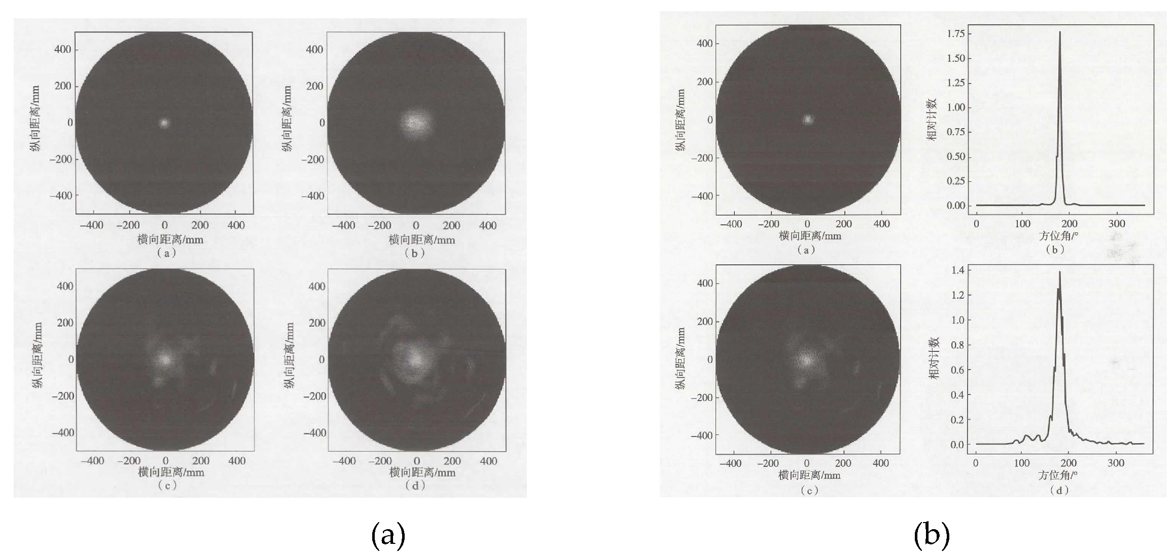
Researchers developed 3D CZT detection system data acquisition software using LabVIEW software. This software featured three distinct panel interfaces, each corresponding to system configuration, real-time display, and file storage. The software underwent testing and adjustments to ensure its functionality and effectiveness.
In 2018, Young-su Kim et al. from the Korea Institute of Radiological and Medical Sciences [176] developed a Compton backscatter imaging detector to enhance the sensitivity of portable non-mechanical collimation detectors and achieve three-dimensional imaging. Using the ML-EM algorithm for Full Width at Half Maximum (FWHM) analysis of the reconstructed images, the detector demonstrated 3D imaging capabilities and the ability to penetrate several tens of centimeters deep into the object under examination.
In 2014, researchers led by Yufei Gu et al. [177,178] conducted research on Compton backscattering imaging (CBST) using an improved iterative reconstruction algorithm. Addressing the sensitivity of CBST image reconstruction to noise and error in measured values, they proposed a novel CBST reconstruction algorithm. This method involved the use of the augmented Lagrangian multiplier to decompose the optimization problem into two sub-problems with analytical solutions. By iteratively solving these sub-problems, the augmented Lagrangian function was minimized to achieve image reconstruction. Several iterations successfully implemented ray attenuation correction, resulting in high-quality images. The newly designed algorithm exhibits advantages in reconstruction quality and convergence speed, significantly reducing reconstruction time and memory usage without compromising image quality.
In 2018, Gao Ge et al. [179] constructed a physical model for a Compton γ camera based on a 3D position-sensitive cadmium zinc telluride detector using Geant4 software. Image reconstruction work was performed based on data obtained from Monte Carlo simulations. The researchers applied inversion reconstruction and the Maximum Likelihood Expectation Maximization (MLEM) algorithm for image reconstruction.
Additionally, in 2019, Wei Wang [180] simulated a dual-layer Compton imaging system composed of position-sensitive CZT crystals. Using a combined theoretical and simulation-based approach, they conducted theoretical research on several factors that cause scattering angle errors in this imaging system, affecting its angular resolution capabilities. The team calculated the range of scattering angle errors caused by various factors affecting angular resolution for photons of different energies, subsequently proposing an optimized design for the imaging system structure. They provided a rational estimation method for the scattering angle errors in Compton imaging systems.
Furthermore, in 2019, Zhangyong Song et al. [181], investigated a novel non-mechanical collimated Compton camera technology for cancer therapy devices. Their research confirmed that the spatial resolution of the detector is the primary factor influencing the quality of Compton camera imaging. They emphasized the need to select appropriate crystal unit sizes for the detector while balancing detection efficiency.
In 2021, Yu Zhang [182] developed a three-layer Compton camera with two distinct operational modes based on Maximum Likelihood Estimation (MLEM). These two modes leverage single and double Compton scatterings, thereby enhancing the system's detection efficiency while enabling simultaneous detection of γ sources of different energies. The system underwent simulation using Geant4 and Python software, culminating in the detection outcomes of single-point and multi-point sources for both single and double Compton scatterings, as illustrated in Figure 12:
Figure 10. (a) Single-point source imaging effect, (b) multi-point source imaging effect [182].
Preprints 94531 g010
The information provided suggests that by obtaining the position and deposited energy information of events in the detector, the simulated imaging system achieved an optimal angular resolution of approximately 6.5°. This system enables simultaneous imaging of sources with different energies through a single measurement. Compared to imaging methods relying solely on the principles of single scattering, the inherent detection efficiency of the system improved by 31.2% under similar conditions.
In summary, both domestic and international research in Compton detection and imaging techniques for CZT detectors primarily focus on algorithm optimization. The aim is to improve the accuracy of spatial reconstruction of radiation sources by iteratively combining and enhancing algorithms.

5. Conclusions

CdZnTe, as an outstanding semiconductor detector material, has been continuously esteemed and studied since its discovery. It has been fashioned into various detector configurations. Detectors with array-distributed crystal surfaces have significant importance and utility in the detection and discrimination of γ and X-rays. These detectors, particularly CZT arrays, hold immense promise in nuclear detection applications. Research on CZT array detectors enables the rapid acquisition of high-resolution information about detected objects.
In recent years, research on CZT array detectors has primarily focused on the following areas:
  • CZT Crystal Research: Enhancing crystal performance by improving semiconductor crystal fabrication methods, doping with trace elements, refining etching processes, or applying surface coatings.
  • Optimization of Array Detector Electronics: Improving detector readout circuit design, enhancing the performance of electronic components, and increasing detector response speed and energy resolution.
  • Design of Novel CZT Array Detectors: Developing and optimizing applications for CZT array detectors, especially in the detection of specific nuclear materials.
  • Enhancement of Array Detector Imaging Algorithms: Improving imaging algorithms to achieve better reconstruction results and generate improved 3D images.
CZT array detectors, as semiconductor detectors with significant potential applications, offer numerous areas for further research and optimization. Future work could focus on advancing semiconductor crystal performance, optimizing detector electronics and algorithms, improving detector design, and exploring various avenues for further advancement in CZT array detector technology.

References

  1. Arlt, R.; Brutscher, J.; Gunnink, R.; Ivanov, V.; Parnham, K.; Soldner, S.; Stein, J. Use of CdZnTe detectors in hand-held and portable isotope identifiers to detect illicit trafficking of nuclear material and radioactive sources. In Proceedings of the 2000 IEEE Nuclear Science Symposium. Conference Record (Cat. No. 00CH37149), 2000; pp. 4/18-14/23 vol. 11.
  2. Sordo, S.D.; Abbene, L.; Caroli, E.; Mancini, A.M.; Zappettini, A.; Ubertini, P. Progress in the Development of CdTe and CdZnTe Semiconductor Radiation Detectors for Astrophysical and Medical Applications. Sensors (Basel) 2009, 9, 3491–3526. [Google Scholar] [CrossRef]
  3. Liu, L. The photoelectrical properties of CdZnTe nuclear radiation detector. Xiamen University of Technology, 2022.
  4. Szeles, C. CdZnTe and CdTe materials for X-ray and gamma ray radiation detector applications. physica status solidi (b) 2004, 241, 783–790. [Google Scholar] [CrossRef]
  5. Li, X.; Chu, J.H.; Li, L.X.; Dai, N.; Zhang, F.J. Investigation of room temperature nuclear radiation CdZnTe pixel array detector. Journal of Optoelectronics Laser 2008, 19, 751–753. [Google Scholar]
  6. Handong, L. Growth and Defects of CdxZn1-xTe Single Crystals. Sichuan University, 2004.
  7. LYU, L.; Liu, J.; LI, G. Research on High-Precision mm-Level Thickness Measurement Technology Based on Cadmium Zinc Telluride Detector. Journal of Isotopes 2023, 36, 285–294. [Google Scholar] [CrossRef]
  8. Hongzhao, Z.; Mingzhe, S.; Haixia, L. Simulating Response to Gamma Ray of CdZnTe Detector with CAPture Electrode Using Geant4. Atomic Energy Science and Technology 2021, 55, 1098–1104. [Google Scholar]
  9. Eisen, Y. Current state-of-the-art industrial and research applications using room-temperature CdTe and CdZnTe solid state detectors. Nuclear Instruments and Methods in Physics Research Section A: Accelerators, Spectrometers, Detectors and Associated Equipment 1996, 380, 431–439. [Google Scholar] [CrossRef]
  10. Lihao, W. Study on the pivotal techniques of gamma spectrum measurement in complex intense radiation field. National University of Defense Technology, 2021.
  11. Haijun, X. Data Acquisition System of CZT Nuclear Detector Based on FPGA. Chongqing University, 2013.
  12. Burger, A.; Groza, M.; Cui, Y.L.; Roy, U.N.; Hillman, D.; Guo, M.; Li, L.X.; Wright, G.W.; James, R.B. Development of portable CdZnTe spectrometers for remote sensing of signatures from nuclear materials. In Proceedings of the NATO Advanced Research Workshop on Advanced Materials for Radiation Detectors and Sensors/Symposium on Superconductors held at the 2004 E-MRS Fall Meeting, Warsaw, POLAND, 2005, Sep 06-10, 2004; pp. 1586-1591.
  13. Fan, Y.; Tao, W.; Boru, Z. Research Progress on CdZnTe Crystal Growth for Room Temperature Radiation Detection Applications. Journal of Synthetic Crystals 2020, 49, 561–569. [Google Scholar]
  14. Wanqi, J. Progress of Bridgman Crystal Growth Technology. Journal of Synthetic Crystals 2012, 24–35. [Google Scholar]
  15. Doty, F.; Butler, J.; Schetzina, J.; Bowers, K. Properties of CdZnTe crystals grown by a high pressure Bridgman method. Journal of Vacuum Science & Technology B: Microelectronics and Nanometer Structures Processing, Measurement, and Phenomena 1992, 10, 1418–1422. [Google Scholar]
  16. Szeles, C. Advances in the crystal growth and device fabrication technology of CdZnTe room temperature radiation detectors. IEEE Transactions on Nuclear Science 2004, 51, 1242–1249. [Google Scholar] [CrossRef]
  17. Szeles, C.; Cameron, S.E.; Ndap, J.O.; Chalmers, W.C. Advances in the crystal growth of semi-insulating CdZnTe for radiation detector applications. IEEE Transactions on Nuclear Science 2002, 49, 2535–2540. [Google Scholar] [CrossRef]
  18. Szeles, C.; Cameron, S.E.; Ndap, J.O.; Reed, M.D. Advances in the High-pressure Crystal Growth Technology of Semi-insulating CdZnTe for Radiation Detector Applications. Proceedings of SPIE - The International Society for Optical Engineering 2004, 5198. [Google Scholar]
  19. Szeles, C.; Cameron, S.E.; Soldner, S.A.; Ndap, J.O.; Reed, M.D. Development of the high-pressure electro-dynamic gradient crystal-growth technology for semi-insulating CdZnTe growth for radiation detector applications. Journal of Electronic Materials 2004, 33, 742–751. [Google Scholar] [CrossRef]
  20. Li, L.; Lu, F.; Lee, C.; Black, M.; Ouimette, D. New progress in large-size CZT (Zn=10%) single crystal growth using MVB technique for room temperature radiation detectors. IEEE 2004. [Google Scholar]
  21. Wang, T.; Jie, W.; Xu, Y.; Liu, W.; Zeng, D. Comparison between bottom-seeded Bridgman and accelerated crucible rotation Bridgman method for detector-grade CdZnTe growth. In Proceedings of the 2007 International Conference on Solid State Devices and Materials; 2007. [Google Scholar]
  22. Gangqiang, Z.; Tao, W.; Yadong, X. The development of CZT semiconductor X-ray and g-ray detectors. Physics 2013, 42, 862–869. [Google Scholar]
  23. Tao, W.; Yadong, X.; Gangqiang, Z. Detector Grade CdZnTe Crystal Growth and Device Fabrication. Mechanical Science and Technology for Aerospace Engineering 2010, 29, 546–550. [Google Scholar]
  24. Yang, F.; Jie, W.; Wang, M.; Sun, X.; Wang, T. Growth of Single-crystal Cd0.9Zn0.1Te Ingots using Pressure Controlled Bridgman Method. Crystals 2020, 10, 261. [Google Scholar] [CrossRef]
  25. Hermon, H.; Schieber, M.; Goorsky, M.; Lam, T.; Meerson, E.; Yao, H.; Erickson, J.; James, R.B. Characterization of CZT detectors grown from horizontal and vertical Bridgman. Proc Spie 2000, 186–193. [Google Scholar]
  26. A, I.J.; A, H.K.; B, A.B.; B, M.G.; B, M.G. Detailed studies of pixelated CZT detectors grown with the modified horizontal Bridgman method - ScienceDirect. Astroparticle Physics 2007, 28, 397–408. [Google Scholar]
  27. Wilson, M.D.; Cernik, R.; Chen, H.; Hansson, C.; Iniewski, K.; Jones, L.L.; Seller, P.; Veale, M.C. Small pixel CZT detector for hard X-ray spectroscopy. Nuclear Instruments and Methods in Physics Research Section A: Accelerators, Spectrometers, Detectors and Associated Equipment 2011, 652, 158–161. [Google Scholar] [CrossRef]
  28. Xi, C.; Tao, W.; Boru, Z.; Jie, H.; Yang, L.; Fan, Y.; Yadong, X.; Cangqiang, Z.; Wanqi, J. Study on Composition and Defects Uniformity of CdZnTe Crystal Grown by Travelling Heater Method. Journal of Synthetic Crystals 2013, 42, 2215–2229. [Google Scholar]
  29. Soldner, S.A.; Narvett, A.J.; Covalt, D.E.; Szeles, C. Characterization of the charge transport uniformity of CdZnTe crystals for large-volume nuclear detector applications. Ieee Transactions on Nuclear Science 2004, 51, 2443–2447. [Google Scholar] [CrossRef]
  30. Mackenzie, J.; Chen, H.; Awadalla, S.A.; Marthandam, P.; Redden, R.; Bindley, G.; He, Z.; Black, D.R.; Duff, M.; Amman, M. recent advances in thm czt for nuclear radiation detection introduction.
  31. Changhe, Z. Study on defect evaluation and VGF growth technique of CdZnTe materials. University of Chinese Academy of Sciences, 2021.
  32. Chu, M.; Terterian, S.; Ting, D.; Wang, C.; Benson, J.; Dinan, J.; James, R.; Burger, A. Effects of excess tellurium on the properties of CdZnTe radiation detectors. Journal of electronic materials 2003, 32, 778–782. [Google Scholar] [CrossRef]
  33. Nan, R.-h.; Jie, W.-q.; Zha, G.-q.; BAI, X.-x.; Bei, W.; Hui, Y. Determination of trap levels in CZT: In by thermally stimulated current spectroscopy. Transactions of Nonferrous Metals Society of China 2012, 22, s148–s152. [Google Scholar] [CrossRef]
  34. Roy, U.N.; Bolotnikov, A.E.; Camarda, G.S.; Cui, Y.; Hossain, A.; Lee, K.; Lee, W.; Tappero, R.; Yang, G.; Gul, R.; et al. High compositional homogeneity of CdTexSe1-x crystals grown by the Bridgman method. Apl Materials 2015, 3. [Google Scholar] [CrossRef]
  35. Roy, U.N.; Camarda, G.S.; Cui, Y.; Gul, R.; Yang, G.; Zazvorka, J.; Dedic, V.; Franc, J.; James, R.B. Evaluation of CdZnTeSe as a high-quality gamma-ray spectroscopic material with better compositional homogeneity and reduced defects. Sci Rep 2019, 9, 7303. [Google Scholar] [CrossRef] [PubMed]
  36. Roy, U.N.; Bolotnikov, A.E.; Camarda, G.S.; Cui, Y.; Hossain, A.; Lee, K.; Marshall, M.; Yang, G.; James, R.B. Growth of CdTexSe1-x from a Te-rich solution for applications in radiation detection. Journal of Crystal Growth 2014, 386, 43–46. [Google Scholar] [CrossRef]
  37. Nan, R.; Li, T.; Xu, G.; Jian, Z.; Li, X. Distribution of microscopic defects in Al-doped CdZnTe crystal. Journal of Materials Science 2017, 53, 4387–4394. [Google Scholar] [CrossRef]
  38. Yuan, W.; Zhang, C.; Liang, H.; Wang, X.; Shangguan, M.; Gong, Y.; Zhang, B.; Zhang, H.; Xie, H.; Yan, B. Investigating the influence of CdZnTe and HgCdTe material quality on detector image performance. Journal of Materials Science: Materials in Electronics 2021, 32, 13177–13186. [Google Scholar] [CrossRef]
  39. Chen, H.; Chattopadhyay, K.; Chen, K.-T.; Burger, A.; George, M.; Gregory, J.; Nag, P.; Weimer, J.; James, R. Passivation of CdZnTe surfaces by oxidation in low energy atomic oxygen. Journal of Vacuum Science & Technology A: Vacuum, Surfaces, and Films 1999, 17, 97–101. [Google Scholar]
  40. Dongmin, Z.; Shifu, Z.; Beijum, Z.; Deyou, G.; Jun, C.; Shihong, T.; Jun, F.; Xi, C. Surface Passivation Process of the Wafers for CdZnTe Detector. Journal of Synthetic Crystals 2006, 35, 715–718. [Google Scholar]
  41. Yubao, S.; Li, F.; Jie, R.; Gangqiang, C. Atomic oxygen exposure process on CdZnTe pixel detector suface. Journal of Functional Materials and Devices 2010, 16, 515–518. [Google Scholar]
  42. Hossain, A.; Bolotnikov, A.; Camarda, G.; Cui, Y.; Jones, D.; Hall, J.; Kim, K.; Mwathi, J.; Tong, X.; Yang, G. Novel approach to surface processing for improving the efficiency of CdZnTe detectors. Journal of electronic materials 2014, 43, 2771–2777. [Google Scholar] [CrossRef]
  43. Congfeng, L.; Shiwen, S.; Hualian, X. Effect of ampoule coating technology on defects in CdZnTe crystal. In Proceedings of the Photonics and optoelectronics Meetings; 2009. [Google Scholar]
  44. Lezhen, Z.; Zhenyu, Z.; Dong, W.; Guanghong, X.; Peili, G.; Fanning, M.; Zifeng, Z. CMP Parameter Optimization and Polishing Mechanism Analysis of Cadmium Zinc Telluride Wafer Based on the Orthogonal Test. Lubrication Engineering 2022, 47, 92–101. [Google Scholar]
  45. Peli, G. Preparation of Novel Abrasives and their applications in Chemical Mechanical Polishing for Cadmium Zinc Telluride Substrates. 2021. [Google Scholar] [CrossRef]
  46. Jian, J. Study of CdZnTe Pixel Arrays Nuclear Detector. Chongqing University, 2012.
  47. Mayer, M.; Hamel, L.A.; Tousignant, O.; Macri, J.R.; Ryan, J.M.; Mcconnell, M.L.; Jordanov, V.T.; Butler, J.F.; Lingren, C.L. Signal formation in a CdZnTe imaging detector with coplanar pixel and control electrodes. Nuclear Instruments & Methods in Physics Research 1999, 422, 190–194. [Google Scholar]
  48. Beilicke, M.; De Geronimo, G.; Dowkontt, P.; Garson, A.; Guo, Q.; Lee, K.; Martin, J.; Krawczynski, H. Performance of pixelated CZT detectors as a function of pixel and steering grid layout. Nuclear Instruments and Methods in Physics Research Section A: Accelerators, Spectrometers, Detectors and Associated Equipment 2013, 708, 88–100. [Google Scholar] [CrossRef]
  49. Abbene, L.; Del Sordo, S.; Caroli, E.; Gerardi, G.; Raso, G.; Caccia, S.; Bertuccio, G. Hard x-ray response of pixellated CdZnTe detectors. Journal of Applied Physics 2009, 105. [Google Scholar] [CrossRef]
  50. Xi, W.; Shali, X.; Miao, L.; Liuqian, Z.; Yulin, C.; Yuxiao, C. Further polarization effect of CdZnTe detectors under high flux X-ray irradiation. High Power Laser and Particle Beams 2013, 25, 773–777. [Google Scholar]
  51. Teague, L.C.; Washington, A.L.; Duff, M.C.; Groza, M.; Buliga, V.; Burger, A. Photo-induced currents in CdZnTe crystals as a function of illumination wavelength. Journal of Physics D-Applied Physics 2012, 45. [Google Scholar] [CrossRef]
  52. Dědič, V.; Franc, J.; Rejhon, M.; Grill, R.; Zázvorka, J.; Sellin, P. De-polarization of a CdZnTe radiation detector by pulsed infrared light. Applied Physics Letters 2015, 107. [Google Scholar] [CrossRef]
  53. Wangerin, K.; Du, Y.F.; Jansen, F. CZT performance for different anode pixel geometries and data corrections. Nuclear Instruments & Methods in Physics Research Section a-Accelerators Spectrometers Detectors and Associated Equipment 2011, 648, S37–S41. [Google Scholar] [CrossRef]
  54. Takahashi, T.; Watanabe, S. Recent progress in CdTe and CdZnTe detectors. IEEE Transactions on nuclear science 2001, 48, 950–959. [Google Scholar] [CrossRef]
  55. Bolotnikov, A.E.; Camarda, G.S.; Cui, Y.; Hossain, A.; Yang, G.; Yao, H.W.; James, R.B. Internal Electric-Field-Lines Distribution in CdZnTe Detectors Measured Using X-Ray Mapping. IEEE Transactions on Nuclear Science 2009, 56, 791–794. [Google Scholar] [CrossRef]
  56. Huichao, X.; Peirong, G. Analysis of Noise and Resolution of Prototype CdZnTe Detector. Nuclear Electronics & Detection Technology 2014, 34, 784–787. [Google Scholar]
  57. Bolotnikov, A.E.; Camarda, G.S.; Cui, Y.; Yang, G.; Hossain, A.; Kim, K.; James, R.B. Characterization and evaluation of extended defects in CZT crystals for gamma-ray detectors. Journal of Crystal Growth 2013, 379, 46–56. [Google Scholar] [CrossRef]
  58. Chuang, W.; Gangqiang, Z.; Yang, Q.; Rongrong, G.; Guangqi, W.; Wanqi, J. Fabrication and Characterization of CdZnTe Pixel Detector. Atomic Energy Science and Technology 2015, 49, 1320–1324. [Google Scholar]
  59. Lei, F.; Liangzhou, Z.; Xianglei, C.; Jie, W.; Yulin, Z. Study on Neutron Detection Performance of CdZnTe Detector. Nuclear Electronics & Detection Technology 2019, 39, 463–467. [Google Scholar]
  60. Yan, X.; Gao, X.; Sun, H.; Yang, D.; Zeng, T.; Luo, X.; Zhu, X.; Wangyang, P. Effect of surface treatment on photo-electric properties of CZT thick film for radiation detector. Materials science in semiconductor processing 2022, 148. [Google Scholar] [CrossRef]
  61. Min, S.; Shali, X.; Liuqiang, Z.; Yulin, C.; Yuxiao, C. Experiment and simulation of performance characteristics for pixellated CdZnTe detectors with various thickness. High Power Laser and Particle Beams 2014, 26, 210–215. [Google Scholar]
  62. Hui, Y.; Mengmeng, Z.; Yuanyuan, D.; Shouzhi, X.; Gangqiang, Z.; Wanqi, J. Analysis on Energy Spectra for CdZnTe Gamma Ray Detector. Journal of Synthetic Crystals 2021, 50, 1883–1891. [Google Scholar]
  63. Wanqi, J. Researches on the Preparation and Applications of CZT for X-ray and Gamma-ray Detectors. Materials China 2012, 815–823. [Google Scholar]
  64. Wanqi, J. Progress in Theories and Technologies of Crystal Growth of Ⅱ-Ⅵ Compounds. China Basic Science 2001, 15–19. [Google Scholar]
  65. Glasser, F.; Gerbe, V.; Ouvrier-Buffet, P.; Accensi, M.; Girard, J.; Renaud, M.; Gersten-Mayer, J. CdZnTe high-energy radiography detector. Nuclear Instruments and Methods in Physics Research Section A: Accelerators, Spectrometers, Detectors and Associated Equipment 2001, 458, 544–550. [Google Scholar] [CrossRef]
  66. Höschl, P.; Ivanov, Y.M.; Belas, E.; Franc, J.; Toth, A.L. Electrical and luminescence properties of (CdZn)Te single crystals prepared by the vertical gradient freezing method. Journal of Crystal Growth 1998, s 184–185, 1039-1043.
  67. J.E; Toney; and; B.A; Brunett; and; T.E; Schlesinger; and; J.M. Uniformity of Cd1 − xZnxTe grown by high-pressure Bridgman. Nuclear Instruments & Methods in Physics Research 1996.
  68. Li, Z.-F.; Lu, W.; Huang, G.; Yang, J.; He, L.; Shen, S. Microphotoluminescence mapping on CdZnTe: Zn distribution. Journal of Applied Physics 2001, 90, 260–264. [Google Scholar] [CrossRef]
  69. Polichar, R.; Schirato, R.; Reed, J. Development of CdZnTe energy selective arrays for industrial and medical radiation imaging. Nuclear Instruments and Methods in Physics Research Section A Accelerators Spectrometers Detectors and Associated Equipment 1994, 353, 349–355. [Google Scholar] [CrossRef]
  70. Tobin, S.; Tower, J.; Norton, P.; Chandler-Horowitz, D.; Amirtharaj, P.M.; Lopes, V.; Duncan, W.; Syllaios, A.; Ard, C.; Giles, N. A comparison of techniques for nondestructive composition measurements in CdZnTe substrates. Journal of electronic materials 1995, 24, 697–705. [Google Scholar] [CrossRef]
  71. Y. ; F.; Chen; C.; S.; Tsai; Y.; H.; Chang; Y. Hydrogen passivation in Cd1xZnxTe studied by photoluminescence. Applied Physics Letters 1991, 58, 493–493. [Google Scholar] [CrossRef]
  72. Xi, W. Principle and Experimental Characteristics of Pixellated CdZnTe Detector for Nuclear Radiation. Chongqing University, 2013.
  73. Krsmanovic, N.; Lynn, K.G.; Weber, M.H.; Tjossem, R.; Glass, H.L. Electrical compensation in CdTe and CdZnTe by intrinsic defects. Phys.rev.b 2000, 4141. [Google Scholar]
  74. Guo, R.; Jie, W.; Xu, Y.; Zha, G.; Wang, T.; Lin, Y.; Zhang, M.; Du, Z. Space-charge manipulation under sub-bandgap illumination in detector-grade CdZnTe. Journal of Electronic Materials 2015, 44, 3229–3235. [Google Scholar] [CrossRef]
  75. Xiang, C.; Kan, Z.; Shuai, H.; Kai, Z.; Hetong, H.; Long, H. Improvement on γ-ray Sensitivity of Current-mode CdZnTe Detector. Atomic Energy Science and Technology 2022, 56, 387–393. [Google Scholar]
  76. Yaxu, G. Performance non-uniformity of CdZnTe nuclear radiation detectors. Northwestern Polytechnical University, 2017.
  77. Xiaping, C. Research and Fabrication of 4H-SiC Ultraviolet p-i-n Photodiodes and Linear Array. Xiamen University, 2007.
  78. Abbene, L.; Del Sordo, S.; Fauci, F.; Gerardi, G.; La Manna, A.; Raso, G.; Cola, A.; Perillo, E.; Raulo, A.; Gostilo, V.; et al. Spectroscopic response of a CdZnTe multiple electrode detector. Nuclear Instruments and Methods in Physics Research Section A: Accelerators, Spectrometers, Detectors and Associated Equipment 2007, 583, 324–331. [Google Scholar] [CrossRef]
  79. Chengjie, F. Performance comparison of CdZnTe radiation detectors with PIN and MSM structure and the Study on leakage current of CdZnTe. SHANGHAI UNIVERSITY, 2022.
  80. Mitra; P. Current to Conductors Induced by a Moving Point Charge. American Journal of Physics 1970, 38, 112–112. [Google Scholar] [CrossRef]
  81. Ramot, S.R.E. currents induced by electron motion*. [CrossRef]
  82. Weifeng, Z.; Jinjie, W.; Xianqiang, T.; Rui, Z.; Pingzhou, L.; Bingbing, Q.; Mengyu, L.; Feng, Q. Simulation of energy spectrum characteristics of planar CdZnTe detector. Nuclear Techniques 2023, 46, 62–68. [Google Scholar]
  83. Montémont, G.; Argues, M.; Verger, L.; Rustique, J. A capacitive Frisch grid structure for CdZnTe detectors. In Proceedings of the 2000 IEEE Nuclear Science Symposium. Conference Record (Cat. No. 00CH37149); 2000; pp. 4/9–412. [Google Scholar]
  84. Luke, P.; Amman, M.; Lee, J.; Ludewigt, B.; Yaver, H. A CdZnTe coplanar-grid detector array for environmental remediation. Nuclear Instruments and Methods in Physics Research Section A: Accelerators, Spectrometers, Detectors and Associated Equipment 2001, 458, 319–324. [Google Scholar] [CrossRef]
  85. Bennett, P.R.; Shah, K.S.; Klugerman, M.; Squillante, M.R. High efficiency pixellated CdTe detector. Nuclear Instruments & Methods in Physics Research 1997, 392, 260–263. [Google Scholar]
  86. Bale, D.S.; Franks, L.A.; Szeles, C.; Burger, A.; James, R.B.; Barber, H.B.; Doty, F.P.; Roehrig, H. Design of high-performance CdZnTe quasi-hemispherical gamma-ray CAPture plus detectors. In Proceedings of the Hard X-Ray and Gamma-Ray Detector Physics and Penetrating Radiation Systems VIII; 2006. [Google Scholar]
  87. Zhu, Y.; He, Z. Performance of Larger-Volume 40× 40× 10-and 40× 40× 15-mm³ CdZnTe Detectors. IEEE Transactions on Nuclear Science 2021, 68, 250–255. [Google Scholar] [CrossRef]
  88. Veale, M.C.; Bell, S.J.; Jones, L.L.; Seller, P.; Wilson, M.D.; Allwork, C.; Kitou, D.; Sellin, P.J.; Veeramani, P.; Cernik, R.C. An ASIC for the Study of Charge Sharing Effects in Small Pixel CdZnTe X-Ray Detectors. IEEE Transactions on Nuclear Science 2011, 58, 2357–2362. [Google Scholar] [CrossRef]
  89. Brunett, B.A.; Van Scyoc, J.M.; James, R.B.; Schlesinger, T.E. CdZnTe pixel array detectors and implications for producing large volume gamma-ray spectrometers. Journal of Applied Physics 1999, 86, 3926–3933. [Google Scholar] [CrossRef]
  90. Jun, W.; Xiaopan, J.; Zhiming, Z.; Chao, W.; Yu, X.; Yan, L.; Guoqiang, Z. Research on depth sensitivity and energy correction technology based on pixel CZT detector. Computing Techniques for Geophysical and Geochemical Exploration 2020, 42, 401–406. [Google Scholar]
  91. Jun, W. Study and Test of Energy Spectrum Reading of Pixel and Hemispherical Cadmium Zinc Telluride Detectors. Chengdu University of Technology, 2020.
  92. Zheng, W. Design of Electronics Readout System for Multilayer Array of CZT Detectors. North China Electric Power University, 2020.
  93. Bolotnikov, A.E.; Camarda, G.C.; Wright, G.W.; James, R.B. Factors limiting the performance of CdZnTe detectors. IEEE Transactions on Nuclear Science 2005, 52, 589–598. [Google Scholar] [CrossRef]
  94. Bolotnikov, A.E.; Butcher, J.; Camarda, G.S.; Cui, Y.; De Geronimo, G.; Fried, J.; Gul, R.; Fochuk, P.M.; Hamade, M.; Hossain, A.; et al. Array of Virtual Frisch-Grid CZT Detectors With Common Cathode Readout for Correcting Charge Signals and Rejection of Incomplete Charge-Collection Events. IEEE Transactions on Nuclear Science 2012, 59, 1544–1551. [Google Scholar] [CrossRef]
  95. Li, Q.; Beilicke, M.; Lee, K.; Garson Iii, A.; Guo, Q.; Martin, J.; Yin, Y.; Dowkontt, P.; De Geronimo, G.; Jung, I. Study of thick CZT detectors for X-ray and Gamma-ray astronomy. Astroparticle Physics 2011, 34, 769–777. [Google Scholar] [CrossRef]
  96. Wilson, M.D.; Seller, P.; Veale, M.C.; Sellin, P.J. Investigation of the small pixel effect in CdZnTe detectors. In Proceedings of the 2007 IEEE Nuclear Science Symposium Conference Record; 2007; pp. 1255–1259. [Google Scholar]
  97. Jianl, J.; Shalil, X.; Xin, C.; Liuqian, Z.; Yuxia, C.; Yulin, C. Noise Analysis of Array Pixellated CZT Detector. Optoelectronic Technology 2011, 31, 98–102. [Google Scholar]
  98. Wei, W.; Dingdong, Z.; U-Fat, C.; Bowen, L.; Shan, Z.; Deyu, X.; Miao, L. A High Speed Front End Readout Circuit for CdZnTe Detectors. Microelectronics 2022, 52, 376–382. [Google Scholar] [CrossRef]
  99. Bolotnikov, A.E.; Cook, W.R.; Harrison, F.A.; Wong, A.S.; Schindler, S.M.; Eichelberger, A.C. Charge loss between contacts of CdZnTe pixel detectors. Nuclear Instruments & Methods in Physics Research 1999, 432, 326–331. [Google Scholar]
  100. Bolotnikov, A.E. Optimization of virtual Frisch-grid CdZnTe detector designs for imaging and spectroscopy of gamma rays. Proceedings of SPIE - The International Society for Optical Engineering 2007, 6706. [Google Scholar]
  101. Iniewski, K.; Chen, H.; Bindley, G.; Kuvvetli, I.; Budtz-Jorgensen, C. Modeling charge-sharing effects in pixellated CZT detectors. In Proceedings of the 2007 IEEE Nuclear Science Symposium Conference Record; 2007; pp. 4608–4611. [Google Scholar]
  102. Yin, Y.; Komarov, S.; Wu, H.; Song, T.Y.; Li, Q.; Garson, A.; Lee, K.; Simburger, G.; Dowkontt, P.; Krawczynski, H. Characterization of highly pixelated CZT detectors for sub-millimeter PET imaging. In Proceedings of the 2009 IEEE Nuclear Science Symposium Conference Record (NSS/MIC); 2009; pp. 2411–2414. [Google Scholar]
  103. James, R.B.; Chen, H.; Burger, A.; Awadalla, S.A.; Iniewski, K.; Franks, L.A.; Lu, P.H.; Harris, F.; Mackenzie, J.; Hasanen, T.; et al. Large-volume high-resolution cadmium zinc telluride radiation detectors: recent developments. In Proceedings of the Hard X-Ray and Gamma-Ray Detector Physics IX; 2007. [Google Scholar]
  104. Kim, J.C.; Anderson, S.E.; Kaye, W.; Zhang, F.; Zhu, Y.; Kaye, S.J.; He, Z. Charge sharing in common-grid pixelated CdZnTe detectors. Nuclear Instruments and Methods in Physics Research Section A: Accelerators, Spectrometers, Detectors and Associated Equipment 2011, 654, 233–243. [Google Scholar] [CrossRef]
  105. Zurum, X. The imaging detector arrays for X and γ rays. Nuclear Electronics & Detection Technology 2000, 20, 62–65. [Google Scholar]
  106. Jie, Y.; Huiping, G.; Rusong, L. The Currency and Development of X or γ Detector Arrays. 2006, 265-268. doi:ConferenceArticle/5aa2814ac095d72220a38ddd.
  107. Hong, J.; Allen, B.; Grindlay, J.; Chammas, N.; Barthelemy, S.; Baker, R.; Gehrels, N.; Nelson, K.E.; Labov, S.; Collins, J.; et al. Building large area CZT imaging detectors for a wide-field hard X-ray telescope—ProtoEXIST1. Nuclear Instruments and Methods in Physics Research Section A: Accelerators, Spectrometers, Detectors and Associated Equipment 2009, 605, 364–373. [Google Scholar] [CrossRef]
  108. Grindlay, J.; Hong, J.; Allen, B.; Barthelmy, S.; Baker, R. Development of tiled imaging CZT detectors for sensitive wide-field hard X-ray surveys to EXIST. Nuclear Instruments and Methods in Physics Research Section A: Accelerators, Spectrometers, Detectors and Associated Equipment 2011, 652, 671–673. [Google Scholar] [CrossRef]
  109. Zhang, F.; Herman, C.; He, Z.; De Geronimo, G.; Vernon, E.; Fried, J. Characterization of the H3D ASIC Readout System and 6.0 cm 3-D Position Sensitive CdZnTe Detectors. Nuclear Science, IEEE Transactions on 2012, 59, 236–242. [Google Scholar] [CrossRef]
  110. Yin, Y.; Chen, X.; Wu, H.; Komarov, S.; Garson, A.; Li, Q.; Guo, Q.; Krawczynski, H.; Meng, L.-J.; Tai, Y.-C. 3-D spatial resolution of 350/spl mu/m pitch pixelated CdZnTe detectors for imaging applications. IEEE transactions on nuclear science 2012, 60, 9–15. [Google Scholar] [CrossRef]
  111. Yin, Y.; Chen, X.; Komarov, S.; Wu, H.; Wen, J.; Krawczynski, H.; Meng, L.-J.; Tai, Y.-C. Study of Highly Pixelated CdZnTe Detector for PET Applications. Physics Procedia 2012, 37, 1537–1545. [Google Scholar] [CrossRef]
  112. Chen; Xiang; He-Tong; Gang. Experimental study on high dose rate response of cadmium zinc telluride detectors to pulsed X-ray.
  113. Ukaegbu, I.K.; Gamage, K.A.A. A Model for Remote Depth Estimation of Buried Radioactive Wastes Using CdZnTe Detector. Sensors (Basel) 2018, 18. [Google Scholar] [CrossRef]
  114. Chao, P. Research on Key Technologies of Airborne Multi-beam Array Detection 3D Imaging Lidar. China Academy of Launch Vehicle Technology, 2022.
  115. He, Z.; Li, W.; Knoll, G.F.; Wehe, D.K.; Du, Y.F. Effects of charge sharing in 3-D position sensitive CdZnTe gamma-ray spectrometers. Nuclear Instruments and Methods in Physics Research Section A: Accelerators, Spectrometers, Detectors and Associated Equipment 2000, 439, 619–624. [Google Scholar] [CrossRef]
  116. He, Z.; Knoll, G.F.; Wehe, D.K.; Rojeski, R.; Mastrangelo, C.H.; Hammig, M.; Barrett, C.; Uritani, A. 1-D position sensitive single carrier semiconductor detectors. Nuclear Instruments & Methods in Physics Research 1996, 380, 228–231. [Google Scholar]
  117. Li, W.; He, Z.; Knoll, G.F.; Wehe, D.K.; Du, Y.F. A modeling method to calibrate the interaction depth in 3-D position sensitive CdZnTe gamma-ray spectrometers. In Proceedings of the 1999 IEEE Nuclear Science Symposium. Conference Record. 1999 Nuclear Science Symposium and Medical Imaging Conference (Cat. No.99CH37019); 2002. [Google Scholar]
  118. Liptac, J.; Parker, R.; Tang, V.; Peysson, Y.; Decker, J. Hard x-ray diagnostic for lower hybrid experiments on Alcator C-Mod. Review of Scientific Instruments 2006, 77, 3987. [Google Scholar] [CrossRef]
  119. Vernon, E.; Ackley, K.; De Geronimo, G.; Fried, J.; He, Z.; Herman, C.; Zhang, F. ASIC for High Rate 3D Position Sensitive Detectors. IEEE Transactions on Nuclear Science 2010, 57, 1536–1542. [Google Scholar] [CrossRef]
  120. Lee, Y. Improved quality using newly designed algorithms in gamma- and X-ray fusion images with a photon counting CZT detector: Combining the median modified Wiener filter and edge detection method. Optik 2021, 245. [Google Scholar] [CrossRef]
  121. Li, Y.; Gong, P.; Tang, X.; Hu, Z.; Wang, P.; Tian, F.; Wu, S.; Ye, M.; Zhou, C.; Zhu, X. DOI correction for gamma ray energy reconstruction based on energy segment in 3D position-sensitive CdZnTe detectors. Journal of Instrumentation 2022, 17, T03004-. [Google Scholar] [CrossRef]
  122. Lianjun, Z.; Siya, X.; Yulai, Z.; Yong, L.; Chao, L.; Qiang, W. Monte Carlo Simulation Study of A Large Area Array Neutron Gamma Discrimination Detector. Journal of Isotopes 2022, 35, 460–467. [Google Scholar]
  123. Zhanjun, X.; Yon, M.; Xiangdon, R.; Guoqin, Z.; Weiming, W. Simulation calculation of gamma-ray spectrum in CZT detector based on Monte Carlo method. Nuclear Electronics & Detection Technology 2008, 28, 52–55. [Google Scholar]
  124. Kuan, S.; Ywfang, C.; Liming, D. Study on Self-adapting Processing Method in Radiant Image. Nuclear Electronics & Detection Technology 2009, 29, 517–520. [Google Scholar]
  125. Fayuan, X.; Fengjun, S. Fabrication and γ spectrum characteristic test of a laminated CdZnTe detector. High Power Laser and Particle Beams 2018, 30, 163–167. [Google Scholar]
  126. Bolotnikov, A.E.; Boggs, S.E.; Hubert, C.M.; Cook, W.R.; Schindler, S.M. Investigation of optimal contact geometries for CdZnTe pixel detectors. In Proceedings of the Conference on hard x-ray, gamma-ray, and neutron detector physics; 2000. [Google Scholar]
  127. Bolotnikov, A.E.; Boggs, S.E.; Chen, C.M.H.; Cook, W.R.; Schindler, S.M. Properties of Pt Schottky Type Contacts On High-Resistivity CdZnTe Detectors. Nuclear Instruments and Methods in Physics Research Section A Accelerators Spectrometers Detectors and Associated Equipment 2001, 482, 395–407. [Google Scholar] [CrossRef]
  128. Sang, W.; Wei, J.; Qi, Z.; Wanwan, L.; Jiahua, M.; Jianyong, T.; Yongbiao, Q. Primary study on the contact degradation mechanism of CdZnTe detectors. Nuclear Instruments and Methods in Physics Research Section A: Accelerators, Spectrometers, Detectors and Associated Equipment 2004, 527, 487–492. [Google Scholar] [CrossRef]
  129. Xiaoyan, L.; Jiahua, M.; Yue, Z.; Changjun, W.; Wenbin, S.; Kaifeng, Q.; Dongni, H.; Chenying, Z. Property comparisons of Au-CZT and Au/Cr-CZT contacts. Journal of Functional Materials and Devices 2010, 16, 1–5. [Google Scholar]
  130. Roy, U.N.; Mundle, R.M.; Camarda, G.S.; Cui, Y.; Gul, R.; Hossain, A.; Yang, G.; Pradhan, A.K.; James, R.B. Novel ZnO:Al contacts to CdZnTe for X- and gamma-ray detectors. Rep 2016, 6, 26384. [Google Scholar] [CrossRef] [PubMed]
  131. Ling, L.; Zhang, J.; Zhao, S.; Zhang, D.; Zhang, J.; Shi, H.; Tang, K.; Liang, X.; Huang, J.; Min, J.; et al. Surface analysis and electrical measurement of the ohmic contact on p-CdZnTe (111)B face with Au/Cd composite electrode. Materials Science in Semiconductor Processing 2019, 98, 90–94. [Google Scholar] [CrossRef]
  132. Benjie, Z. Research on Signal Readout Circuit Based on CdZnTe Pixel-lated Radiation Detector. Chongqing University of Posts and Telecommunications, 2019.
  133. Yinsong, P.; Fenglin, L.; Shuaiju, Y. Design on readout circuit of CZT pixel nuclear radiation detector. Transducer and Microsystem Technologies 2012, 31, 125–127. [Google Scholar] [CrossRef]
  134. Xiangquan, L. Study of A Readout Circuit for CZT Surface Element Pixel Arrays Nuclear Radiation Detector. Chongqing University, 2010.
  135. Xin, C. Study of CZT Pixel Arrays Nuclear Detector and Design of Electronics. Chongqing University, 2011.
  136. Songmeng, F. Research on wavefront distortion compensation algorithm based on array detector. Xidian University, 2022.
  137. Gevin, O.; Baron, P.; Coppolani, X.; Delagnes, E.; Daly, F.; Limousin, O.; Lugiez, F.; Meuris, A.; Pinsard, F. IDeF-X ECLAIRs: An ultra low noise CMOS ASIC for the readout of Cd (Zn) Te detectors. In Proceedings of the 2007 IEEE Nuclear Science Symposium Conference Record; 2007; pp. 326–332. [Google Scholar]
  138. Gao, W.; Gan, B.; Li, X.; Wei, T.; Gao, D.; Hu, Y. Development of a compact radiation-hardened low-noise front-end readout ASIC for CZT-based hard X-ray imager. Nuclear Instruments & Methods in Physics Research Section a-Accelerators Spectrometers Detectors and Associated Equipment 2015, 780, 15–20. [Google Scholar] [CrossRef]
  139. Espagnet, R.; Frezza, A.; Martin, J.-P.; Hamel, L.-A.; Després, P. Conception and characterization of a virtual coplanar grid for a 11×11 pixelated CZT detector. Nuclear Instruments and Methods in Physics Research Section A: Accelerators, Spectrometers, Detectors and Associated Equipment 2017, 860, 62–69. [Google Scholar] [CrossRef]
  140. Kuihong, H.; Lin, Z.; Yongna, C.; Huaxian, W. 16-channel CdZnTe system for low-energy γ-ray measurement. Nuclear Techniques 2008, 31, 869–872. [Google Scholar]
  141. Kuihon, H.; Xiangguo, F.; Yongna, C.; Min, M.; Huaxian, W. Optimized design of Compton scattering collimators to array detectors of discriminate grade CdZnTe. Nuclear Techniques 200, 33, 793-796.
  142. Thrall, C.L.; Wahl, C.G.; He, Z. Performance of five-or-more-pixel event sequence reconstruction for 3-D semiconductor gamma-ray-imaging spectrometers. In Proceedings of the IEEE Nuclear Science Symposium Conference Record; 2009. [Google Scholar]
  143. Fenglin, L. A Study of A Readout Circuit Used for CZT Pixel Arrays Nuclear Radiation Detector. Chongqing University, 2012.
  144. Wei, L. Design of SAR-ADC Used for CZT Detector Imaging System. Northwestern Polytechnical University, 2017.
  145. Guo; Panjie; Liu; Wei; Tingcun; Yongcai; Bo. Design of a 12-bit 1 MS/s SAR-ADC for front-end readout of 32-channel CZT detector imaging syst em. Nuclear Instruments and Methods in Physics Research, Section A. Accelerators, Spectrometers, Detectors and Associated Equipment 2015.
  146. Liu, W.; Wei, T.; Li, B.; Yang, L.; Hu, Y. A reference voltage in capacitor–resister hybrid SAR ADC for front-end readout system of CZT detector. Journal of Semiconductors 2016, 37. [Google Scholar] [CrossRef]
  147. W.; Liu; T.; Wei; L.; Yang; Y.; Hu. A 12-bit, 1 MS/s SAR-ADC for a CZT-based multi-channel gamma-ray imager using a new digital calibration method. Journal of Instrumentation 2016, 11.
  148. Krummenacher, F. Pixel detectors with local intelligence: an IC designer point of view. Nuclear Instruments and Methods in Physics Research Section A: Accelerators, Spectrometers, Detectors and Associated Equipment 1991, 305, 527–532. [Google Scholar] [CrossRef]
  149. Xin, C.; Shali, X.; Liuqian, Z.; Yuxia, C.; Yulin, C.; Jian, J. Design of Pulse Shaped Circuit Based on CdZnTe Detector. Optoelectronic Technology 2010, 30. [Google Scholar]
  150. Xiaoru, Z.; Ningning, T.; Xiaowei, H.; Shanshan, D. A Fast Polar Format Imaging Algorithm of MIMO Radarwith Sparse Array Based on Two-dimensional CZT. Journal of Air Force Engineering University 2017, 18, 32–36. [Google Scholar]
  151. Meleshenkovskii, I.; Carrel, F.; Simon, A.C.; Espagnon, I. Isotopic Composition Determination Codes: Current State-of-the-Art, Recent Developments and Future Challenges. Journal of nuclear materials management 2021, 49. [Google Scholar]
  152. Goodman, D.; Streicher, M.; Zhu, Y.; Brown, S.; He, Z. 1-D Fast Neutron Source Localization Using Digital Pixelated 3-D Position-Sensitive CdZnTe Detectors. IEEE Transactions on Nuclear Science 2017, 64, 2531–2535. [Google Scholar] [CrossRef]
  153. Streicher, M.; Goodman, D.; Zhu, Y.; Brown, S.; Kiff, S.; He, Z. Fast neutron detection using pixelated CdZnTe spectrometers. IEEE Transactions on Nuclear Science 2017, 64, 1920–1926. [Google Scholar] [CrossRef]
  154. Streicher, M.; Brown, S.; Zhu, Y.; Goodman, D.; He, Z. Special nuclear material characterization using digital 3-D position sensitive CdZnTe detectors and high purity germanium spectrometers. IEEE Transactions on Nuclear Science 2016, 63, 2649–2656. [Google Scholar] [CrossRef]
  155. He, Z.; Whe, D.; Knoll, G. Development of Gamma-Ray Compton Imager Using Room-Temperature 3-D Position Sensitive Semiconductor Detectors. office of scientific & technical information technical reports 2003. [Google Scholar]
  156. Mortreau, P.; Berndt, R. Characterisation of cadmium zinc telluride detector spectra–application to the analysis of spent fuel spectra. Nuclear Instruments and Methods in Physics Research Section A: Accelerators, Spectrometers, Detectors and Associated Equipment 2001, 458, 183–188. [Google Scholar] [CrossRef]
  157. Bolotnikov, A.E.; James, R.B.; Cui, Y.; De Geronimo, G.; Vernon, E.; Camarda, G.; Hossain, A.; Yang, G.; Indusi, J.; Boyer, B. High-Efficiency CdZnTe Position-Sensitive VFG Gamma-Ray Detectors for Safeguards Applications; Brookhaven National Lab.(BNL), Upton, NY (United States): 2015.
  158. Bolotnikov, A.E.; Camarda, G.S.; Chen, E.; Cheng, S.; Cui, Y.; Gul, R.; Gallagher, R.; Dedic, V.; De Geronimo, G.; Ocampo Giraldo, L. CdZnTe position-sensitive drift detectors with thicknesses up to 5 cm. Applied Physics Letters 2016, 108. [Google Scholar] [CrossRef]
  159. Bolotnikov, A.E.; Ackley, K.; Camarda, G.S.; Cui, Y.; Eger, J.F.; De Geronimo, G.; Finfrock, C.; Fried, J.; Hossain, A.; Lee, W. High-Efficiency CdZnTe Gamma-Ray Detectors. IEEE Transactions on Nuclear Science 2015, 62, 3193–3198. [Google Scholar] [CrossRef]
  160. Goodman, D.; Xia, J.; Sanders, J.; He, Z. FRAM v5. 2 estimation of plutonium and uranium isotopics using digitized 3-D position-sensitive CdZnTe detectors. Nuclear Instruments and Methods in Physics Research Section A: Accelerators, Spectrometers, Detectors and Associated Equipment 2020, 954, 161339. [Google Scholar] [CrossRef]
  161. Xuesong, L.; Jianzhong, N.; Gongshuo, Y.; Jianfeng, L.; Yonggang, Z.; Xiaolin, Z. Portable Anti-Compton γ Detection Systemsfor High Activity Source Measurement. Modern Applied Physics 2021, 12, 13–18. [Google Scholar]
  162. Parajuli, R.K.; Sakai, M.; Parajuli, R.; Tashiro, M. Development and Applications of Compton Camera—A Review. Sensors 2022, 22. [Google Scholar] [CrossRef]
  163. Chuanpeng, W.; Liang, L. Review of Compton camera imaging technology development. Nuclear Techniques 2021, 44, 45–56. [Google Scholar]
  164. Xiaojun, D. Research on reconstruction of radiation distribution based on γ camera images. China Academy of Engineering Physics, 2012.
  165. Yilin, L. Research on Compton imaging base on a 3-D position sensitive CdZnTe detector. Tsinghua University, 2018.
  166. Yang, Y.; Gono, Y.; Motomura, S.; Enomoto, S.; Yano, Y. A Compton camera for multitracer imaging. IEEE Transactions on Nuclear Science 2001, 48, 656–661. [Google Scholar] [CrossRef]
  167. Burger, A.; Zhang, F.; James, R.B.; He, Z.; Franks, L.A. 3D position-sensitive CdZnTe gamma-ray spectrometers: improved performance with new ASICs. In Proceedings of the Hard X-Ray and Gamma-Ray Detector Physics VI; 2004; pp. 135–143. [Google Scholar]
  168. De Geronimo, G.; Vernon, E.; Ackley, K.; Dragone, A.; Fried, J.; O'Connor, P.; He, Z.; Herman, C.; Zhang, F. Readout ASIC for 3D position-sensitive detectors. In Proceedings of the 2007 IEEE Nuclear Science Symposium Conference Record; 2007; pp. 32–41. [Google Scholar]
  169. Wang, W.; Wahl, C.G.; He, Z. Maximum likelihood estimation maximization deconvolution in spatial and combined spatial- energy domains for a detector array system. In Proceedings of the IEEE Nuclear Science Symposium Conference Record; 2007. [Google Scholar]
  170. Miao, L.; Shali, X.; Liuqiang, Z.; Yulin, C.; Yuxiao, C.; Min, S.; Xi, W. Gamma source imaging based on pixeilated CdZnTe detection. High Power Laser and Particle Beams 2010, 22, 2165–2170. [Google Scholar] [CrossRef]
  171. Xi, W.; Shali, X.; Liuqiang, Z.; Yuxiao, C.; Yulin, C.; Miao‚, L.; Min, S.; Xin, C.; Jian, J. Study of 2×2 pixellated nuclear radiation detector based on CdZnTe. Journal of Optoelectronics·Laser 2010, 21, 639–643. [Google Scholar] [CrossRef]
  172. Miao, L.; Shali, X.; Xi, W.; Yulin, C.; Yuxiao, C.; Ling, N.; Liuqiang, Z. Carrier-trapping-based imaging evaluation model and experiment of pixellated CdZnTe detector. High Power Laser and Particle Beams 2011, 23, 3405–3411. [Google Scholar] [CrossRef]
  173. Wang, X.; Xiao, S.; Li, M.; Zhang, L.; Chen, Y. Intensifying process of polarization ef fect within pixellated CdZnTe detectors for X-ray imaging. Chinese Optics Letters 2011, 9, 6–8. [Google Scholar] [CrossRef]
  174. Miao, L. Principle, System and Characteristics of Pixellated CdZnTe Detector for High Energy Radiation. 2012.
  175. Jianqiang, F. Research on the key techniques of CdZnTe Detector. Tsinghua University, 2017.
  176. Young-Su; Kim; Jae; Hyeon; Kim; Junyoung; Lee; Chan; Hyeong; Kim. Large-Area Compton Camera for High-Speed and 3-D Imaging. IEEE Transactions on Nuclear Science 2018.
  177. Yufei, G. Research on the Image Reconstruction Algorithms for Compton Back-scattering Tomography Based on Energy Spectrum. Information Engineering University, 2014.
  178. Yufei, G.; Bin, Y.; Lei, L.; Yu, H. Reviews of Image Reconstruction Algorithms in Compton Scattering Tomography. Computerized Tomography Theory and Applications 2013, 22, 553–562. [Google Scholar]
  179. Ge, G. Monte Carlo Simulation and Image Reconstruction of Compton Camera Based on Geant4. China Institute for Radiation Protection, 2018.
  180. Wei, W.; Chuanlong, L.; Jianhua, W.; Xinglong, L. Theoretical and Simulation Study on Factor Affecting Angular Resolution of Compton Imaging System. Atomic Energy Science and Technology 2019, 53, 2471–2477. [Google Scholar] [CrossRef]
  181. Song Zhangyong; Yu Deyang; Cai Xiaohong. Analysis and simultion for Compton camera′s imaging resolution. Acta Physica Sinica 2019, 68, 269–277. [CrossRef]
  182. Yu, Z.; Guoguang, Z. The Design and Simulation of a New Multilayer Compton Camera. Nuclear Electronics & Detection Technology 2021, 41, 1085–1092. [Google Scholar]
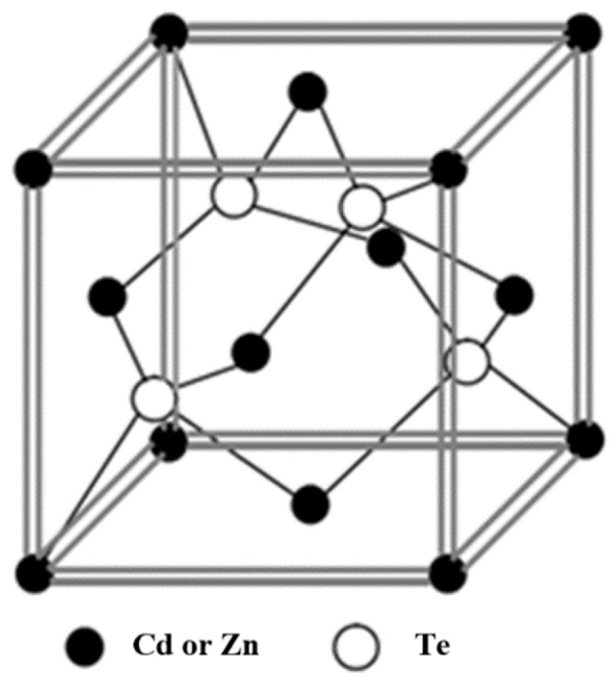
Figure 1. Lattice structure of CZT crystals.
Preprints 94531 g001
Figure 2. Schematic diagram of semiconductor photodetectors with different configurations.
Preprints 94531 g002
Figure 3. Schematic diagram of CZT detector surface configuration with different unipolar electrode structures.
Preprints 94531 g003
Figure 4. Schematic diagram of the working principle of CZT array detector [91].
Preprints 94531 g004
Figure 5. Anode design of pixelated CZT detector for non-collecting steering mesh model [104].
Preprints 94531 g005
Figure 6. Geant4 simulation calculation flowchart [123].
Preprints 94531 g006
Figure 7. Schematic diagram of the charge-sensitive preamplifier circuit [146].
Preprints 94531 g007
Figure 8. The principle of the proposed Compton camera.
Preprints 94531 g008
Figure 9. Block diagram of the data acquisition board principle design.
Preprints 94531 g009
Table 1. Comparison of the properties of different detector materials [9,10,11].
Material Atomic number Density (g/cm3) Bandgap width (eV) Ionization energy (eV) Resistivity μeτe μhτh
Si 14 2.33 1.12 3.62 104 >1 1
Ge 32 5.33 0.67 2.96 50 >1 >1
InP 15/49 4.78 1.35 4.2 106 5×10⁻⁶ <2×10⁻⁵
GaAs 33/31 5.32 1.43 4.2 107 10-5 10-6
HgI2 80/53 6.40 2.13 4.2 1013 10-4 10-5
PbI2 82/53 6.20 2.3~2.6 4.9 1012 10-6 10-7
TlBr 81/35 7.56 2.68 6.5 1012 10-5 10-6
CdTe 48/52 6.20 1.44 4.43 109 10-3 10-4
Cd0.9Zn0.1Te 48/30/52 5.78 1.57 4.64 1010~1011 10-3~10-2 10-5
Cd0.8Zn0.2Te 48/3052 6.02 1.5~2.2 5.0 1010~1011 10-3 10-6~10-5
Disclaimer/Publisher’s Note: The statements, opinions and data contained in all publications are solely those of the individual author(s) and contributor(s) and not of MDPI and/or the editor(s). MDPI and/or the editor(s) disclaim responsibility for any injury to people or property resulting from any ideas, methods, instructions or products referred to in the content.
Copyright: This open access article is published under a Creative Commons CC BY 4.0 license, which permit the free download, distribution, and reuse, provided that the author and preprint are cited in any reuse.
Prerpints.org logo

Preprints.org is a free preprint server supported by MDPI in Basel, Switzerland.

Subscribe

© 2024 MDPI (Basel, Switzerland) unless otherwise stated