Submitted:
27 December 2023
Posted:
27 December 2023
You are already at the latest version
Abstract
Keywords:
1. Introduction
2. Materials and Methods
2.1. Reagents and Materials
2.2. Adhesive Manufacture
2.3. Manufacture of the Functional Films
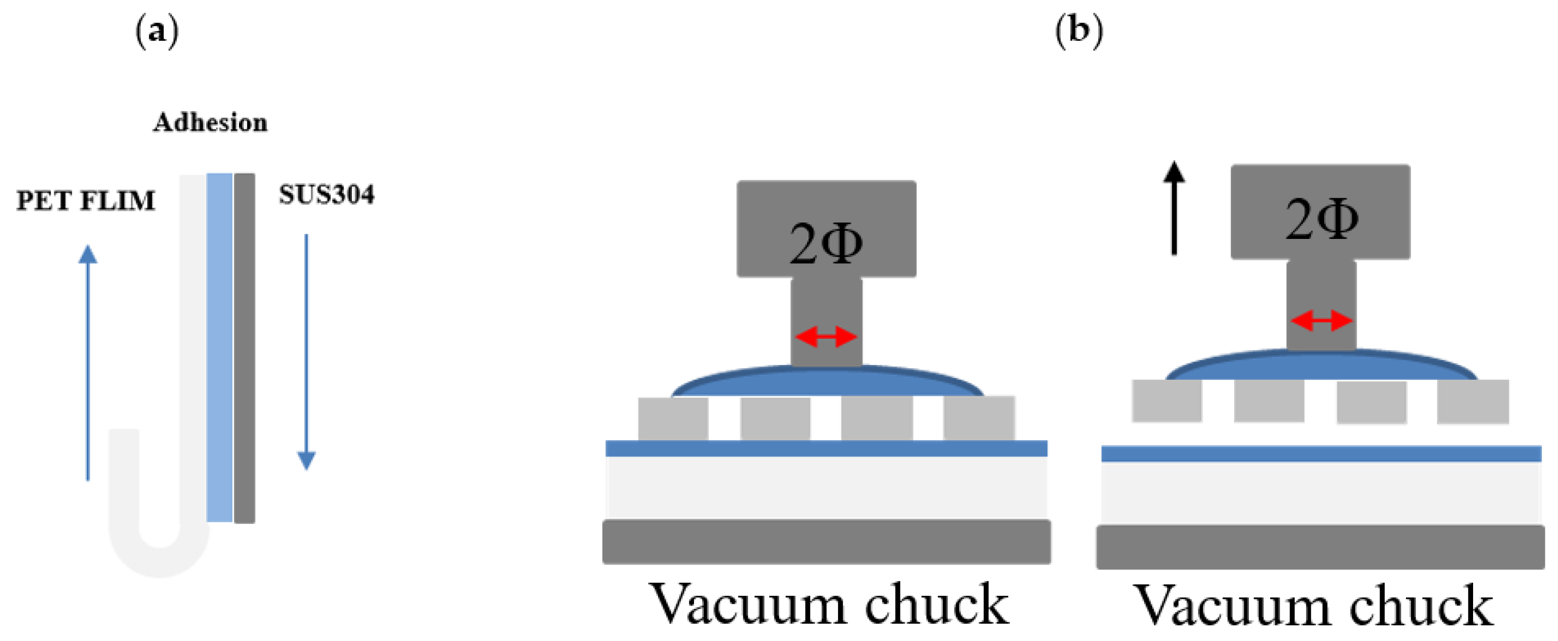
2.4. Measurement of Adhesion
2.5. Temperature Control
3. Results and Discussion
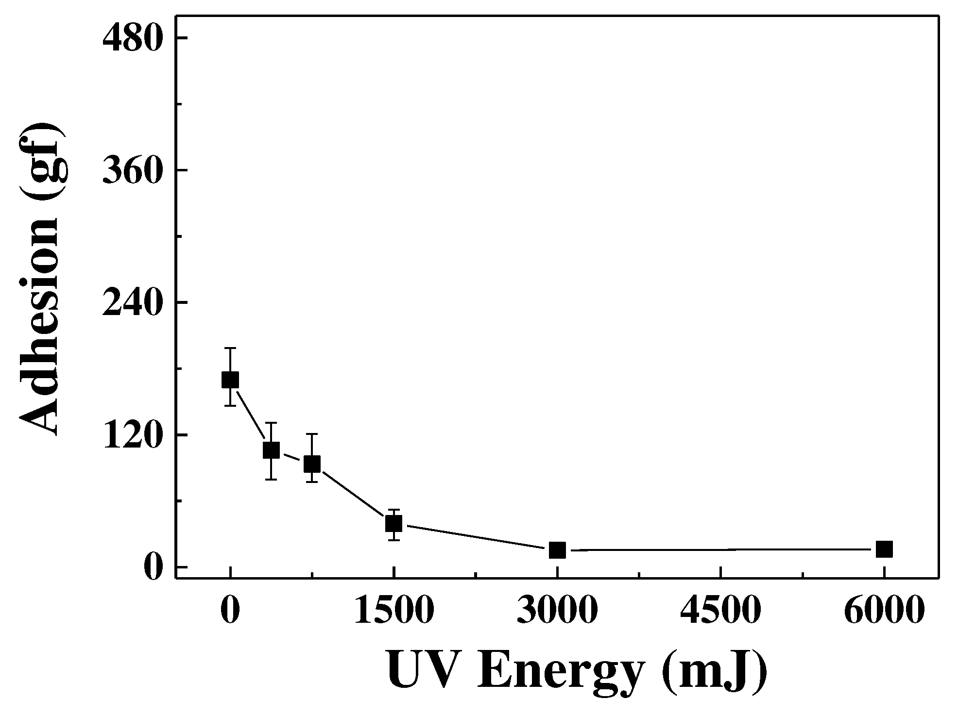
3.1. The Effect of UV Irradiation Energy on the Adhesion Strength
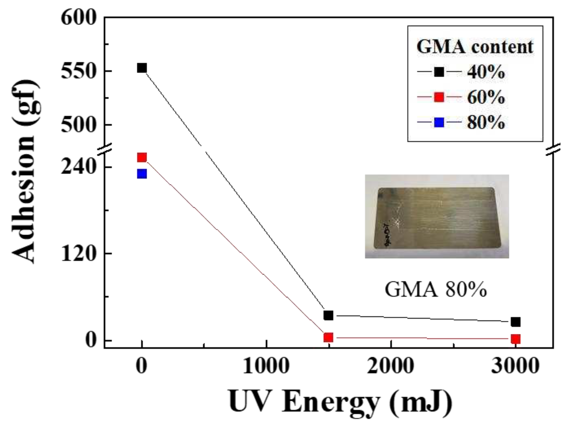
3.2. The Effects of GMA Content on the Adhesive Characteristics
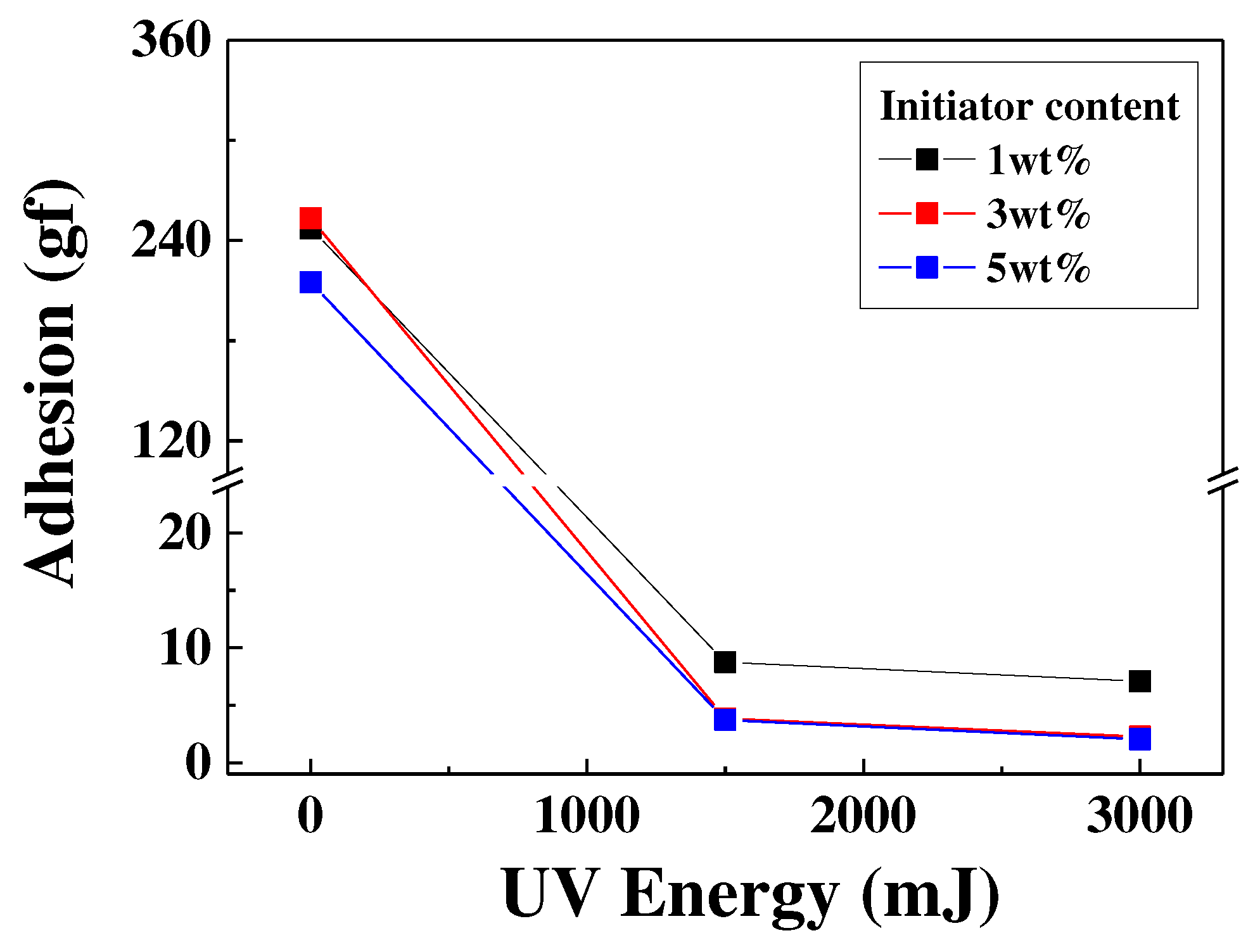
3.3. The Effects of Photoinitiator Content on the Adhesive Characteristics
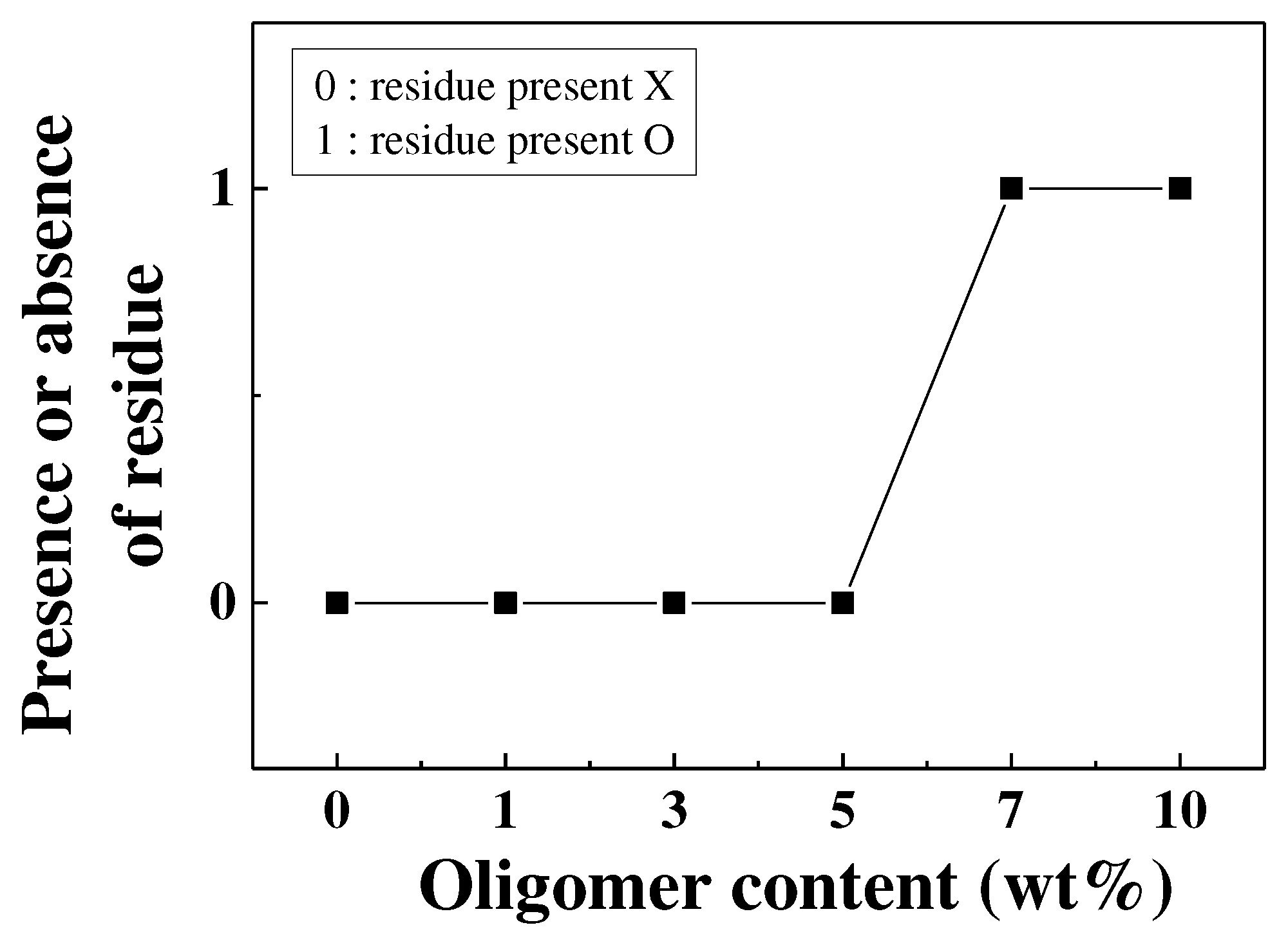
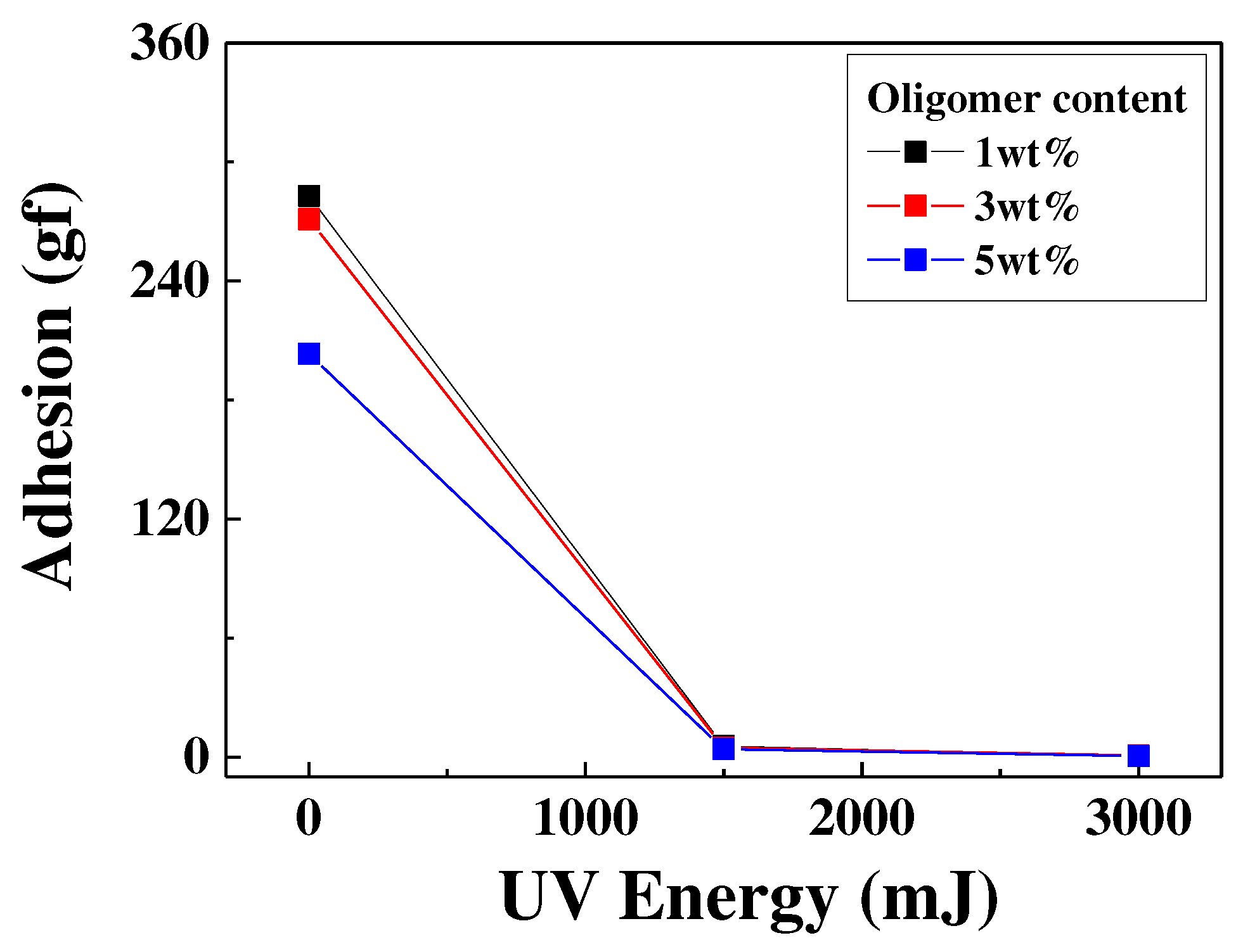
3.4. The Effect of Oligomer Content on the Adhesive Characteristics
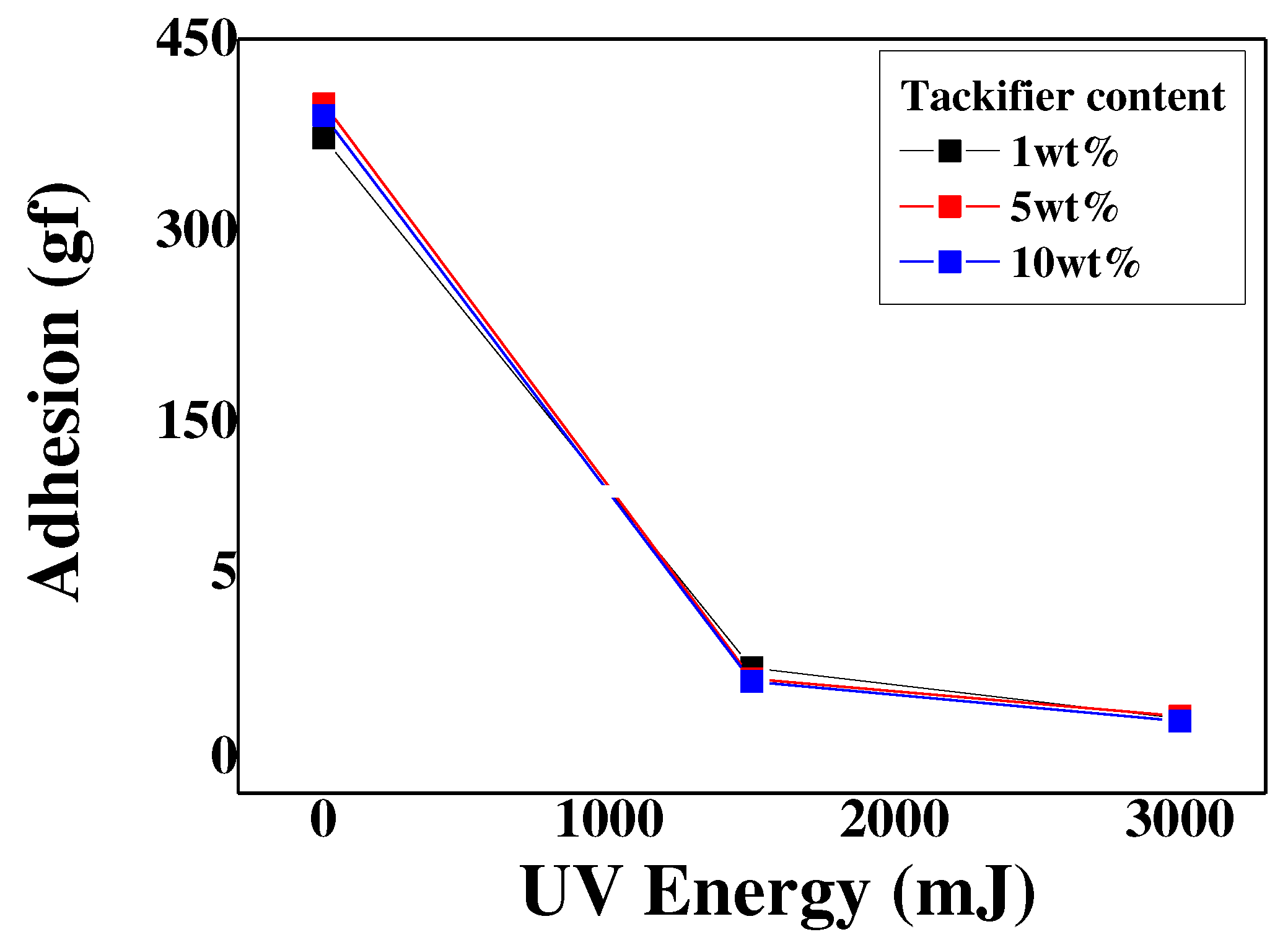
3.4. The Effect of Takifier Content on the Adhesive Characteristics
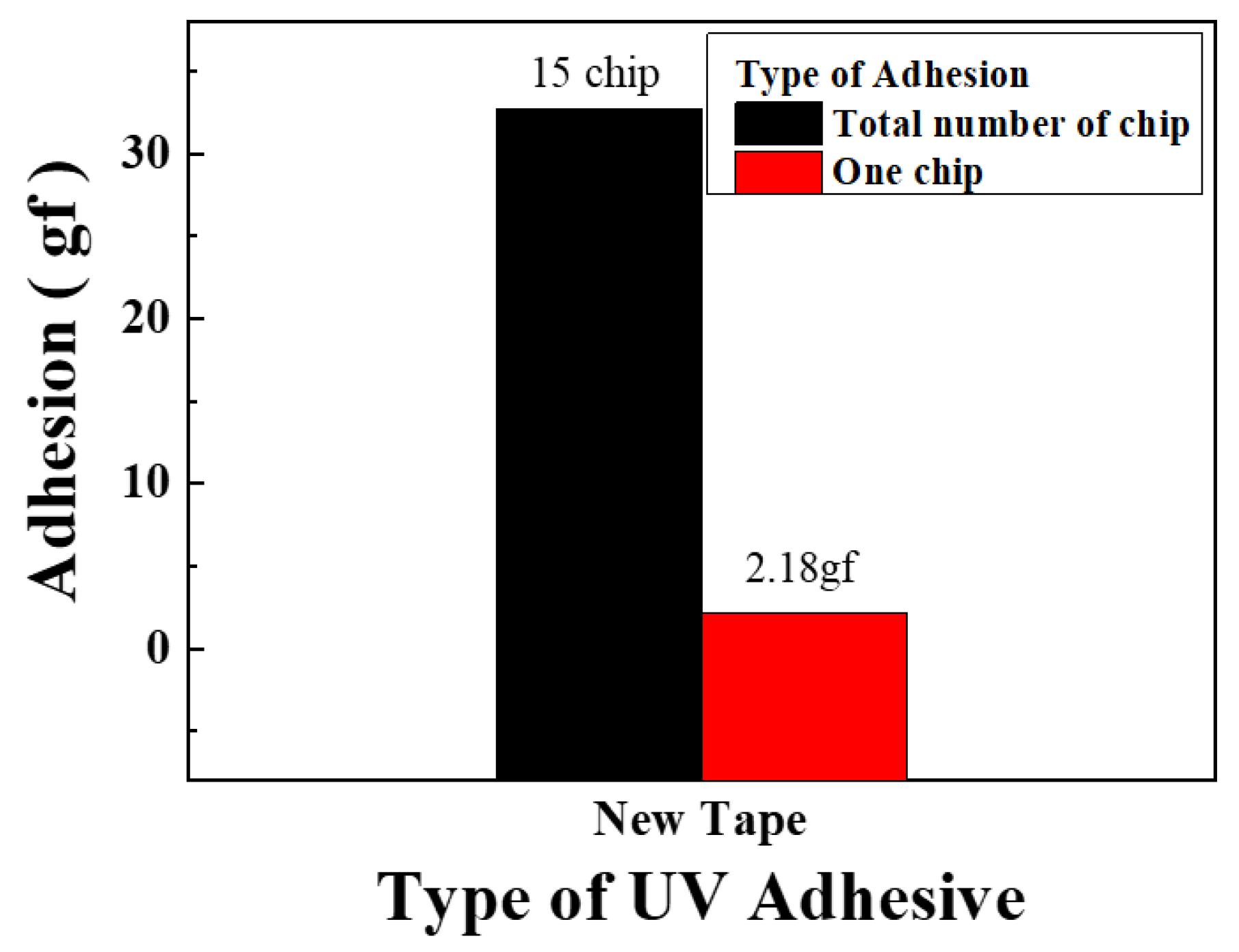
3.5. Removal of the Microchip
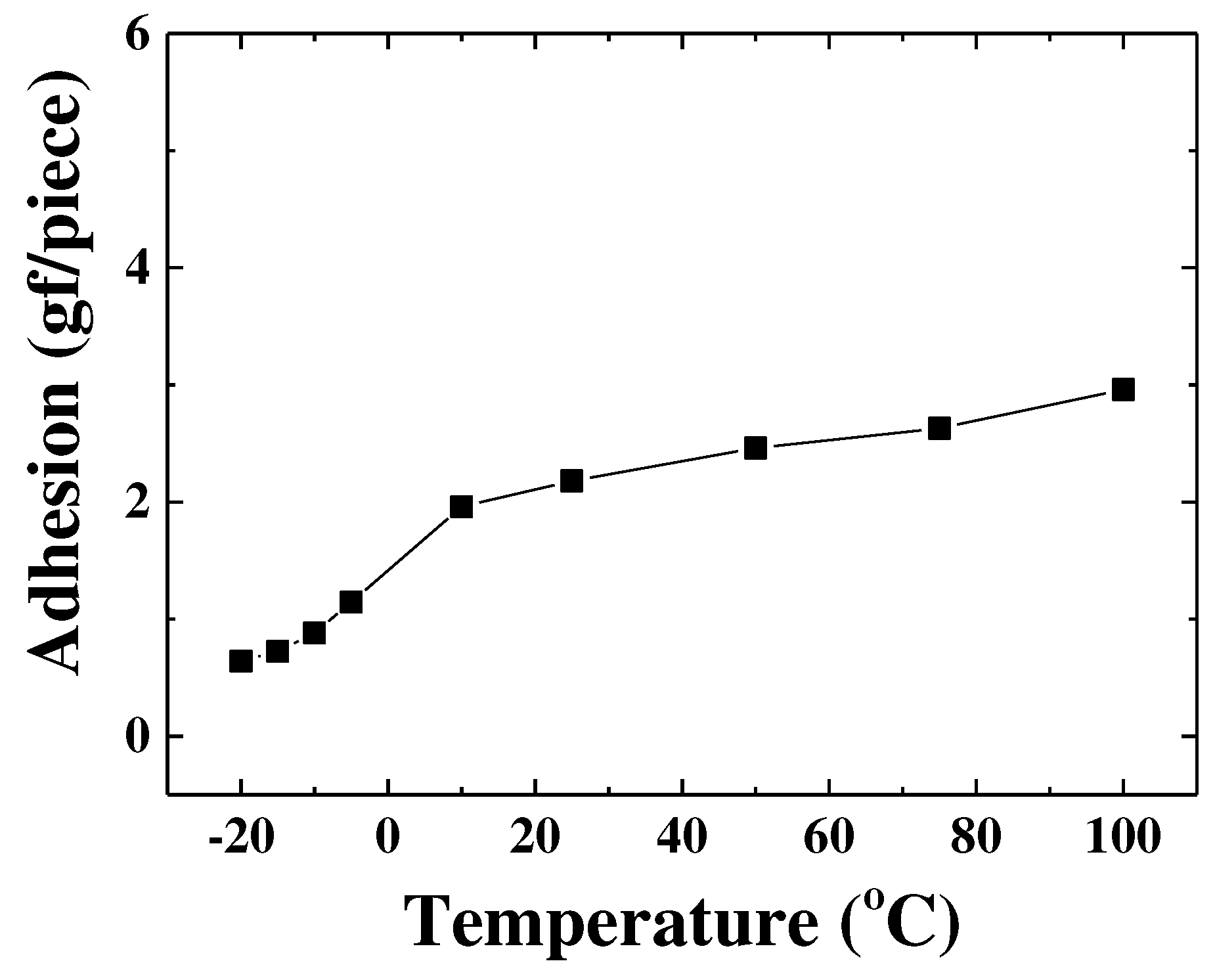
3.5. The Effect of Temperature on the Adhesion Characteristics
4. Conclusions
References
- Jelinek, Len. "Global semiconductor market trends." IHS Markit, May 2018.
- Burkacky, Ondrej, Julia Dragon, and Nikolaus Lehmann. "The semiconductor decade: A trillion-dollar industry." McKinsey & Company 1 (2022).
- Sweeney, Terence, Sonya Coleman, and Dermot Kerr. "Deep Learning for Semiconductor Defect Classification." 2022 IEEE 20th International Conference on Industrial Informatics (INDIN). IEEE, 2022.
- Lin, J. T., and Chen, C.-M. "Simulation optimization approach for hybrid flow shop scheduling problem in semiconductor back-end manufacturing." Simul. Model. Pract. Th. 51 (2015): 100-114. [CrossRef]
- Lee, S. H.,Lee, S. G., and Hwang, T. S. "Synthetic and adhesive properties of UV-curable acrylic adhesives for semiconductor manufacturing processes." Ind. Chem. 24.2 (2013): 148-154.
- Park., M. S. "Basic Technology of UV Curing Adhesives and Recent Technology Trends." Inform. Display 19.5 (2018): 21-28.
- Kim, S. Y. "The Hardening Behavior and Adhesive Properties of Acrylic Adhesives Using Inorganic Chillates." Adhesion and Interface 9.3 (2008): 27-33.
- Takyu, Shinya, Tetsuya Kurosawa, and Akira Tomono. "Novel DAF (Die Attach Film) separation technologies for ultra-thin chip." 2012 2nd IEEE CPMT Symposium Japan. IEEE, 2012.
- Ogasawara, T., Saiki, N., and Takyu, S. "Quantitative investigation of pick-up performance for UV-curable dicing tape." 2018 IEEE CPMT Symposium Japan (ICSJ). IEEE, 2018.
- Kumagai, Masayoshi, et al. "Advanced dicing technology for semiconductor wafer—stealth dicing." IEEE Transactions on Semiconductor Manufacturing 20.3 (2007): 259-265. [CrossRef]
- Kim, Keunhoi, et al. "Development of Semiconductor Packaging Technology using Dicing Die Attach Film." Journal of the Sensors Society 31.6 (2022): 361-365.9. Lee, S.W. "Application of Debonding Technology and Adhesive Materials for Semiconductor Packaging Process." Polym. Sci. Technol, 26.1 (2015): 40-46.
- Horigome, K., Ebe, K., Kuroda, and S.-i. "UV curable pressure-sensitive adhesives for fabricating semiconductors. I. Development of easily peelable dicing tapes." J. Appl. Polym. Sci. 90.2 (2003): 436-441.
- Hunskaar, Steinar, Odd-Geir Berge, and Kjell Hole. "A modified hot-plate test sensitivie to mild analgesics." Behavioural brain research 21.2 (1986): 101-108. [CrossRef]
- Ardévol, A. "Cooling rates of tissue samples during freezing with liquid nitrogen."J. Biochem. Bioph. Meth. 27.1 (1993): 77-86. [CrossRef]
- Moon, J.-I., et al. "Physical Properties of UV-Curable Powder Coatings with Different Photoinitiator Contents." J. Adhes. Interface 9.2 (2008): 32-37.
- Park, Y. J., Joo, H. S., Do, H. S., & Kim, H. J. (2006). Viscoelastic and adhesion properties of EVA/tackifier/wax ternary blend systems as hot-melt adhesives. Journal of adhesion science and technology, 20(14), 1561-1571. [CrossRef]



Disclaimer/Publisher’s Note: The statements, opinions and data contained in all publications are solely those of the individual author(s) and contributor(s) and not of MDPI and/or the editor(s). MDPI and/or the editor(s) disclaim responsibility for any injury to people or property resulting from any ideas, methods, instructions or products referred to in the content. |
© 2023 by the authors. Licensee MDPI, Basel, Switzerland. This article is an open access article distributed under the terms and conditions of the Creative Commons Attribution (CC BY) license (http://creativecommons.org/licenses/by/4.0/).


