1. Introduction
Over the past few decades, extreme events such as natural disasters, cyber-attacks, power system equipment failures, and power thefts have increased, eventually impacting the power system infrastructure, including distribution systems [
1]. Consequently, a power system blackout may occur, affecting people's social and economic life [
2]. As traditional power system networks are large ring systems, an extreme event may affect many loads and components [
3]. However, much research has been carried out in the area of power system migration, where the main aim was to convert from bulk power networks to small-scale networks [
4,
5]. The small-scale networks have been established through the development of renewable energies (RESs) and their integration into bulk power networks [
6], for example, microgrids (MGs) and smart grids (SGs). These are generally connected to the bulk power system, making them a grid-connected mode [
7,
8]. Further, it can change to the islanded mode while in events to avoid corresponding impacts on the distribution system and supply the local loads [
9]. Furthermore, the deployment of MGs and SGs can enhance system reliability and resiliency of the power distribution system in responding to extreme operating conditions.
As noted, it has been seen that the integration of RESs has increased during the past few decades, which plays a crucial role in the distribution systems for grid modernization [
10]. However, due to the intermittency of the RESs, it has certain challenges, which make the system complex and unstable. The most noticeable challenge is uncertainty, which means it depends on environmental factors such as solar insolation and wind speed for solar and wind systems, respectively [
11]. To deal with these challenges, the advanced power electronics in distribution systems play a crucial role in regard to the control of power (both active and reactive power) flow to enable DC-operated technology[
12], protection [
13], mitigating the power quality issues, and reducing harmonics. To address these benefits, power electronics are reconfigured in a different way to make it possible for the determination of power quality problems [
14]. It is critical for the distribution networks that the reliability factor is always a prime concern—with this objective, using a modern power electronics device, a solid-state device is pronounced, named as the SST. SST is treated as an evolving technology for providing power supply to the consumer through MGs or SGs [
15]. Besides, the SST is a high-frequency transformer with a power electronic converter and is an alternative to the traditional bulky and non-smart transformer.
In the past decades, researchers have shown interest in modeling and the development of SST for MG and SG applications. In [
16,
17], the design and response of SSTs are addressed through their converter stages and controllers. In [
18], average models and their controllers are proposed and explored through descriptive simulation studies. Further, in [
19], the stability aspect of SST and validation, which has been done through the distribution system, is presented. In this regard, many motivating test models of transient instabilities have been developed, and their importance to the link topologies of SSTs in various operating regions is demonstrated [
20]. The most prominent manufacturers of SST, namely, ABB, ETH Zurich, EPRI, Siemens, and FREEDM Systems Center, have conducted cutting-edge research to upgrade the conventional transformer to an intelligent one. They have designed and tested various topologies to improve the performance and facilities of SST to the connected devices [
21,
22,
23,
24,
25,
26]. In [
26], the FREEDM Systems Center is presented with a start-up SST structure named Generation-1-SST, which can be used in medium-voltage-based MG. Further development has been done with a multi-cell-based DC-DC converter for SST, which is proposed in [
27]. However, the research on SST stability is lacking in the literature and must be considered a vital factor. Thus, the stability aspect of each stage (input, isolation, and output) of the SST needs to be emphasized, which this paper addresses. The main contribution of this work is detailed as follows.
This study develops a state-space and a transfer-function-based model with a proper SST controller to reduce system complexity and cost. The state-space parameters (A, B, C, and D) of the converter's input, insolation, and output stages are estimated. Each converter stage has its own controller and filter circuit. The PI controller is implemented in this design due to its simplicity, robustness, and excellent control action. The transfer function model of each converter is derived from the state-space model. By using the transfer function equation, the stability of the proposed design is tested in terms of frequency response, time response, controllability, and observability. Furthermore, the Simulink design of the proposed system is established in Matlab software, and the controller is designed through MATLAB SISOTOOL. The state-space model is designed for the stability study with and without a controller. In the proposed methodology, the user can simply design the controller part from the unstable model through MATLAB SISOTOOL, thereby making the system robust and stable. Thus, researchers can easily measure the system's stability, sensitivity, controllability, and observability.
This article is organized as follows.
Section 1 provides an introduction to SST and a literature review.
Section 2 outlines the fundamentals and different types of SST topology. In
Section 3, the continuous-time average state-space model and its transfer function model are formulated. In this section, the converter stage is categorized into the input, isolation, and output stages. Then, each stage's state, model, and control parameters are derived. Finally, the result and discussion parts of the proposed model are provided in
Section 4, followed by the conclusions in
Section 5.
2. Fundamental topologies of SST
Various architectures are available for each of the three stages of SST. The topology is determined depending on the application of SST. The different types of topologies are Type-A (A-1 and A-2), Type-B, Type-C, Type-D, and Type-E [
28]. This study adopts the Type-D-based SST topology [32] because it has numerous advantages, such as DC connectivity, fault isolation, proper voltage regulation, easy integration with RESs and storage, and volt-ampere reactive (VAR) compensation. In the design, the architecture for each stage should be chosen appropriately, and the problems should be addressed by integrating them into a single system to deliver regulated voltage at each stage.
The fundamental three-stage architecture of SST is presented in
Figure 1. The input stage, which is also called the AC–DC stage, contains a single-phase AC–DC IGBT-based converter that operates at a high switching frequency. The isolation stage, which is also called the DC-DC stage, comprises two H-bridges with a high-frequency transformer. A DAB converter is also applied in this stage [
29]. The output of the input stage is fed to the DAB converter, and the output of the converter is fed to the inverter or is considered the output stage. In the output stage, a filter circuit is added to mitigate the voltage and power quality issues. The output stage is usually supplied to low-voltage user applications.
3. Continuous-time average state-space model
In this section, the design of the state-space model and the continuous-time transfer function model is formulated. The controller of each stage is derived to enhance system stability and performance. Furthermore, the different parameters are calculated and presented in tables to determine the stability, frequency level range, and DC gain of each stage.
3.1. Input stage (AC-DC)
Formulation: The input stage of the SST is the conversion of AC to DC signal, shown as architecture and equivalent diagram in
Figure 2. (a) and
Figure 2. (b), respectively. Eq. (1) and Eq. (2) represent the input voltage; however, in Eq. (2), the duty cycle is taken as an average over a switching time. Referred to
Figure 2. (b), Eq. (3) is formed by applying the KVL equation. Further, considering changes as a minute value in the DC signal, Eq. (3) can be modified as Eq. (4). Eq. (5) is solved by having Eq. (3) and Eq. (4). Thereafter, by applying Laplace transform to Eq. (5), Eq. (6) and its updated version in Eq. (7) are obtained, which represent the open-loop transfer function of the input stage with the inductor current.
Further, the transfer function of the input stage through DC-link capacitance current is presented in Eq. (8). Similarly, Eq. (9)-(11) is solved to reach Eq. (12), which represents the ratio of the change in output DC link voltage to any change in input current.
State Space Model: Furthermore, the state-space model presented in Eq. (13) and (14) denotes the state and output equation of the system where A, B, C, and D are the state, control, output, and transmission matrices, respectively. The overall transfer function of the input stage has been derived, and the state space parameters are measured in the results section [
30]. Here
is the state variable, which are: inductor current (
) and capacitor voltage (
and
is the input as
.
Considering the input stage transfer function as derived in (7) and (12), two controllers have been designed using MATLAB SISOTOOL. Thus, corresponding to
and
, the PI controllers are
and
, respectively.
3.2. Isolation stage (DC-DC)
In this stage, the DAB converter is considered for DC-DC conversion. A high-frequency transformer is placed between DAB, as depicted in
Figure 4. (a), and the equivalent diagram is depicted in
Figure 4. (b). The DAB converter deals with three main parameters, namely, phase shift between two bridges (Ø), duty cycle ratios (D), and switching frequency (fs). The other parameters are as follows:
represents the equivalent of winding resistance and switching on resistance;
is the leakage inductance of the proposed transformer referred to as the secondary side;
,
,
,
,
,
, and
are the converter switches; and
, and
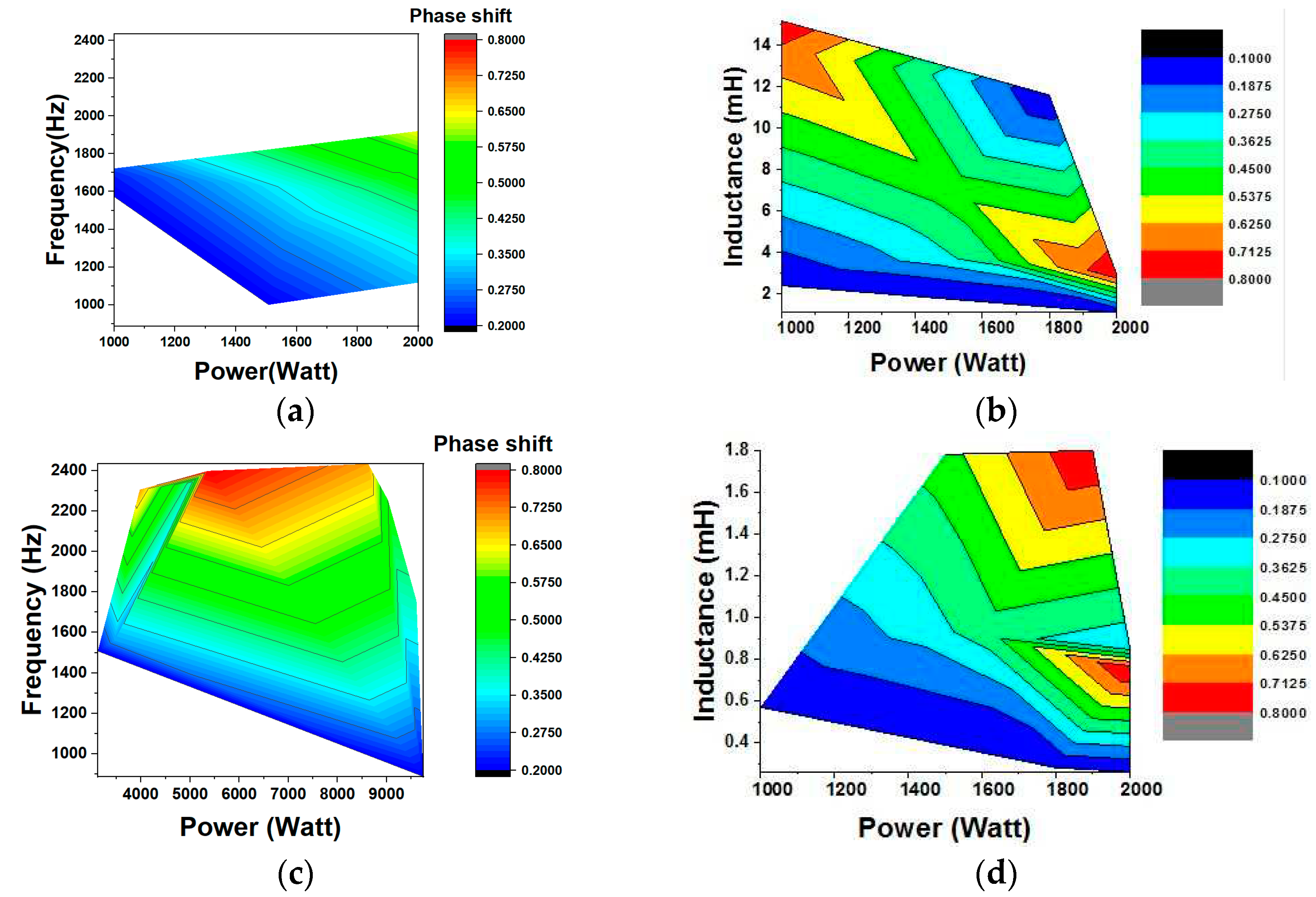
are the primary and secondary winding voltages, respectively. The leakage inductance is calculated using Eq. (20). Refer to Eq. (15), the variation in transformer output with different frequencies and leakage inductance is shown in
Figure 5.
Moreover, the duty cycle ratio of the proposed scheme is fixed to 0.5. Subsequently, the phase shift modulation technique is used here to control the operation of DAB. The transferred power from one stage of DAB to the other stage can be expressed in Eq. (16). Further, the state-space model of the DAB can be formulated as Eq. (17) by assuming the two-state variables of the proposed systems, namely, the current through the inductor (
) and the voltage across the capacitor (
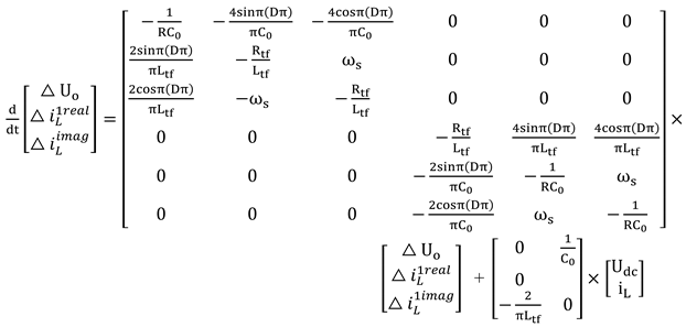
). Eqs. (17) and (18) are time-variant and nonlinear. To ensure that the system is time-invariant and linear, the traditional state-space averaging procedure is applied to characterize a state variable x(t) by utilizing its Fourier series expansion as given in Eq. (19). When the Fourier analysis is applied in Eqs. (17) and (18), Eq. (20)-(25) are obtained. In this Fourier analysis, only the 0
th and 1
th order terms are considered, while other higher-order terms of state variables are neglected.
here,
where ω =2πf and X
k(t) is the k
th coefficient in the Fourier series analysis.
The transient behavior of the DAB converter in terms of voltage variations is considerably slower in the input than in the output. Therefore, the 0
th term of input voltage is
=
and
=
. The transient behavior of the first term of input voltage and load current is neglected, which are
and
. In this design, the converters are operating in 50% of the duty cycle. Thus, the first-order terms of
(t) and
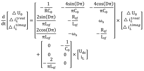
(t) are similar to zero order and are presented in Eqs. (26)-(29). Moreover, in Eqs. (17) and (18), the independent state variables are the inductor current and capacitor voltage, which form the state-space model of the DAB converter with the state vector x(t) and the control vector u(t). Further, Eqs. (30) and (31) represent the state-space model with the input and output signals of the DAB converter. Therefore, the model parameters are input voltage source (
), inductor current (
), and duty cycle (D). When
and
are introduced into Eqs. (20), and (25), the state-space model becomes Eq. (31). Furthermore, the zero initial states are assumed in Eq. (32), which are,
,
,
are similar to zero order, and Eq. (32) becomes Eq. (33).
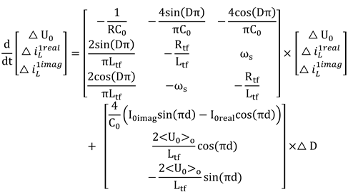
A small signal control for the output transfer function is needed to measure the system stability of the DAB converter with the controller structure. Thus, a small deviation in D causes a distinction in the values of
from its steady-state value. Hence, the corresponding small signal model is defined in Eqs. (34)-(37). In addition, the nonlinearity of the system is introduced when the control and state variables are multiplied. The approximation solution of nonlinear terms is presented in Eq. (38). To this end, given the value of parameters defined in Eqs. (34)-(37) are placed into Eq. (33), then the state-space model can be expressed as in Eq. (39) while the corresponding values are given in A, B, C, and D matrix form. Further, the transfer function of the DAB converter can be expressed using a conversion formula, which is given in Eq. (40), and the values are assigned and given in Eq. (41), where
is the open-loop transfer function of the DAB.
3.3. Output (DC-AC) stage
The DC-AC stage architecture and the equivalent diagram are presented in
Figure 6 (a) and
Figure 6 (b), respectively. Based on Figure. 6 (b), the KVL is applied and can be expressed as Eq. (42), followed by Eqs. (43) and (44). Further, the voltage across the capacitor and current through the load and capacitor are presented in Eqs. (45), (46), and (47), respectively. Eq. (48) denotes the inverter output. Thereafter, a small signal change was applied to Eq. (44), Eqs. (49) and (50) are obtained. Then, applying the Laplace transform to Eq. (50) yields Eq. (51), and the ratio is presented in Eq. (52). In order to smoothen the output signal, a filter circuit is added, which is formulated in Eq. (53), and the final equation is given in Eq. (54). Further, using Eqs. (52) and (54), the obtained equations are Eqs. (55) and (56). Eq. (57) represents the closed-loop transfer function of the output (DC-AC) stage converter. However, this closed-loop transfer function is designed without a controller. Thus, to design a controller with this transfer function, MATLAB SISOTOOL is used, and the final transfer function becomes Eq. (58). Subsequently, the state space parameters are found using Eq. (58), and then controllability and observability are tested in
Section 4.
The state-space matrix of the above-mentioned equation is given as
4. Results and discussion
The overall model of the system is developed by concatenating the models of individual parts.
4.1. Time domain and frequency domain analysis
The proposed SST model is designed and analyzed in terms of time response, frequency response, and state-space characteristics. The time response analysis is conducted by the root locus technique, which determines the absolute stability and shows the location of poles or zeros in the s-plane. This technique also determines the physical performance of the model when the gain of the input to the plant is changed from 0 to. The technique is advantageous in controller design because it is organized and saves energy and time. This study is limited to the linearized model, and both eigen analysis and frequency domain testing are applied to the linear model. In addition, time-domain analysis is studied.
Input stage numerical study: To ensure the stable operation of the system, a controller is added through MATLAB SISIOTOOL, given in Eq. (59) and (60) for
and
, respectively. The overall closed-loop transfer function of the input stage converter is given by Eq. (61).
Input stage controllability and observability test: To test the system controllability and observability, the controllable matrix (Mc) and observable matrix (Mo) can be measured, which are expressed in Eq. (62) and Eq. (63), respectively, while their corresponding values are given below. Given the matrices
and
, the ranks of both are 4, which signifies the system is controllable and observable because the ranks of matrics (Mc and Mo) are the same as 4.
Isolation stage controllability and observability test: To test the system controllability and observability, the controllable and observable matrices as
and
respectively, and the values are given below.
From the Mc and Mo, the ranks of both are 3, which signifies the system is controllable and observable. To ensure the stability of the system and its closed-loop function, a feedback controller and a filter circuit must be added, which is expressed in Eq. (64). The corresponding state-space parameter
and followed by the test matrix (controllable and observable matrix) of the isolation stage are shown below, which is also controllable and observable because the rank of the matrix is the same as that of the test matrix. Further, the closed-loop transfer function of the proposed DAB converter is expressed in Eqs. (65) and after the assigned value, it is presented in Eq. (66).
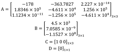
The corresponding A, B, C, and D matrix are:
Output stage controllability and observability test: This sub-section is similar to Sections 3.1.1 and 3.2.1. As in Eqs. (62) and (63),
and
are controllable and observable matrices, and the values are given below. The ranks of these matrices are 3, which signifies the system is controllable and observable, which subsequently means that the output stage is controllable and observable.
The stability criterion is shown in
Table 1. Further, the performance index is measured through frequency domain analysis and presented in
Table 2 for the input, isolation, and output stages.
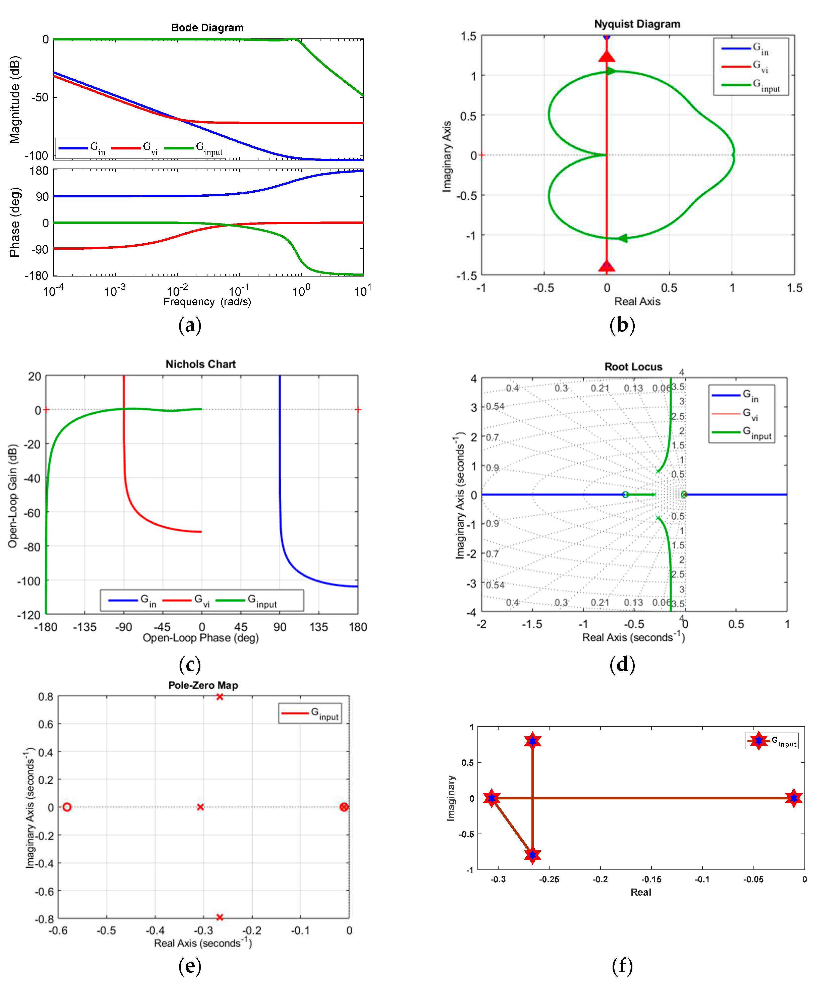
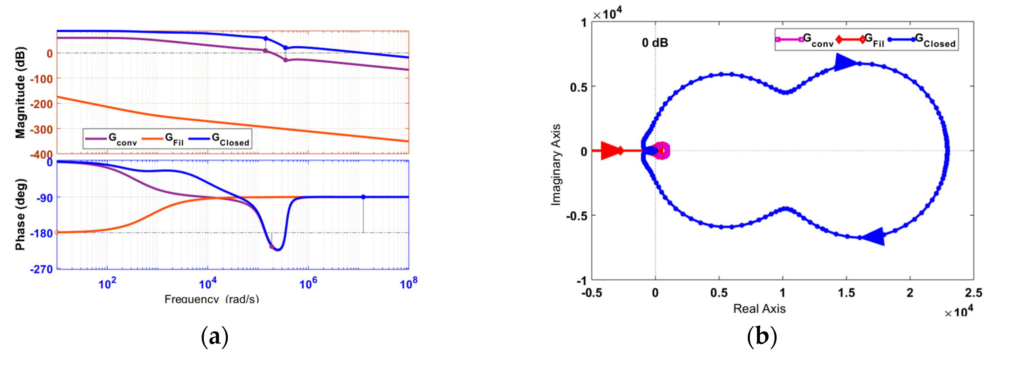
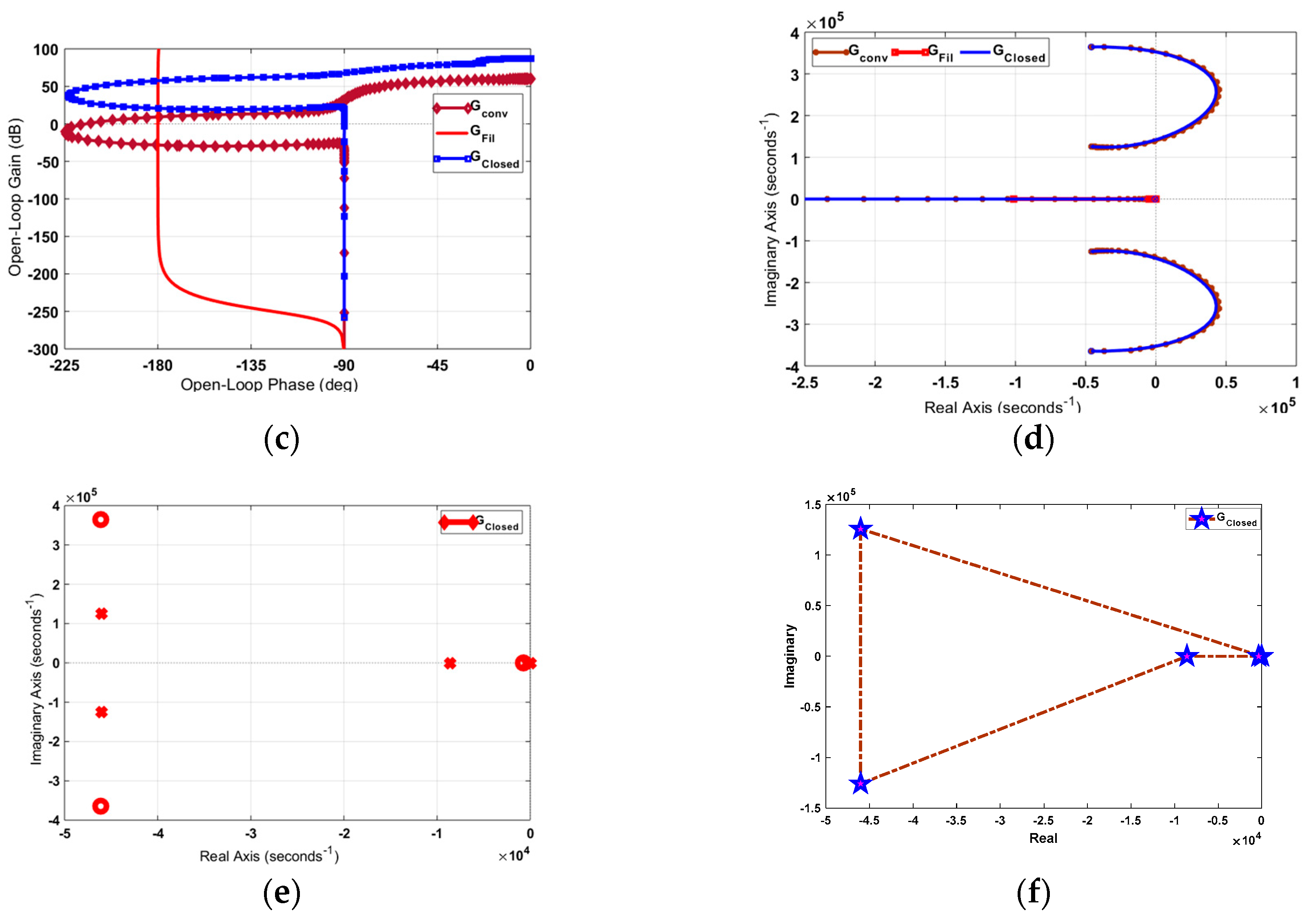
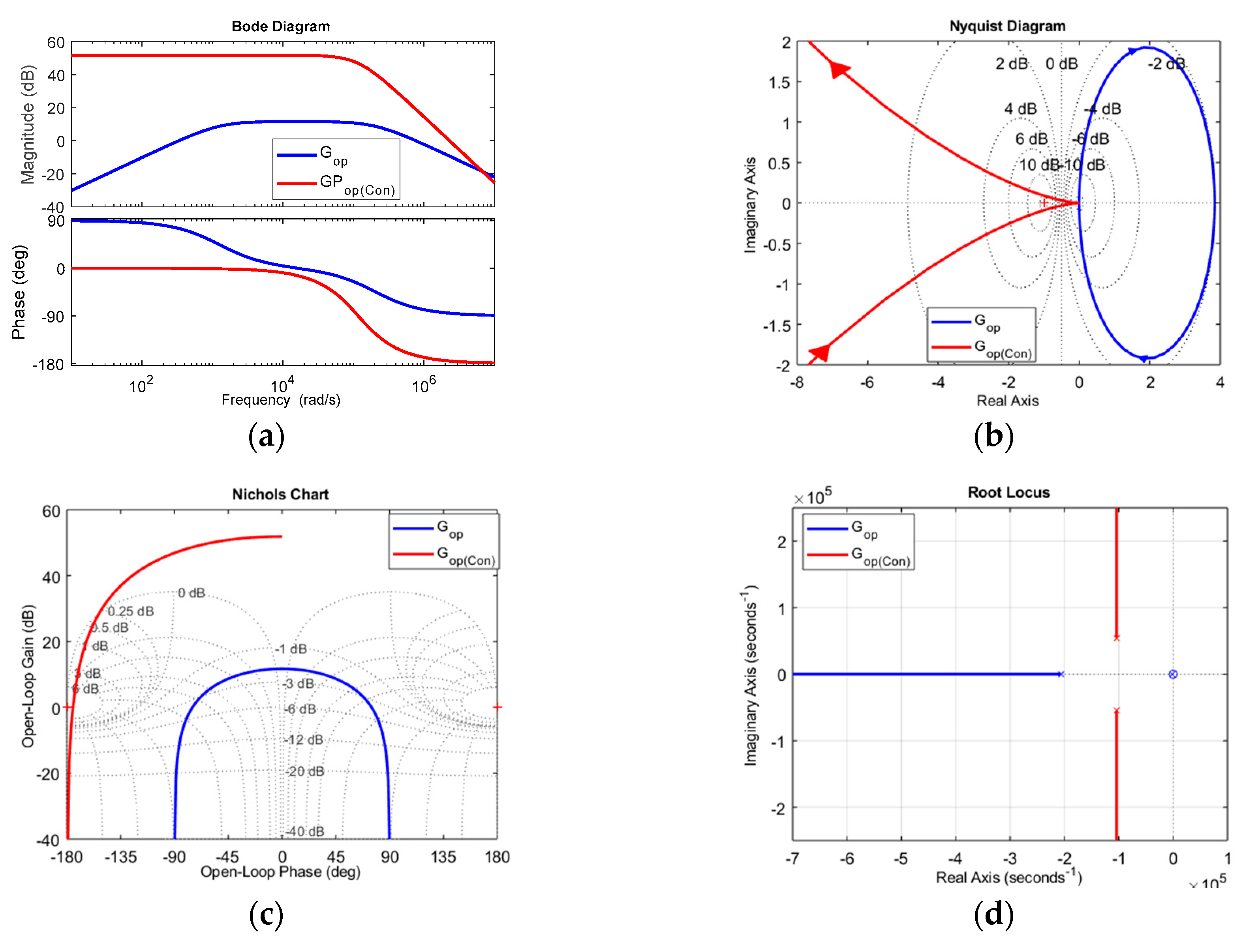
The Bode diagram reflects the variation in magnitude and phase with respect to frequency level at a log scale. Various parameters, such as GM, PM, ωcg, and ωcp, can be measured from the Bode plot. Thus, system stability margins can be determined. The Nyquist plot reflects the relationship between the imaginary part of the closed-loop transfer function and the radial frequency (ω) in the real axis with the variation in 'ω' from zero to infinite in the polar coordinate. This plot determines the absolute and relative stability even if the system has delays in practical assumption. The plot also provides information such as GM, PM, BW,
, and
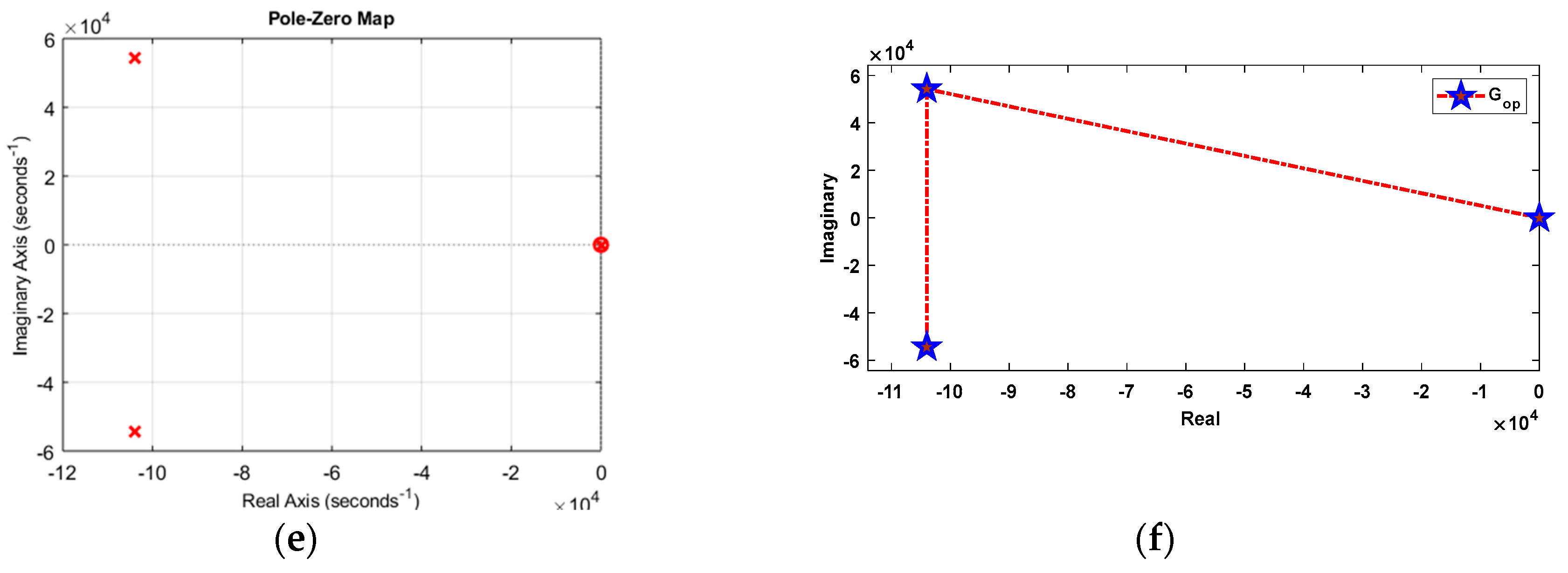
. The Nichols plot is the extension of the polar plot. In this plot, magnitude and phase-angle loci at log scale versus phase diagram are in the imaginary and real axes. The location of poles and zeros of the system is presented in the pole-zero plot, and the eigenvalue of each converter in the form of a graph is depicted in
Figure 7,
Figure 8 and
Figure 9 for the input, isolation, and output stages, respectively.
4.2. Simulation results analysis
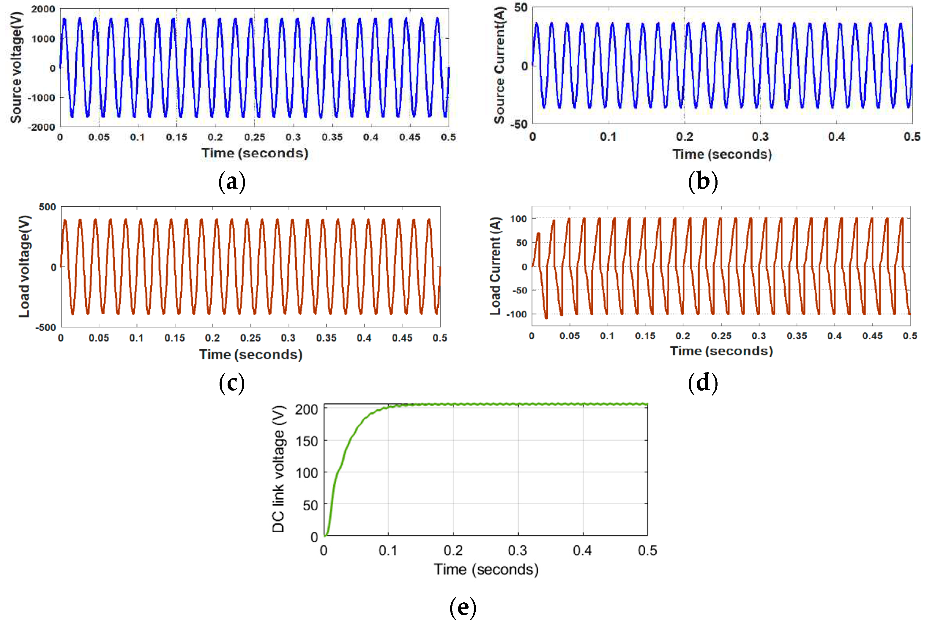
In this section, the simulation results of the three-stage SST are shown. The source voltage, source current, load voltage, load current, and DC-link voltage after completion of SST simulation are shown in Figure. 10. The behavior of the input remains the same, even if the load side transient is disturbed. Thus, SST provides excellent isolation through the DAB converter and maintains the same phase angle at the input stage.
4.3. Hardware-in-the-loop (HIL) validation
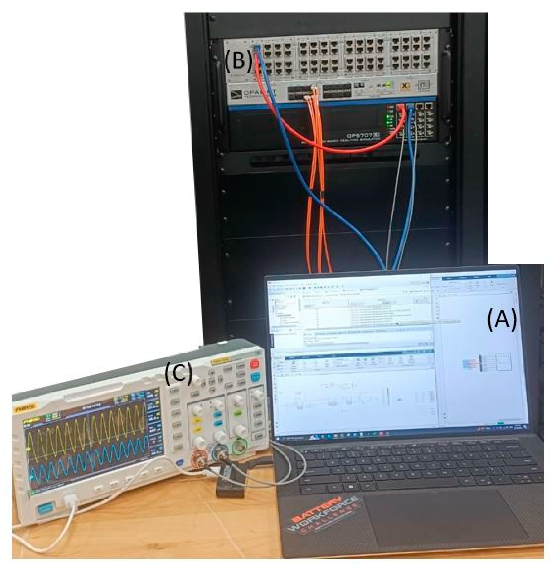
Furthermore, the Simulink model of SST has been built and executed in real-time simulation using the OPAL-RT simulator. The specification of the real-time digital simulator is OP5707XG, Intel® Xeon® processing cores with the power of a Xilinx® Virtex®-7 FPGA. The RT lab 2020 is installed on our laptop with a specification of 13th Gen Intel(R) Core(TM) i7-1355U 1.70 GHz, 64-bit operating system.
This key action marks a major advancement in the pursuit of accuracy and real-world application. The incorporation of OPAL-RT as hardware-in-the-loop (HIL) simulation is crucial and facilitates the transition between virtual and physical systems. The proposed SST model has been developed with hardware synchronization using OPAL-RT, creating an environment closely resembling real-world situations.
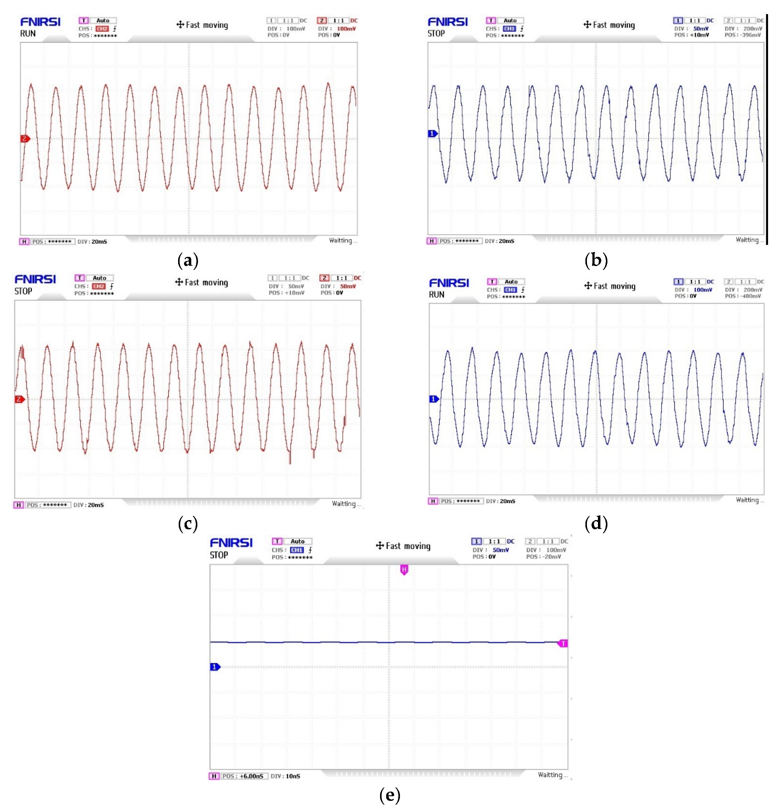
Figure 11 represents the HIL setup, where the SST model has been developed using RT Lab (a), synchronized through the OPAL-RT simulator (b), and the output can be observed on an oscilloscope (c). Furthermore, the performance of the HIL model of SST is presented in
Figure 12. The input voltage and current are displayed in
Figure 12 (a) and (b), while the output voltage and current are shown in
Figure 12. (c) and (d), respectively. The DAB output can be observed in Figure. 12 (e). Based on the HIL results, it can be concluded that it exhibits the exact performance of the Simulink model, as presented in Figure. 10. The implementation of the proposed SST Simulink model with OPAL-RT for HIL simulation has been successfully validated, representing a significant accomplishment in our research and development work. This makes the proposed SST model more credible and ensures that our considerations are not limited to the virtual world but have relevance to the complexities of the actual world.
5. Conclusions
In this study, a state-space model is established to measure the stability of each converter stage for determining the system performance with and without a controller. The analysis is conducted in three phases. In an initial attempt, the state-space model of the converters is developed and expressed in terms of state-space parameters (A, B, C, and D) and is tested over controllability and observability matrices for measuring the system state. The transfer function model is formulated from the state-space parameters and applied to the frequency and time domain analysis to draw the Bode plot, Nyquist, Nichols, and root locus plot. On the basis of these plots, the stability, DC gain, peak resonant, and eigenvalue of the system are measured. Further, the Simulink design is simulated, and the results are provided, validating the systems' characteristics and seen as smooth performances. Finally, the Simulink model has been validated using a real-time digital simulator, such as OPAL-RT, which is considered an HIL simulation, and its performance exactly matches the simulation results.
This study has particularly drawn attention to the transient performance and the stability of the system, which can be analyzed using the proposed approach, such as the state-space and transfer function-based model. The proposed SST model can be implemented in different applications. In particular, in distribution system applications, it has minimal impact on voltage disturbance and can manage the fluctuation caused by intermittent sources, like solar and wind. With these features, the SST can play an essential smart component to make it a resilient distribution system.
Author Contributions
Conceptualization, D.K.M. and M.H.A.; methodology, D.K.M.; software, D.K.M.; validation, D.K.M., S.P, and S.K.S; formal analysis, D.K.M., M.E and L.L.; investigation, D.K.M., M.E. and S.K.S.; resources, D.K.M. and J.Z; data curation, D.K.M.; writing—original draft preparation, D.K.M. and M.E; writing—review and editing, D.K.M. M.H.A, S.P, and J.Z; visualization, D.K.M.; supervision, L.L., and J.Z; project administration, D.K.M., and M.E; funding acquisition, D.K.M, JZ, and L.L. All authors have read and agreed to the published version of the manuscript.
Conflicts of Interest
The authors declare no conflict of interest.
Bibilogpahy
AC: Alternating current
BW: Bandwidth
DAB: Dual Active Bridge
DC: Direct current
D: Duty cycle
GM: Gain margin
HF: High frequency
MF: Medium frequency
PWM: Pulse width modulation
PM: Phase margin
SST: Solid State Transformer
MGs: Microgrids
N: Turns ratio
Z: Load
U: Voltage
F: Frequency
L: Leakage inductance
ɸ: Phase shift
db: decibel
SGs: Smart-grids
: Identity matrix
: input voltage
: dc link voltage
: peak ac input voltage
: inverter output voltage
: voltage across the capacitor
: duty cycle
: averaged duty cycle
: output stage duty cycle
A small change in the duty cycle
: modulation index
R= resistance at the isolation stage
: Inductor at the input, isolation, and output stage
: capacitor at the input, isolation, and output stage
Ltf & Rtf: Transformer equivalent inductance and resistance
: input current
: current through capacitor
: load current
: current through inductor at the output stage
: change in input current
and : current and voltage control loop transfer function of the input stage
: open loop transfer function of the isolation stage
: transfer function of the output stage without and with controller
: feedback controller for filter circuit for the output stage
= closed-loop transfer function of the output stage
and : PI controller for and fs: switching frequency
voltage across the capacitor
: current through the inductor
controllable and observable matrix
GM and PM: Gain and phase margin
BW: bandwidth
ωcg and ωcg: gain crossover and phase crossover frequency
: peak frequency and gain peak
DC gain
Appendix A
System parameter and its value
| Input stage |
Isolation stage |
Output stage |
|
=400V
Turns ratio : =1:1
Switching frequency=20kHz
|
=200V
|
References
- Wang, C.; Ju, P.; Wu, F.; Pan, X.; Wang, Z. A systematic review on power system resilience from the perspective of generation, network, and load. Renew. Sustain. Energy Rev. 2022, 167. [Google Scholar] [CrossRef]
- Mishra, D.K.; Ghadi, M.J.; Azizivahed, A.; Li, L.; Zhang, J. A review on resilience studies in active distribution systems. Renew. Sustain. Energy Rev. 2020, 135, 110201. [Google Scholar] [CrossRef]
- Guo, W.; Qureshi, N.M.F.; Jarwar, M.A.; Kim, J.; Shin, D.R. AI-oriented Smart Power System Transient Stability: The Rationality, Applications, Challenges and Future Opportunities. Sustain. Energy Technol. Assessments 2023, 56. [Google Scholar] [CrossRef]
- Kröger, W. Achieving Resilience of Large-Scale Engineered Infrastructure Systems, in Resilient Structures and Infrastructure. 2019, Springer. p. 289-313.
- Panteli, M.; Mancarella, P. The Grid: Stronger, Bigger, Smarter?: Presenting a Conceptual Framework of Power System Resilience. IEEE Power Energy Mag. 2015, 13, 58–66. [Google Scholar] [CrossRef]
- Du, P.; Baldick, R.; Tuohy, A. Integration of large-scale renewable energy into bulk power systems. Springer 2017, 10, 978–3. [Google Scholar]
- Wouters, C.; Fraga, E.S.; James, A.M. An energy integrated, multi-microgrid, MILP (mixed-integer linear programming) approach for residential distributed energy system planning–a South Australian case-study. Energy 2015, 85, 30–44. [Google Scholar] [CrossRef]
- Naebi, A.; SeyedShenava, S.; Contreras, J.; Ruiz, C.; Akbarimajd, A. EPEC approach for finding optimal day-ahead bidding strategy equilibria of multi-microgrids in active distribution networks. Int. J. Electr. Power Energy Syst. 2019, 117, 105702. [Google Scholar] [CrossRef]
- Wu, X.; Wang, Z.; Ding, T.; Wang, X.; Li, Z.; Li, F. Microgrid planning considering the resilience against contingencies. IET Gener. Transm. Distrib. 2019, 13, 3534–3548. [Google Scholar] [CrossRef]
- Schoene, J.; Humayun, M.; Russell, B.; Sun, G.; Bui, J.; Salazar, A.; Badayos, N.; Zhong, M.; Lak, M.; Clarke, C.R. Quantifying Performance of Distribution System State Estimators in Supporting Advanced Applications. IEEE Open Access J. Power Energy 2020, 7, 151–162. [Google Scholar] [CrossRef]
- Mishra, D.K.; Ray, P.K.; Li, L.; Zhang, J.; Hossain, M.; Mohanty, A. Resilient control based frequency regulation scheme of isolated microgrids considering cyber attack and parameter uncertainties. Appl. Energy 2021, 306, 118054. [Google Scholar] [CrossRef]
- Asadi, Y.; Eskandari, M.; Mansouri, M.; Savkin, A.V.; Pathan, E. Frequency and Voltage Control Techniques through Inverter-Interfaced Distributed Energy Resources in Microgrids: A Review. Energies 2022, 15, 8580. [Google Scholar] [CrossRef]
- Sun, Z.; Eskandari, M.; Zheng, C.; Li, M. Handling Computation Hardness and Time Complexity Issue of Battery Energy Storage Scheduling in Microgrids by Deep Reinforcement Learning. Energies 2022, 16, 90. [Google Scholar] [CrossRef]
- Gorjian, A.; Eskandari, M.; Moradi, M.H. Conservation Voltage Reduction in Modern Power Systems: Applications, Implementation, Quantification, and AI-Assisted Techniques. Energies 2023, 16, 2502. [Google Scholar] [CrossRef]
- Zhao, B.; Song, Q.; Li, J.; Liu, W.; Liu, G.; Zhao, Y. High-Frequency-Link DC Transformer Based on Switched Capacitor for Medium-Voltage DC Power Distribution Application. IEEE Trans. Power Electron. 2015, 31, 1–1. [Google Scholar] [CrossRef]
- She, X. , et al., Design and demonstration of a 3.6-kV–120-V/10-kVA solid-state transformer for smart grid application. IEEE Transactions on Power Electronics 2013, 29, 3982–3996. [Google Scholar] [CrossRef]
- Ortiz, G.; Uemura, H.; Bortis, D.; Kolar, J.W.; Apeldoorn, O. Modeling of Soft-Switching Losses of IGBTs in High-Power High-Efficiency Dual-Active-Bridge DC/DC Converters. IEEE Trans. Electron Devices 2013, 60, 587–597. [Google Scholar] [CrossRef]
- Zhao, T.; Zeng, J.; Bhattacharya, S.; Baran, M.E.; Huang, A.Q. An average model of solid state transformer for dynamic system simulation. In Proceedings of the 2009 IEEE Power & Energy Society General Meeting, Calgary, AB, Canada, 26–30 July 2009; pp. 1–8. [Google Scholar] [CrossRef]
- Shah, D.G.; Crow, M.L. Stability Design Criteria for Distribution Systems With Solid-State Transformers. IEEE Trans. Power Deliv. 2014, 29. [Google Scholar] [CrossRef]
- Wang, Z.; Xu, J.; Hatua, K.; Madhusoodhanan, S.; Bhattacharya, S. Solid state transformer specification via feeder modeling and simulation. 2012 IEEE Power & Energy Society General Meeting. New Energy Horizons - Opportunities and Challenges; pp. 1–5.
- Dujic, D.; Zhao, C.; Mester, A.; Steinke, J.K.; Weiss, M.; Lewdeni-Schmid, S.; Chaudhuri, T.; Stefanutti, P. Power Electronic Traction Transformer-Low Voltage Prototype. IEEE Trans. Power Electron. 2013, 28, 5522–5534. [Google Scholar] [CrossRef]
- Zhu, Q. 7.2 kV Solid State Transformer Based on 15 kV SiC MOSFETs and A Novel Single Stage AC-AC Converter. 2017.
- Lai, J.-S.; Lai, W.-H.; Moon, S.-R.; Zhang, L.; Maitra, A. A 15-kV class intelligent universal transformer for utility applications. 2016 IEEE Applied Power Electronics Conference and Exposition (APEC); pp. 1974–1981.
- Glinka, M.; Marquardt, R. A new AC/AC multilevel converter family. IEEE Transactions on Industrial Electronics 2005, 52, 662–669. [Google Scholar] [CrossRef]
- Huang, A. Solid state transformer and FREEDM system power management strategies. NSF FREEDM Systems Center NC State University, 2016.
- Wang, G.; et al. Design and hardware implementation of Gen-1 silicon based solid state transformer. In 2011 Twenty-Sixth Annual IEEE Applied Power Electronics Conference and Exposition (APEC). 2011. IEEE.
- Kim, S.-H.; Jang, Y.-H.; Kim, R.-Y. Modeling and Hierarchical Structure Based Model Predictive Control of Cascaded Flying Capacitor Bridge Multilevel Converter for Active Front-End Rectifier in Solid-State Transformer. IEEE Trans. Ind. Electron. 2018, 66, 6560–6569. [Google Scholar] [CrossRef]
- Mishra, D.K.; Ghadi, M.J.; Li, L.; Hossain, J.; Zhang, J.; Ray, P.K.; Mohanty, A. A review on solid-state transformer: A breakthrough technology for future smart distribution grids. Int. J. Electr. Power Energy Syst. 2021, 133, 107255. [Google Scholar] [CrossRef]
- Qin, H.; Kimball, J.W. Solid-State Transformer Architecture Using AC–AC Dual-Active-Bridge Converter. IEEE Trans. Ind. Electron. 2012, 60, 3720–3730. [Google Scholar] [CrossRef]
- Jeyapradha, R. and V. Rajini, Small signal averaged transfer function model and controller design of modular solid state transformers. ISA transactions 2019, 84, 271–282. [Google Scholar]
Figure 1.
Three-stage SST architecture.
Figure 1.
Three-stage SST architecture.
Figure 2.
(a) AC-DC stage architecture, (b) Equivalent diagram of AC–DC stage.
Figure 2.
(a) AC-DC stage architecture, (b) Equivalent diagram of AC–DC stage.
Figure 3.
Control block representation of input stage.
Figure 3.
Control block representation of input stage.
Figure 4.
(a) DC-DC stage architecture, (b) Equivalent diagram of DC-DC stage.
Figure 4.
(a) DC-DC stage architecture, (b) Equivalent diagram of DC-DC stage.
Figure 5.
Inductance versus (a) frequency with a phase shift of 400 V, (b) power with a phase shift of 400 V (c) frequency with a phase shift of 200 V, (d) power with a phase shift of 200 V.
Figure 5.
Inductance versus (a) frequency with a phase shift of 400 V, (b) power with a phase shift of 400 V (c) frequency with a phase shift of 200 V, (d) power with a phase shift of 200 V.
Figure 6.
(a) DC-AC stage architecture (b) Equivalent diagram of DC–AC stage.
Figure 6.
(a) DC-AC stage architecture (b) Equivalent diagram of DC–AC stage.
Figure 7.
Input stage: (a) Bode plot, (b) Nyquist plot, (c) Nichols plot, (d) Root locus, (e) Pole–zero plot, (f) Eigen plot.
Figure 7.
Input stage: (a) Bode plot, (b) Nyquist plot, (c) Nichols plot, (d) Root locus, (e) Pole–zero plot, (f) Eigen plot.
Figure 8.
Isolation stage (a) Bode plot, (b) Nyquist plot, (c) Nichols plot, (d) Root locus, (e) Pole–zero plot, (f) Eigen plot.
Figure 8.
Isolation stage (a) Bode plot, (b) Nyquist plot, (c) Nichols plot, (d) Root locus, (e) Pole–zero plot, (f) Eigen plot.
Figure 9.
Output stage (a) Bode plot, (b) Nyquist plot, (c) Nichols plot, (d) Root locus, (e) Pole–zero plot, (f) Eigen plot.
Figure 9.
Output stage (a) Bode plot, (b) Nyquist plot, (c) Nichols plot, (d) Root locus, (e) Pole–zero plot, (f) Eigen plot.
Figure 10.
(A) Source voltage. (B) Source current, (C) Load voltage (D) Load current, (E) DC-link voltage.
Figure 10.
(A) Source voltage. (B) Source current, (C) Load voltage (D) Load current, (E) DC-link voltage.
Figure 11.
HIL setup for SST model validation.
Figure 11.
HIL setup for SST model validation.
Figure 12.
Real-time validation results: (a) Source voltage. (b) Source current, (c) Load voltage (d) Load current, (e) DC-link voltage.
Figure 12.
Real-time validation results: (a) Source voltage. (b) Source current, (c) Load voltage (d) Load current, (e) DC-link voltage.
Table 1.
Frequency response indices criteria.
Table 1.
Frequency response indices criteria.
| Parameter |
System |
| GM= +ve, PM= +ve |
Stable |
| GM= −ve , PM= +ve |
Unstable |
| GM= +ve , PM= −ve |
Unstable |
Table 2.
Frequency response indices of the input stage.
Table 2.
Frequency response indices of the input stage.
| Parameter |
Input stage |
Isolation stage |
Output stage |
| GM |
Inf |
Inf |
Inf |
| PM |
80.0634 |
5.1306 |
5.1306 |
| ωcg
|
Inf |
Inf |
Inf |
| ωcp
|
0.8153 |
2.3237×10⁶
|
2.3237×10⁶
|
| dbdrop |
−3.5 |
−3.5 |
−3.5 |
| BW |
1.0110 |
335.0966 |
-1.152×10⁶
|
| KDC |
1 |
0 |
335.0966 |
| fpeak |
0.7069 |
33.5 |
0 |
| gpeak |
1.0534 |
335.0966 |
33.5 |
|
Disclaimer/Publisher’s Note: The statements, opinions and data contained in all publications are solely those of the individual author(s) and contributor(s) and not of MDPI and/or the editor(s). MDPI and/or the editor(s) disclaim responsibility for any injury to people or property resulting from any ideas, methods, instructions or products referred to in the content. |
© 2023 by the authors. Licensee MDPI, Basel, Switzerland. This article is an open access article distributed under the terms and conditions of the Creative Commons Attribution (CC BY) license (http://creativecommons.org/licenses/by/4.0/).
