1. Introduction
Quantum dots (QDs) have emerged as a distinctive and advanced category of emissive materials, exhibiting exceptional material properties such as high color saturation, emission wavelengths, a narrow spectral line width, compatibility with solution-based processing, and robust stability in various environmental conditions [1-6]. These inherent characteristics have significantly facilitated the development of QD-based devices, particularly in quantum dot light-emitting diodes (QLEDs), which exhibit unique and captivating optoelectronic characteristics [7-11]. Ongoing research in this field has greatly improved QLED performance. Remarkably, state-of-the-art QLEDs have achieved an external quantum efficiency (EQE) of 20% [
2,
10]. Consequently, QLED performance is rapidly approaching parity with organic light-emitting diodes (OLEDs) [
12].
Inverted QLEDs (IQLEDs) have garnered significant attention due to their advantage of connecting bottom cathodes to n-type thin film transistor backplanes, facilitating the integration of active matrix QLEDs [13-15]. However, a challenge arises in the injection and transport of electrons from electron transport layers (ETLs) into the QD emission layer (EML), which encounters a lower energy barrier compared to the injection and transport from hole injection layers (HILs) to the QD EML. This imbalance in charge (both holes and electrons) within QD EML has been observed. [16-18]. Additionally, commonly used ETLs like ZnO exhibit higher electron mobility than the hole mobility of HTLs. Consequently, rectifying the excess electron injection into the QD EML stands as a crucial step in enhancing device efficiency.
The ZnO nanoparticles (NPs) exhibit n-type properties, attributed to interstitial Zn atoms and the oxygen vacancies [
19,
20]. These characteristics make them widely used as the ETL in QLEDs, offering advantages such as high mobility and compatible interface energy levels [
21,
22]. However, ZnO NPs often contain a significant concentration of oxygen vacancies, leading to non-radiative recombination with QDs [23-25]. Direct contact between the QD emission layer (EML) and the ZnO NP ETL causes spontaneous electron transfer at the interface, resulting in exciton quenching [
23,
24]. The surfaces of ZnO NPs synthesized in air are known for their abundant hydroxyl group (-OH), acting as active sites. These sites induce exciton quenching, significantly impacting overall performance [
25]. Therefore, addressing the interface between the QD EML and ZnO NP ETL is crucial to enhancing device performance. Dai et al. reported a red QLED with a low turn-on voltage of 1.7 V, a high peak external quantum efficiency (EQE) of 20.5%, and a long lifetime of over 100,000 h at an initial brightness of 100 cd/m2 [
2]. The enhanced performance is ascribed to the poly(methyl methacrylate) (PMMA) insulating layer between the QD EML and ZnO NP ETL, effectively optimizing charge-injection balance or preventing the exciton quenching.
Considerable attention has been focused on the properties of interlayers (ILs) like polyethylenimine (PEI) and its derivative, polyethylenimine-ethoxylated (PEIE), primarily due to their exceptional ability to facilitate electron injection. Zhou et al. reported the efficacy of surface modifiers derived from polymers containing simple aliphatic amine groups, such as PEI and PEIE. These modifiers effectively reduce the work function of various conductive materials, including metals, transparent conductive metal oxides, and conducting polymers [
26]. The intensity of an interfacial dipole in the modifiers is attributed to concentration of protonated amines [N+]. These amines induce electrostatic dipoles, and the sufficient quantity of carbon atoms [C], which interrupt the self-assembly of protonated amines in a polymer modifier [
27]. These electrostatic dipoles significantly lower the work-function of ZnO, consequently reducing the energy barrier between the electron transport layer (ETL) and EML. Park et al. demonstrated that OLEDs employing two different types of PEIs, either linear or branched, effectively decrease the work function of ZnO [
28]. Additionally, Kim et al. observed that both PEIE and PEI play crucial roles in reducing the electron injection barrier between ZnO and the EML. This reduction occurs by decreasing the work function of the underlying ZnO, thereby effectively enhancing electron injection into the EML. Their findings revealed that the work function of ZnO, when coated with PEI, is lower compared to when coated with PEIE. This distinction is attributed to the higher [N+]/[C] ratio of PEI [
29]. However, despite an increase in dipole due to higher thickness, the current density gradually decreased. This decline occurred due to the growing inherent insulating property of the modifier, offsetting the rise in the work function. Ding et al. reported that PEI has a dual effect on electron injection, acting as a barrier due to its inherent insulating properties while simultaneously facilitating electron injection by reducing work function of ZnO/PEI [
15]. In recent years, optoelectronic devices incorporating arginine (Arg) as an IL between the QD EML and ZnO ETL have been reported [
30,
31]. The Arg possesses hydrophilic carboxy groups, making it soluble in aqueous solutions. The introduction of polar amino groups in the Arg can induce an interface dipole moment, consequently reducing the work function of ZnO. Li et al. incorporated L-Arg into inverted organic solar cells as the ETL, resulting in improved device performance by modifying the work function and enhancing interface conductivity. Notably, the device’s lifetime significantly extended with ZnO/L-Arg used as a double ETL, compared to using pristine ZnO [
30]. Li et al. also demonstrated that self-assembled monolayer-modified ZnO EILs using Arg notably enhanced electron injection efficiency in inverted OLEDs. ZnO/Arg EILs exhibited an exceptionally low work function of 2.35 eV, lower than ZnO EIL modified by PEI with a work function of 2.77 eV. As a result, green phosphorescent IOLEDs demonstrated a low turn-on voltage of 3.5 V, a maximum current efficiency of 59.1 cd/A, and a maximum external quantum efficiency (EQE) of 16.8% [
31]. This modification in the work function holds promising potential to enhance the efficiency of OLEDs, QLEDs, and organic solar cells.
In this paper, we successfully introduced water-soluble Arg interlayer (IL) for IQLED applications. Our findings suggest that the performance improvement in IQLEDs can be attributed to several factors. The introduction of the Arg IL leads to the formation of a dipole moment in the Arg molecules, increasing the work function of ZnO NP electron injection layer (EIL), and enhancing its inherent insulating properties. We investigated the modified work function and interaction of ZnO NP EIL by Arg IL using ultraviolet photoelectron spectroscopy (UPS) and X-ray photoelectron spectroscopy (XPS). This modification aids in improving the charge balance within the QD EML. The significant enhancement in performance is attributed to the decreased electron injection, resulting from increased energy barriers and inherent insulating properties introduced by the Arg IL. Furthermore, the introduction of the Arg IL suppressed QD charging and reduced the presence of hydroxyl groups that typically influence exciton quenching. Additionally, the thick Arg IL deposited on ZnO contributes to a more uniform surface morphology by effectively filling the valleys at the surface of ZnO NP film. Our study demonstrates a charge-injection-balanced IQLED achieved by incorporating a relatively thick Arg IL between the ZnO NP ETL and the QD EML. The resulting optimized current efficiency and external quantum efficiency (EQE) are 36.67 cd/A, and 8.92%, respectively. These values represent 2.2-fold and 2.3-fold increases compared to IQLED without Arg IL.
3. Results and Discussion
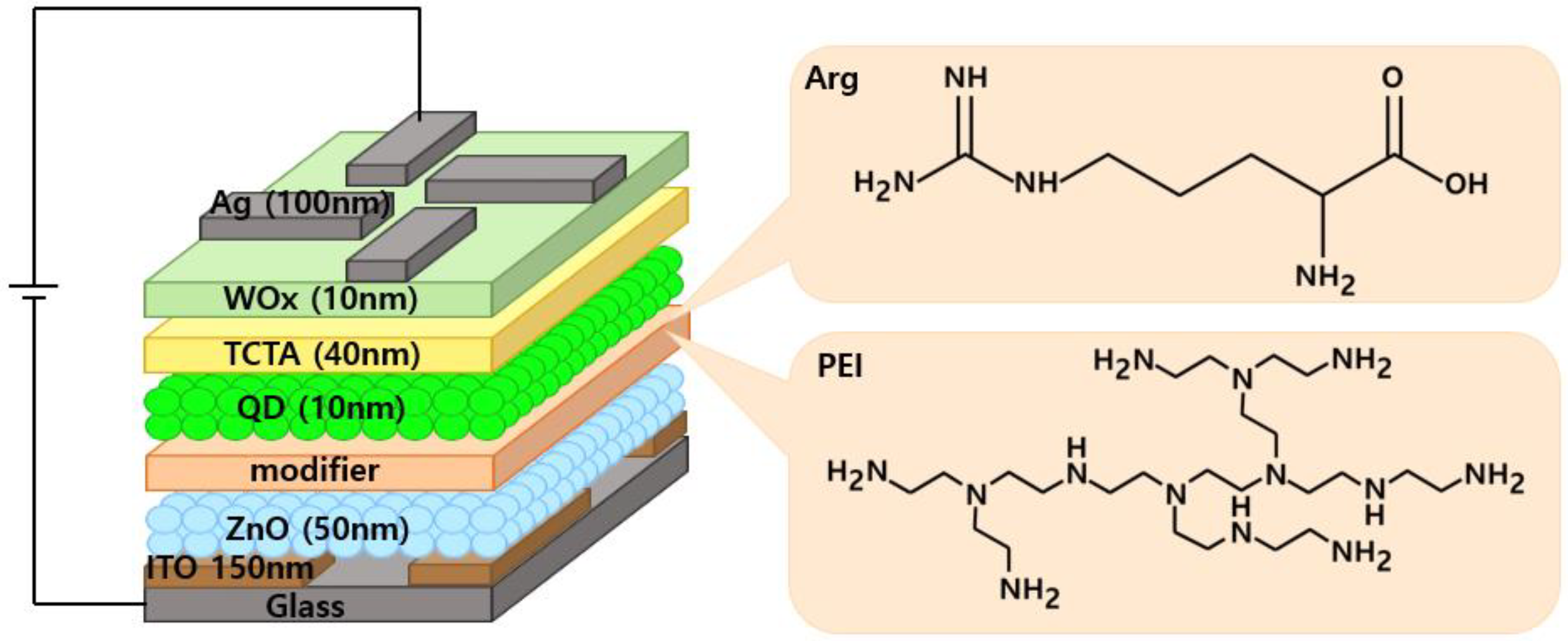
Figure 1.
Structure of the IQLEDs using Arg and PEI interlayers on ZnO NP layer and chemical structures of Arg and PEI.
Figure 1.
Structure of the IQLEDs using Arg and PEI interlayers on ZnO NP layer and chemical structures of Arg and PEI.
To assess the impact of the Arg on the device performance, IQLEDs were fabricated using different EILs of ZnO NPs (50 nm)/Arg (0 nm, 5 nm, 10 nm, 20 nm, 30 nm). Additionally, for comparative analysis, IQLEDs with EILs composed of ZnO NPs (50 nm)/PEI (5 nm) were fabricated.
Figure 1 presents the structures of IQLEDs with Arg and PEI ILs between QD EML and ITO/ZnO NP ETL and chemical structures of Arg and PEI. Control devices were established using ITO/ZnO NPs and ITO/ZnO NPs/PEI EILs.
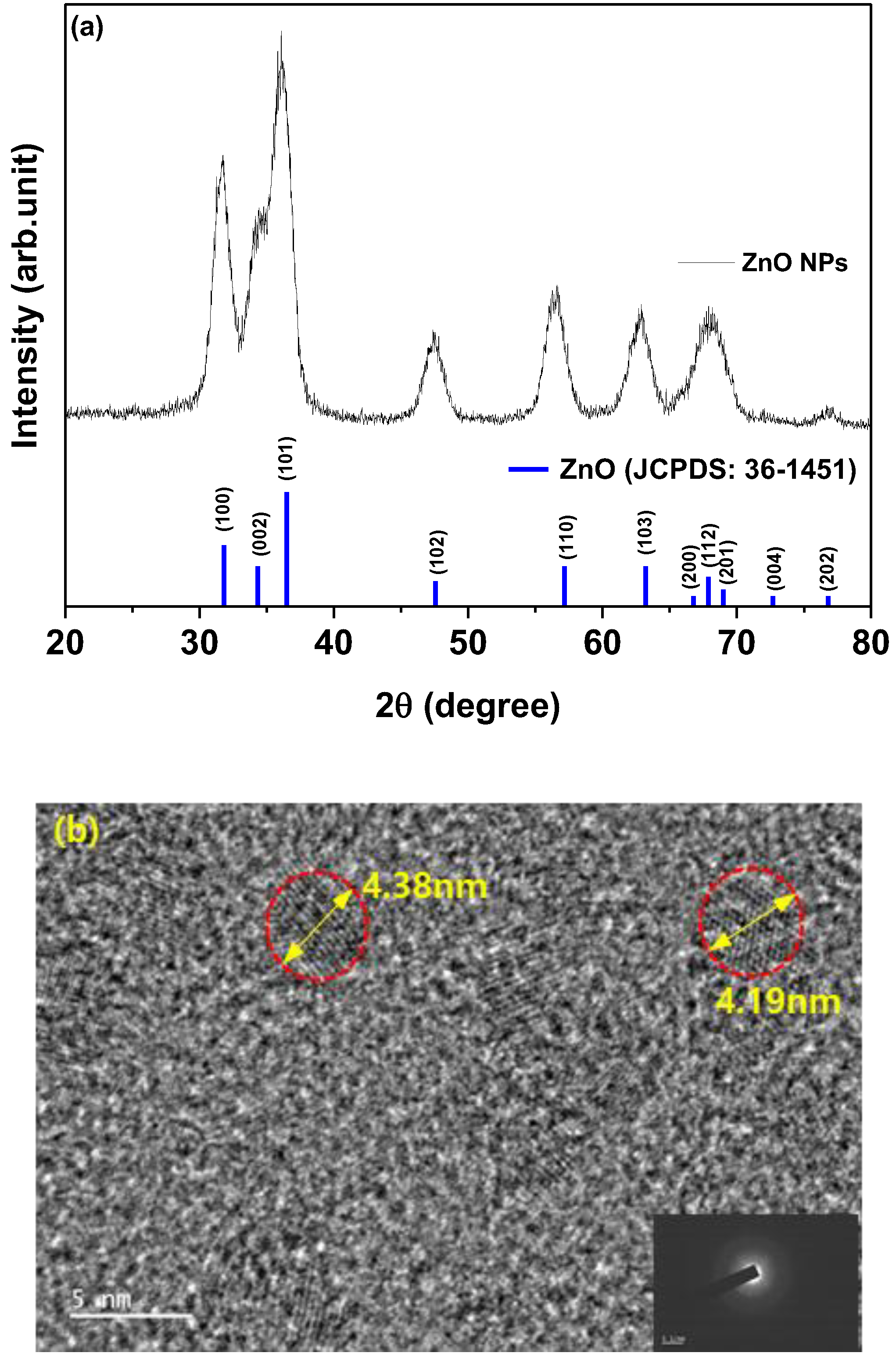
Figure 2(a) shows the characteristic 2θ XRD patterns of ZnO NPs, revealing the crystal structure. The crystal structure exhibited the characteristic hexagonal wurtzite pattern typical of ZnO (Joint Committee on Powder Diffraction Standards [JCPDS] Card 1-1136). XRD analysis of ZnO NPs revealed reflections in the (100), (002), (101), (102), (110), (103) and (112) planes, all corresponding to ZnO. Slight shifts in the diffraction peaks and intensities of ZnO NPs were observed, indicating minor lattice distortions and alterations in the interatomic spacing.
Figure 2(b) illustrates a representative FE-TEM image depicting ZnO NPs, with an average diameter measured at 4.29 nm.
Figure 2.
(a) X-ray diffraction patterns of ZnO nanoparticles over a 2θ range of 20–80° and (b) field-emission transmission electron microscopy of ZnO nanoparticles.
Figure 2.
(a) X-ray diffraction patterns of ZnO nanoparticles over a 2θ range of 20–80° and (b) field-emission transmission electron microscopy of ZnO nanoparticles.
Figure 3.
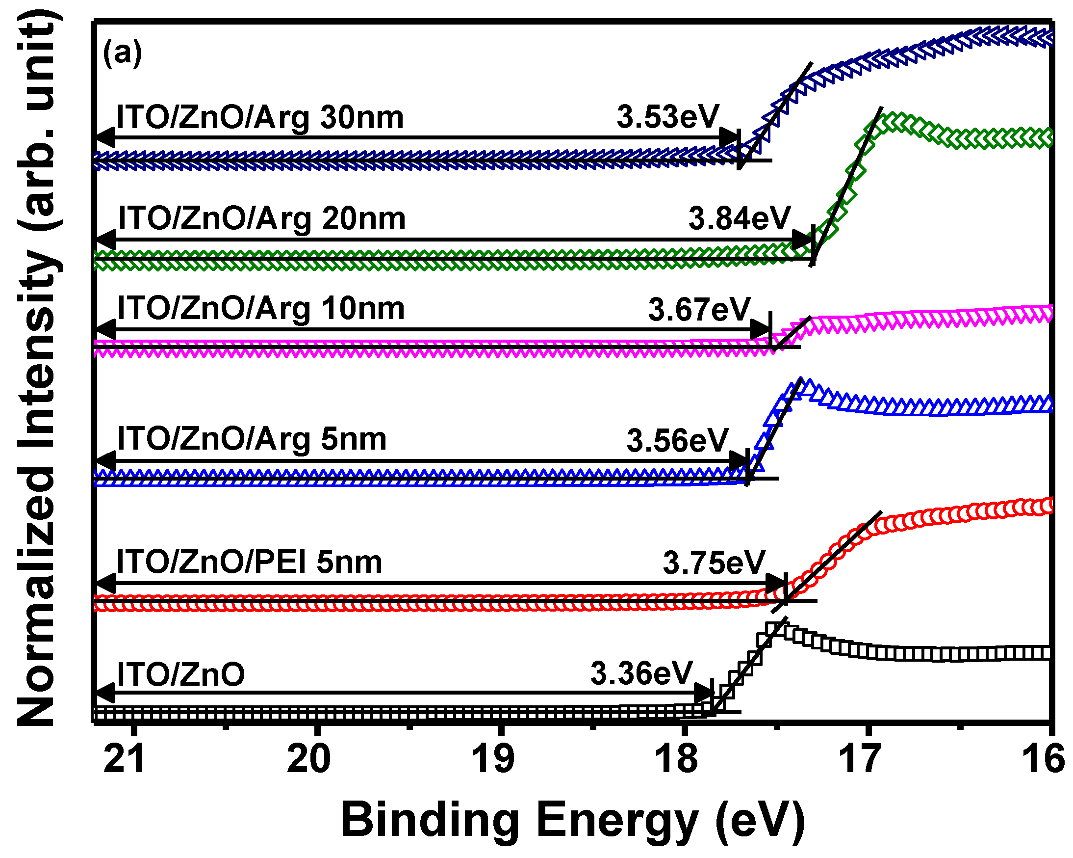
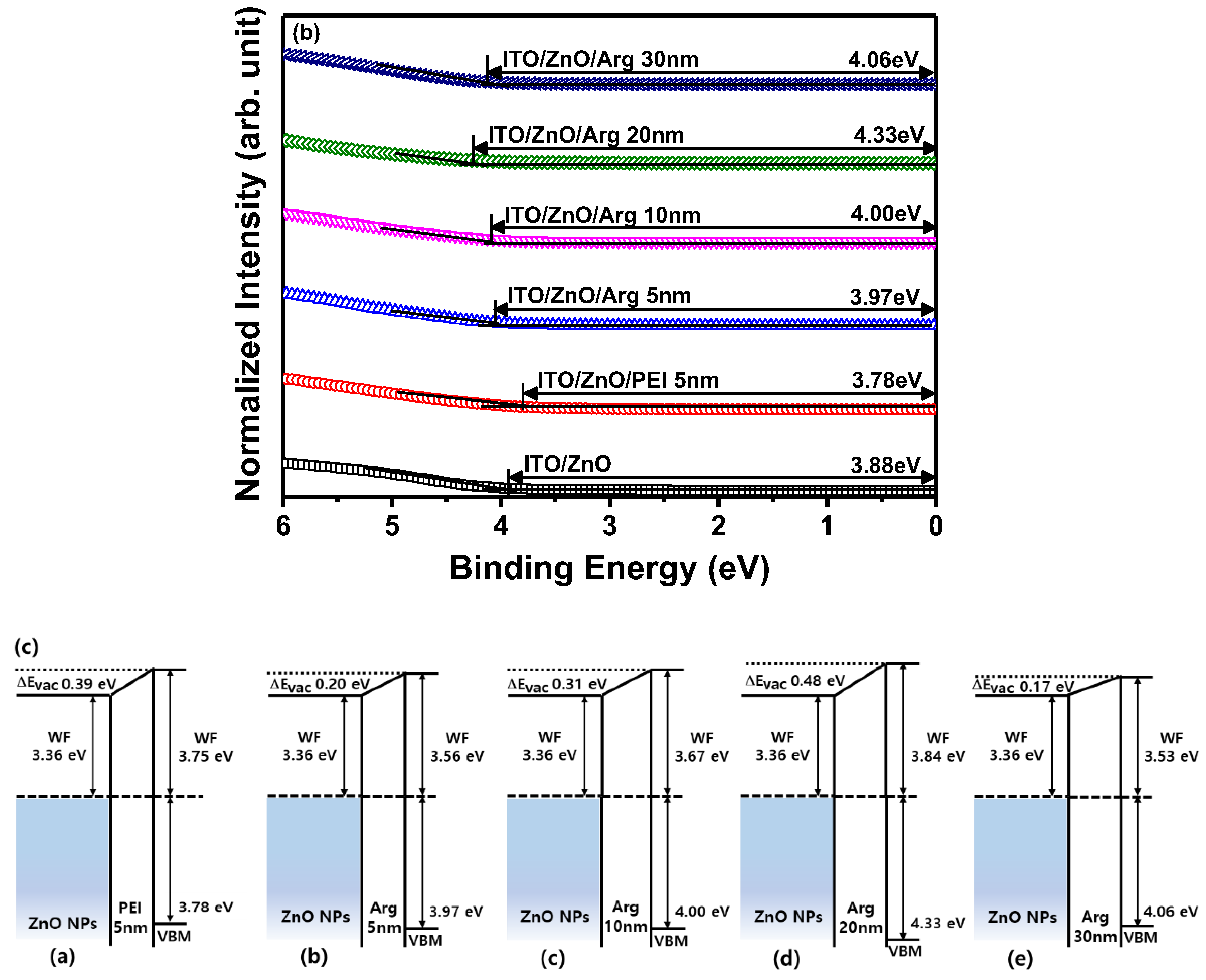
(a) Ultraviolet photoelectron spectroscopy spectra of secondary electron cut off regions, and (b) valence band regions of ITO/ZnO NPs, ITO/ZnO NPs/PEI (5 nm), ITO/ZnO NPs/Arg (5 nm), ITO/ZnO NPs/Arg (10 nm), ITO/ZnO NPs/Arg (20 nm), and ITO/ZnO NPs/Arg (30 nm). (c) Schematic energy level alignment diagrams of ZnO NPs/PEI (5 nm), ZnO NPs/Arg (5 nm), ZnO NPs/Arg (10 nm), ZnO NPs/Arg (20 nm), and ZnO NPs/Arg (30 nm).
To investigate the influence of Arg and PEI ILs on the work function variation of the ZnO NP EIL, UPS measurements were conducted. The electronic energy level configuration of thin films, specifically ITO/ZnO NPs, ITO/ZnO NPs/PEI (5 nm), ITO/ZnO NPs/Arg (5 nm), ITO/ZnO NPs/Arg (10 nm), ITO/ZnO NPs/Arg (20 nm), and ITO/ZnO NPs/Arg (30 nm), was examined using UPS. Figures 3(a) and (b) illustrates UPS spectra corresponding to the secondary-electron cutoff and valence band maximum regions. The estimated work functions below the vacuum level for the thin films are as follows: ITO/ZnO NPs (3.36 eV), ITO/ZnO NPs/PEI (5 nm) (3.75 eV), ITO/ZnO NPs/Arg (5 nm) (3.56 eV), ITO/ZnO NPs/Arg (10 nm) (3.67 eV), ITO/ZnO NPs/Arg (20 nm) (3.84 eV), and ITO/ZnO NPs/Arg (30 nm) (3.53 eV) eV). In
Figure 3(c), the electronic energy levels are illustrated, demonstrating shifts in work functions upon the insertion of ILs such as Arg and PEI between ZnO NP ETL and QD EML. The work functions of all samples containing Arg (5 nm, 10 nm, 20 nm, and 30 nm) and PEI ILs showed an increase compared to that of ITO/ZnO NPs. This indicates a rise in energy barriers for electron injection. When the PEI (5 nm) IL was coated onto the ZnO NP EIL, the work function increased more significantly compared to when the Arg IL (5 nm) was applied. The work function consistently increased with the increasing thickness of the Arg IL, except in the case where the thickness reached 30 nm. This trend suggests a potential decrease in the current density of the QLED as the thickness of the Arg IL increased.
Figure 4.
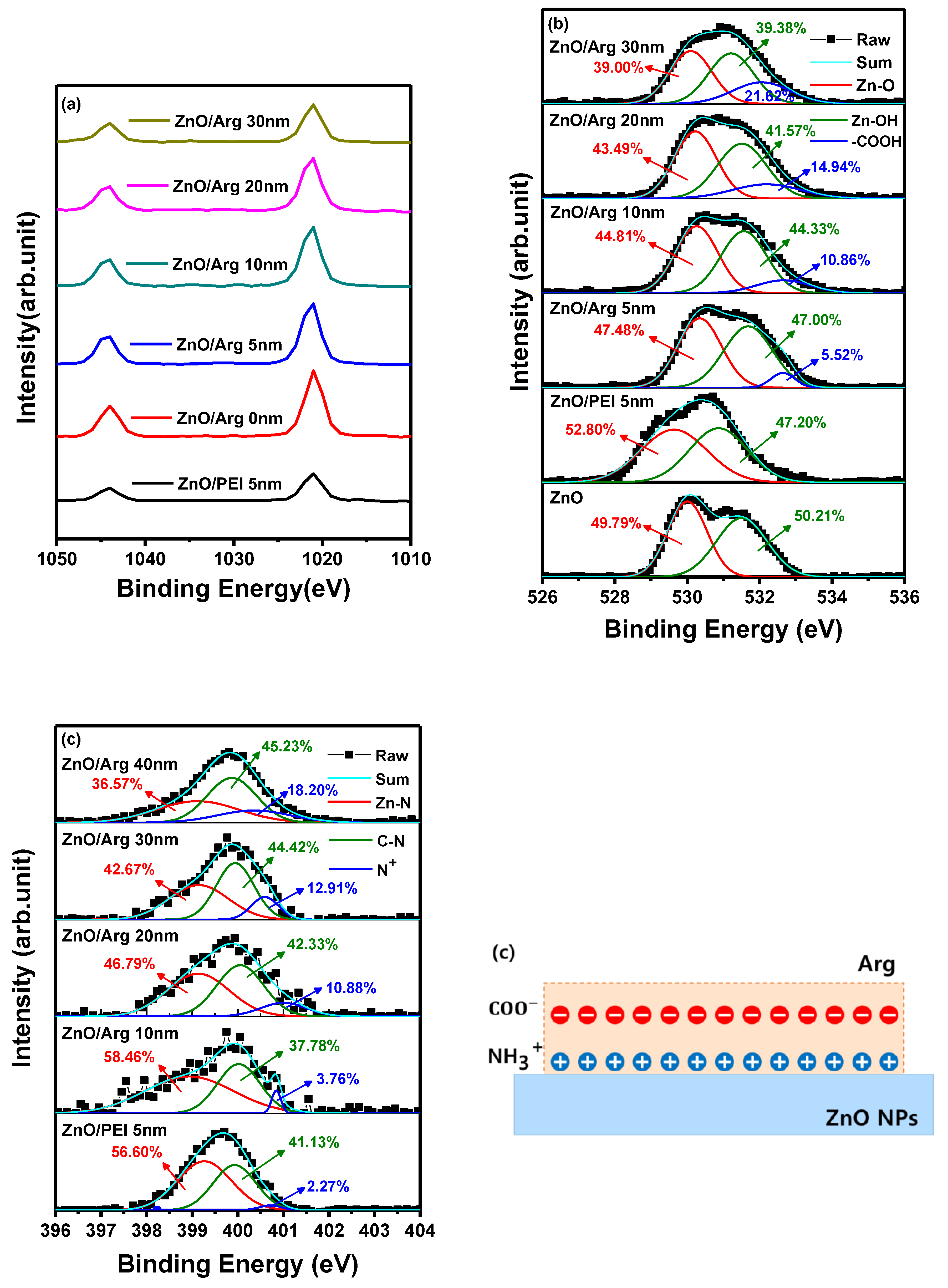
X-ray photoelectron spectroscopy spectra of ITO/ZnO NPs, ITO/ZnO NPs/PEI (5 nm), ITO/ZnO NPs/Arg (5 nm), ITO/ZnO NPs/Arg (10 nm), ITO/ZnO NPs/Arg (20 nm), and ITO/ZnO NPs/Arg (30 nm): (a) Zn 2p, (b) N 1s, and (c) O 1s. (d) Schematic of proposed physical model for creating an electrostatic dipole in Arg layer.
To enhance our comprehension of the molecular interaction between ZnO NPs and ILs (Arg and PEI), XPS measurements were performed. The analysis focused on the intensity of an interfacial dipole linked to protonated amines within a molecular layer, such as Arg and PEI [
31]. The objective was to investigate the influence of PEI (5 nm) and varying thickness of Arg (0 nm, 5 nm, 10 nm, 20 nm, and 30 nm) on ITO/ZnO substrates using XPS analysis.
Figure 4(a) shows Zn 2p peaks at 1043.97 eV and 1021.26 eV for ITO/ZnO NPs, 1043.97 eV and 1021.02 eV for ITO/ZnO NPs/PEI (5 nm), 1043.97 eV and 1021.75 eV for ITO/ZnO NPs/Arg (5 nm), 1043.97 eV and 1021.53 eV for ITO/ZnO NPs/Arg (10 nm), 1043.97 eV and 1021.57 eV for ITO/ZnO NPs/Arg (20 nm), and 1043.97 eV and 1021.41 eV for ITO/ZnO NPs/Arg (30 nm). The energy differences of 22.71 eV for ITO/ZnO NPs, 22.95 eV for ITO/ZnO NPs/PEI (5 nm), 22.22 eV for ITO/ZnO NPs/Arg (5 nm), 22.44 eV for ITO/ZnO NPs/Arg (10 nm), 22.40 eV for ITO/ZnO NPs/Arg (20 nm), and 22.56 eV for ITO/ZnO NPs/Arg (30 nm) between two peaks indicate a normal chemical state of Zn2+ for the compounds [
31,
33]. In comparison with the ZnO NPs, the binding energy location for the PEI-modified ZnO NPs slightly decrease, but Arg-modified ZnO increases, indicating that the electronic structure of ZnO is influenced by the formation of the Zn−N chemical bonding [
31].
Figure 4(b) shows that the N 1s peaks in the films consisted of ITO/ZnO NPs/PEI (5 nm), ITO/ZnO NPs/Arg (5 nm), ITO/ZnO NPs/Arg (10 nm), ITO/ZnO NPs/Arg (20 nm), and ITO/ZnO NPs/Arg (30 nm) thin films. The thin films exhibited an asymmetric N 1s spectra. The spectra were deconvoluted into three binding states, attributed to nitrogen bonded to Zn in the metal oxide lattice, the nitrogen atoms in the neutral amines, and the nitrogen atoms in protonated amines. The high resolution XPS spectra of N 1s exhibited three asymmetric peaks at 399.25 eV, 399.98 eV and 400.79 eV for ITO/ZnO NPs/PEI (5 nm) film, at 398.98 eV, 399.98 eV, and 400.79 eV for ITO/ZnO NPs/Arg (5nm) film, at 399.46 eV, 399.91 eV, and 400.13 eV for ITO/ZnO NPs/Arg (10 nm) film, at 399.21 eV, 399.95 eV, and 400.39 eV for ITO/ZnO NPs/Arg (20 nm) film, and at 399.14 eV, 399.77 eV, and 400.12 eV for ITO/ZnO NPs/Arg (30 nm) film as shown in
Figure 4(b). The presence of protonated amines, known for inducing electrostatic dipoles [
29,
34], is responsible for the intensity of an interfacial dipole. In all samples coated with Arg and PEI ILs, distinct features were observed: C 1s peaks near 286 eV and nitrogen 1s peaks that corresponding to protonated amines (slightly higher than 400 eV) and non-protonated amines (slightly less than 400 eV). The concentration of protonated nitrogen (N+) in the following structures-ITO/ZnO NPs/PEI (5 nm), ITO/ZnO NPs/Arg (5 nm), ITO/ZnO NPs/Arg (10 nm), ITO/ZnO NPs/Arg (20 nm), and ITO/ZnO NPs/Arg (30 nm)-were calculated as 2.27%, 3.76% 10.88%, 12.91%, and 18.20%, respectively. Additionally, the O 1s peaks for thin films of ITO/ZnO NPs and their respective combinations-ITO/ZnO NPs/PEI (5 nm), ITO/ZnO NPs/Arg (5 nm), ITO/ZnO NPs/Arg (10 nm), ITO/ZnO NPs/Arg (20 nm), and ITO/ZnO NPs/Arg (30 nm)-were estimated to be 530.26 eV, 530.99 eV, 530.55 eV, 530.53 eV, 530.87 eV, and 530.91 eV, respectively, as shown in
Figure 4(c). When utilizing the ILs, a reduction in the hydroxyl group ratio occurs due to the substitution of these groups in Arg. It appears that the amine groups in Arg replaced more hydroxyl groups compared to those in PEI. Furthermore, with increasing Arg thickness, there was a decrease in the hydroxyl group ratio and an increase in the carboxyl group ratio, as shown in
Figure 4(c). The carboxyl group has ability to donate a proton (H+) in a chemical reaction, while the amine group, containing nitrogen, acts as a base by accepting protons. The protonated amine groups align in proximity to the surface of ZnO NPs, whereas the negatively charged carboxyl groups are externally positioned on Arg IL. This configuration gives rise to the creation of electrostatic dipoles [
35,
36]. When these dipoles are aligned perpendicularly to the surface and directed inward, their formation results in an increase in the work function, illustrated in
Figure 4(d). This correlation was confirmed by the UPS results.
Figure 4(d) presents a physical model proposed based on the properties of Arg.
Figure 5.
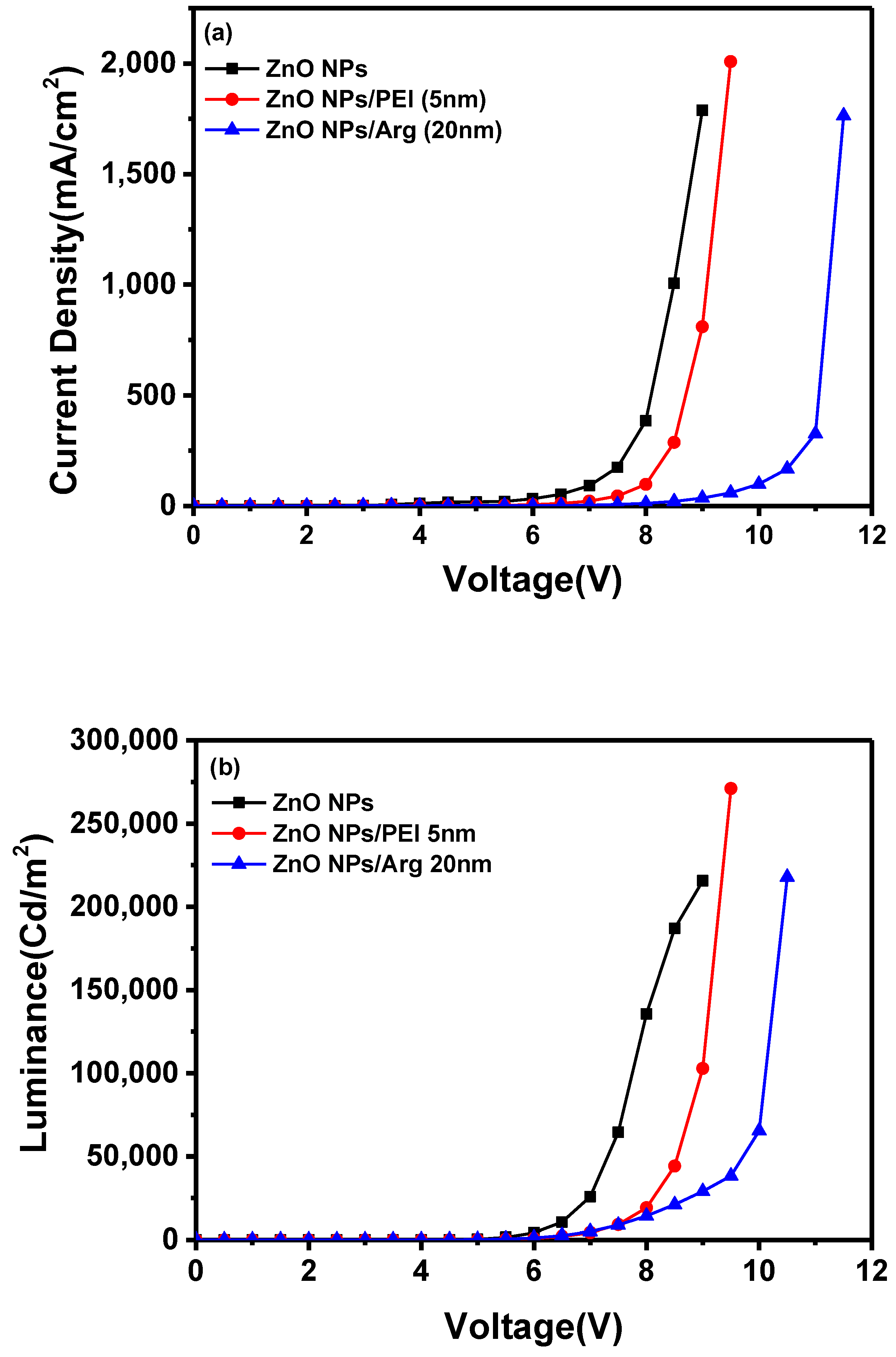
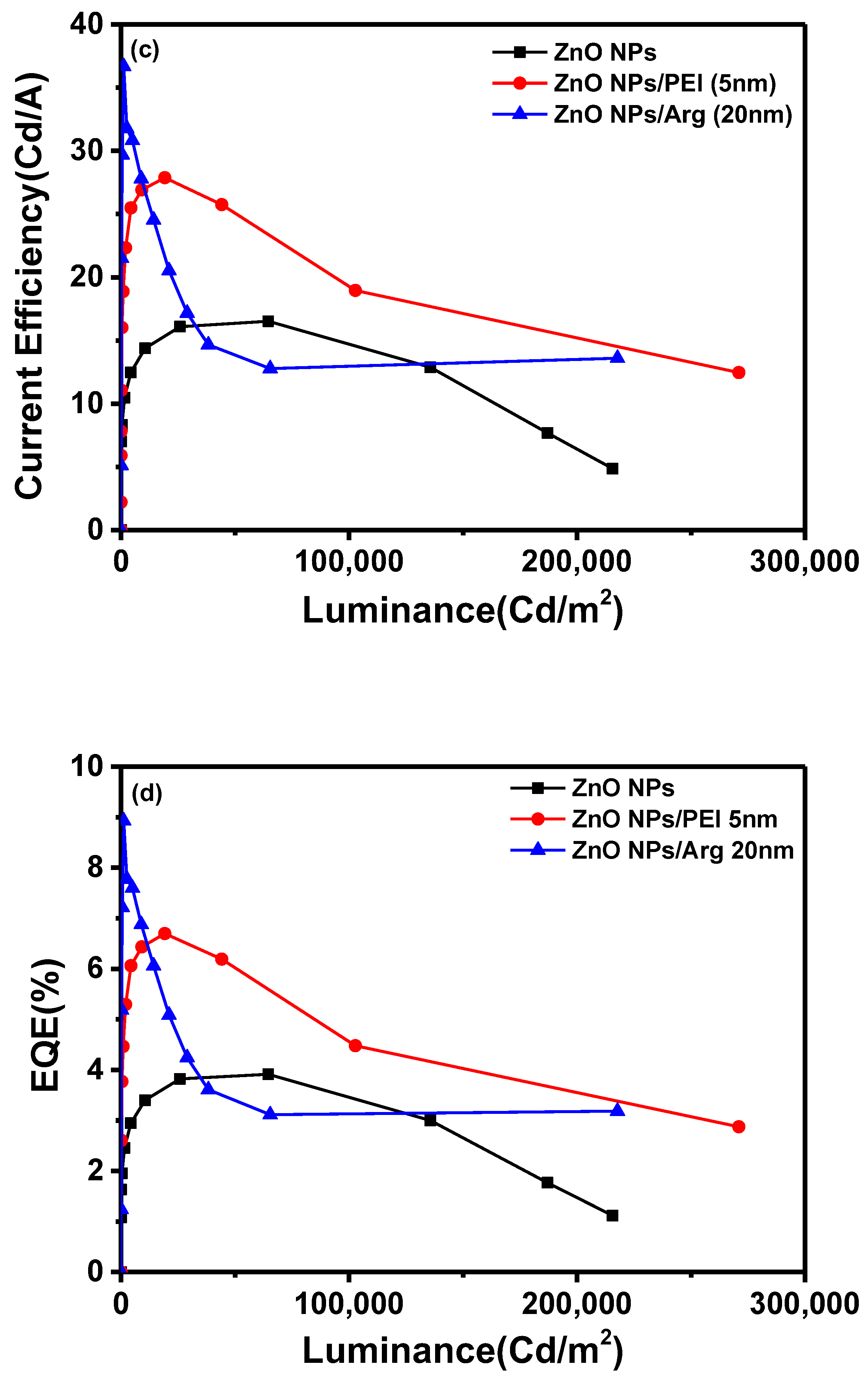
Electroluminescence (EL) characteristics of IQLEDs with ZnO NPs, ZnO NPs/Arg (20 nm), and ZnO NPs/PEI (5 nm) electron injection layers: (a) current density-voltage curves, (b) luminance-voltage curves, (c) current efficiency-luminance curves, and (d) external quantum efficiency-luminance curves.
With the increased energy barriers for electron injection in IQLEDs with PEI and Arg ILs on ZnO NP EIL, it is expected that the current density for IQLEDs should decrease. To compare the effect of the Arg and PEI ILs, we fabricated IQLEDs using ZnO (20 nm), ZnO (20 nm)/PEI (5 nm), and ZnO (20 nm)/Arg (20 nm) EILs. The electroluminescence (EL) characteristics of these IQLEDs are illustrated in
Figure 5. Our findings revealed a decrease in current density decreased upon integration of the Arg and PEI ILs on ZnO NPs, indicating reduced electron injection compared to IQLEDs with ZnO NPs. It is believed that the decrease in current density is attributed to the increased energy barriers for electron injection, combining with the inherent insulating nature of the ILs. As illustrated in
Figure 5(a), the IQLED with a 20-nm-thick Arg IL demonstrated a more substantial reduction in current density compared to the IQLED with a 5-nm-thick PEI IL. Despite Arg exhibiting lower barriers for electron injection compared to PEI IL, it demonstrated a lower current density, indicating higher insulating nature than PEI. The luminance values of IQLEDs followed similar trends as the current density. While the maximum current efficiencies of IQLEDs with ZnO, ZnO/PEI, and ZnO/Arg EILs were estimated to be 16.51 cd/A, 27.33 cd/A, and 36.67 cd/A, respectively, the EQEs of these IQLEDs were determined to be 3.91%, 6.56%, and 8.93%, respectively. IQLED with ZnO NPs/Arg (20 nm) EIL exhibited a 2.22-fold higher current efficiency and a 2.28-fold higher EQE compared to IQLED with ZnO NPs EIL, and it demonstrated a 1.34-fold higher current efficiency and a 1.36-fold higher EQE compared to IQLED with ZnO NPs/PEI (5 nm) EIL. Despite having the lowest current density, QLED with Arg (20nm) IL exhibited the highest maximum current efficiency and EQE. This could be attributed to the highest charge balance achieved in the QD EML and minimized exciton quenching according to the low concentration of hydroxyl groups, as confirmed by XPS analysis, thereby enhancing luminance [
2,
25,
37]. The key parameters of IQLEDs with ZnO NPs, ZnO NPs/PEI (5 nm), and ZnO NPs/Arg (20 nm) are summarized in
Table 1.
Figure 6.
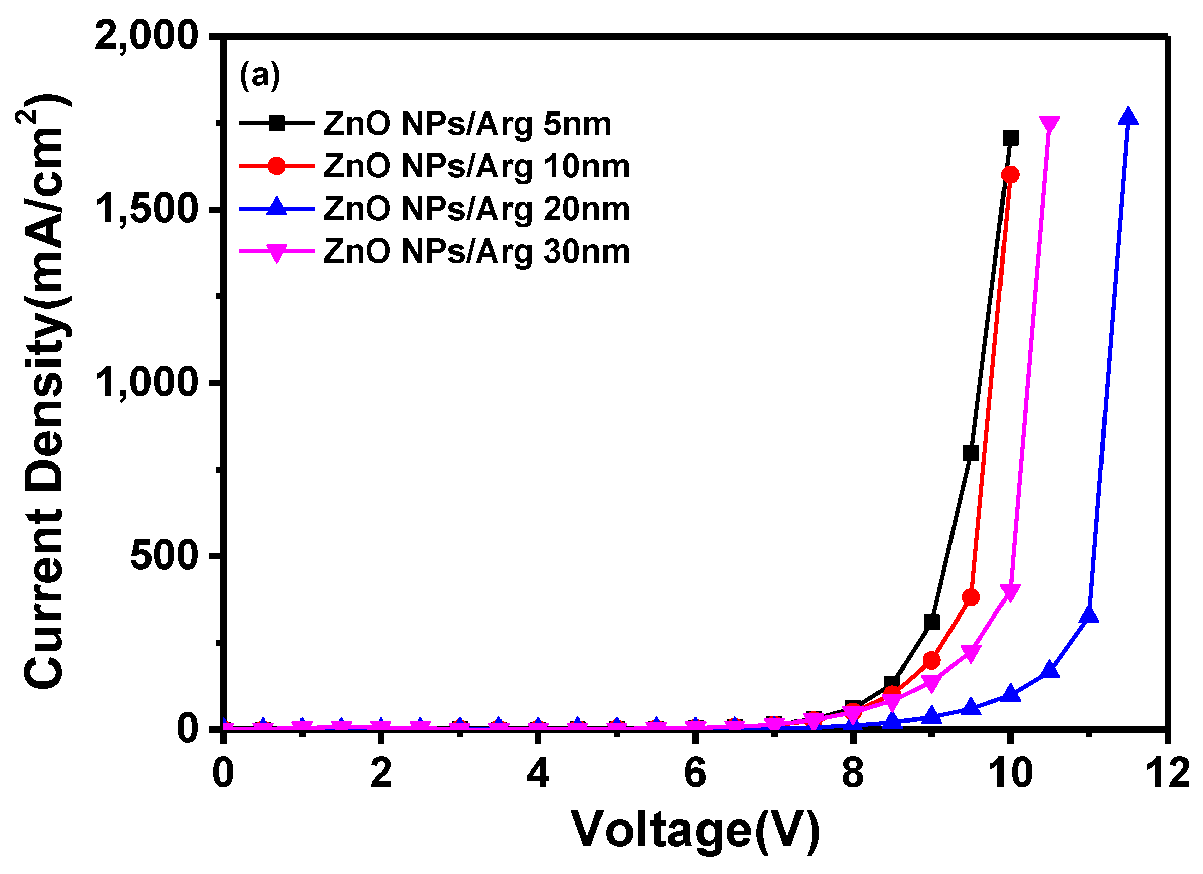
Electroluminescence (EL) characteristics of QLEDs with ZnO NPs/Arg (50 nm), ZnO NPs/Arg (10 nm), ZnO NPs/Arg (20 nm), and ZnO NPs/Arg (30 nm: (a) current density-voltage curves, (b) luminance-voltage curves, (c) current efficiency-luminance curves, and (d) external quantum efficiency-luminance curves.
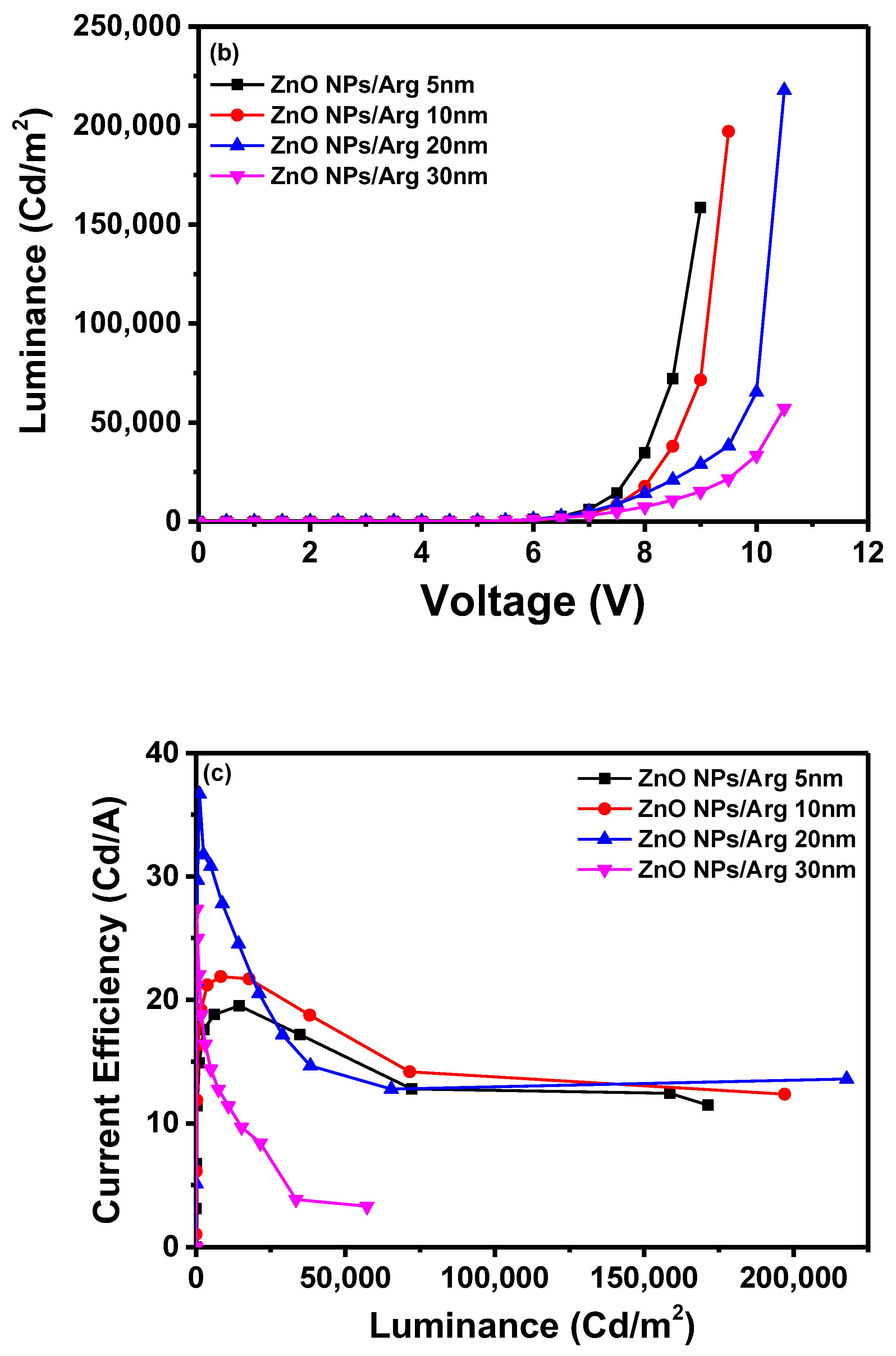
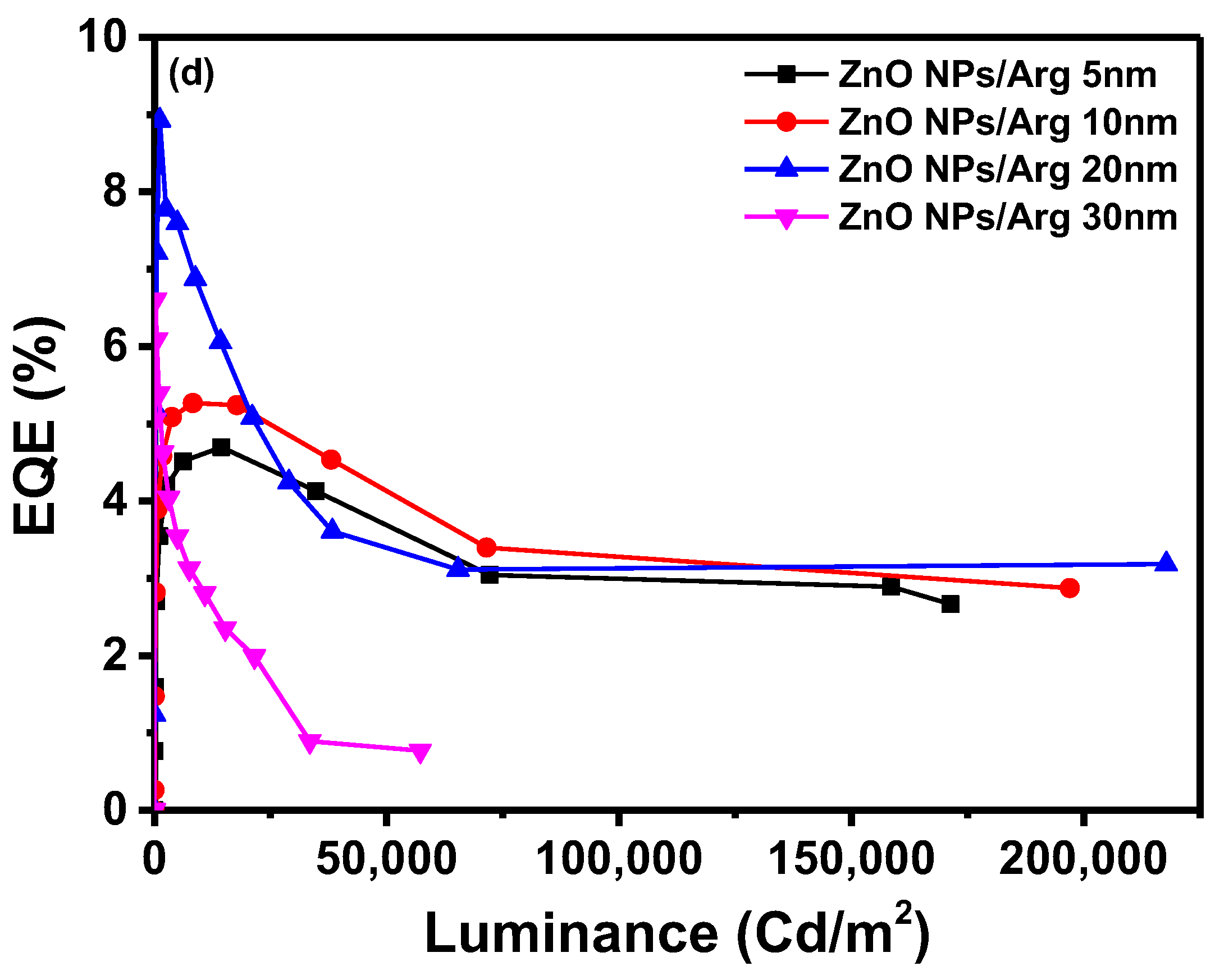
To evaluate the effects of varying Arg IL thicknesses, IQLEDs were fabricated using Arg ILs of varying thicknesses (5 nm, 10 nm, 20 nm, and 30 nm). In
Figure 6, the EL characteristics of these IQLEDs are illustrated. In
Figure 6(a), the plotted current density curves against applied voltage clearly depict a trend: as the thickness of the Arg IL increased, the current density of the IQLEDs decreased. Interestingly, although the IQLED with a 30 nm thickness of Arg IL showed lower current density compared to the one 20 nm thickness, despite having lower energy barriers for electron injection. This suggests that the dominant influence is driven by the inherent insulating nature rather than the effect of energy barriers. Additionally, the maximum luminance values of IQLEDs with varying Arg IL thicknesses were estimated as follows:158,567.8 cd/m
2 for IQLED with 5-nm-thick Arg IL, 197,017.8 cd/m
2 for IQLED with 10-nm-thick Arg IL, 217,780.8 cd/m
2 for IQLED with 20-nm-thick Arg IL, and 57,228.9 cd/m
2 for QLED with 30-nm-thick Arg IL. Among these, the IQLED with a 20-nm-thick Arg IL exhibited the highest luminance, indicating the optimal charge balance within the QD EML. Moreover, the reduced direct contact between the QD EML and ZnO NP EIL, facilitated by the inherent insulating properties of Arg, combined with the decreased concentration of hydroxy groups in ZnO NPs, is believed to have minimized exciton quenching, resulting in the highest luminance [
2,
25]
Figure 6(c) illustrates the maximum current efficiencies of IQLEDs with Arg ILs with thicknesses of 5 nm, 10 nm, 20 nm, and 30 nm, measuring at 19.53 cd/A, 21.89 cd/A, 36.67 cd/A, and 27.35 cd/A, respectively. Similarly, the maximum EQEs for these IQLEDs with 5-nm-thick, 10-nm-thick, 20-nm-thick, and 30-nm-thick Arg ILs were calculated at 4.7%, 5.27%, 8.93%, and 6.61%, respectively. We believe that current efficiency and EQE are influenced by the charge balance within the QD EML and the exciton quenching at the interface between the QD EML and the Arg IL. As a result, the IQLED with 20-nm-thick Arg IL exhibits a 2.28 times improvement in EQE compared to IQLED without an IL, while the IQLED with a 20-nm-thick Arg IL shows a 1.36 times improvement in EQE compared to IQLED with a 5-nm-thick PEI IL.
Table 2 summarizes the key parameters of TE-QLEDs with ZnO NPs/Arg (5 nm), ZnO NPs/Arg (10 nm), ZnO NPs/Arg (20 nm), and ZnO NPs/Arg (30 nm) EILs.
Figure 7.
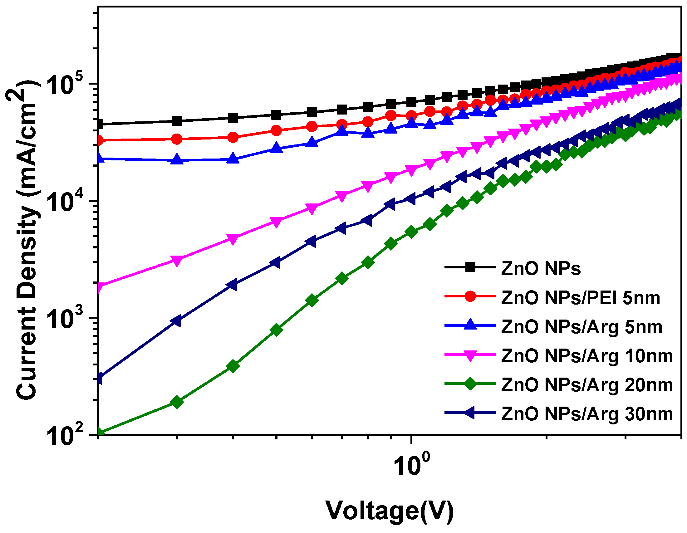
Comparison of the current density curves as an applied voltage for electron only devices, ITO (150nm)/ZnO NPs (50 nm)/Arg (0 nm, 5 nm, 10 nm, 20 nm, 30 nm) and PEI (5 nm)/QD (10 nm)/Ag (100 nm).
Figure 7.
Comparison of the current density curves as an applied voltage for electron only devices, ITO (150nm)/ZnO NPs (50 nm)/Arg (0 nm, 5 nm, 10 nm, 20 nm, 30 nm) and PEI (5 nm)/QD (10 nm)/Ag (100 nm).
To further explore the effect of Arg on electron injection, we fabricate the electron-only devices (EODs). We developed six EOD variants with different Arg thicknesses (0 nm, 5 nm, 10 nm, 20 nm, 30 nm) and PEI (5 nm). The structures of the EODs consisted of ITO (150nm)/ZnO NPs (50 nm)/Arg (5 nm, 10 nm, 20 nm, 30 nm) and PEI (5 nm)/QD (10nm)/Ag (100 nm). Electrons injection occurred from the cathode to the conduction band minimum (CBM) level of QDs via the CBM of ZnO NPs/Arg EILs. Comparing the current densities of EOD using Arg ILs with varying thicknesses were smaller than those of EODs with ZnO NPs and ZnO NPs/PEI (5 nm) ILs, we observed that, except for EOD with 30-nm-thick Arg, the energy barriers for electron injection in EODs with varying thicknesses of Arg ILs were higher than those of EODs with ZnO NPs and ZnO NPs/PEI ILs. This suggests that the insulating nature of Arg surpasses that of PEI. An EOD with a 30-nm-thick Arg exhibited a lower barrier for electron injection compared to the EOD with a 10-nm-thick Arg, indicating that the EOD with a 30-nm-thick Arg is more influenced by its inherent insulating nature than the effect of the energy barrier.
Figure 7.
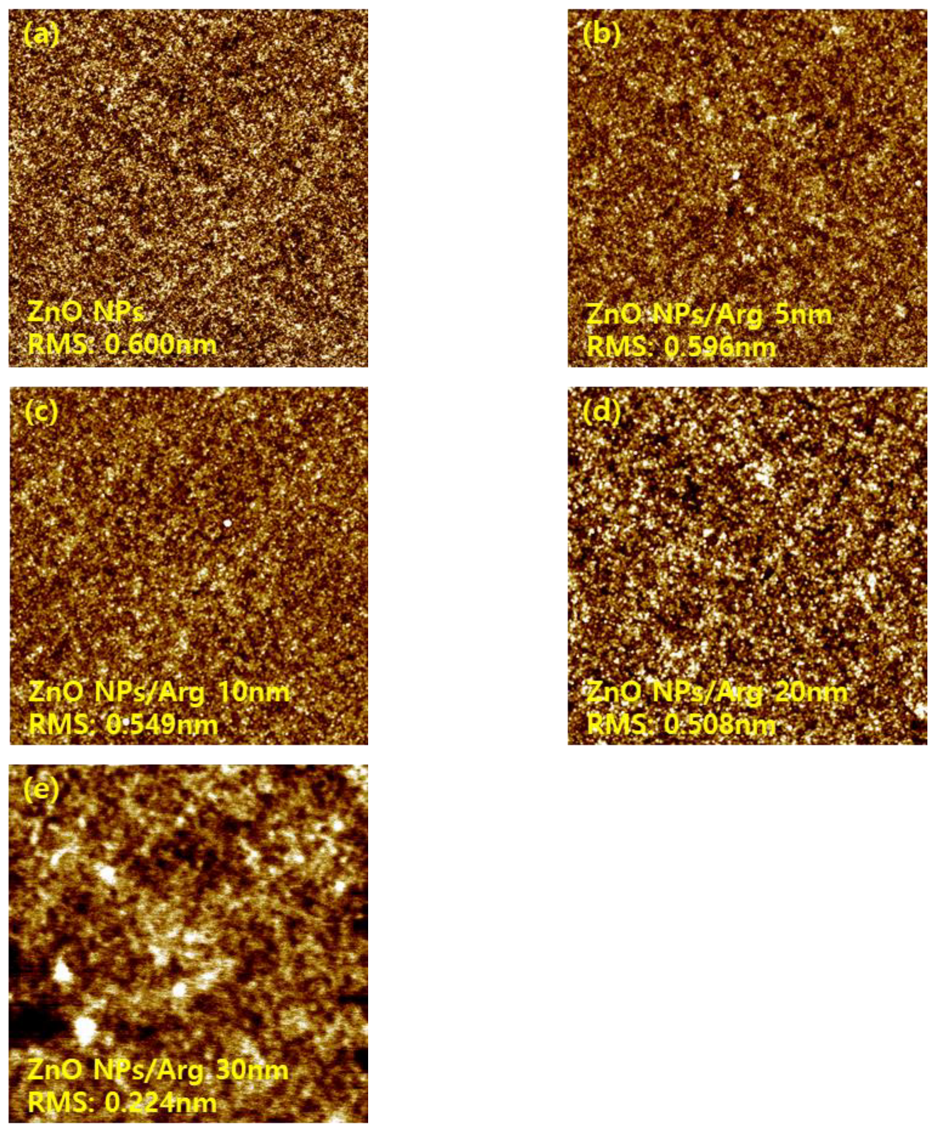
Atomic force microscope images of ZnO NPs, ZnO NPs/Arg (5 nm), ZnO NPs/Arg (10 nm), ZnO NPs/Arg (20 nm), and ZnO NPs/Arg (30 nm) films.
Figure 7.
Atomic force microscope images of ZnO NPs, ZnO NPs/Arg (5 nm), ZnO NPs/Arg (10 nm), ZnO NPs/Arg (20 nm), and ZnO NPs/Arg (30 nm) films.
Surface morphology properties of the ITO/ZnO NPs and ITO/ZnO NPs/Arg ILs (5nm, 10 nm, 20 nm, and 30 nm) were characterized via AFM measurements, and the results are presented in Figure 7. The ITO/ZnO NP film exhibited the largest roughness, with a root-mean-square (RMS) value of 0.600 nm. Upon the application of Arg and PEI ILs on the ZnO NP surface, smoother surfaces were observed, indicating complete coverage by Arg and PEI ILs. This suggests that as the thickness of the Arg increased, the reduced surface roughness was attributed to replacement of more hydroxyl groups on the ZnO NPs with more amine groups in the Arg molecule. Interestingly, applying Arg on the ZnO NP surface resulted in a rougher surface compared to when PEI was used. This might be attributed to Arg molecules, which align perpendicularly to the ZnO NP surface, contrasting with the horizontal application of PEI, as reported by Li et al. [
31].
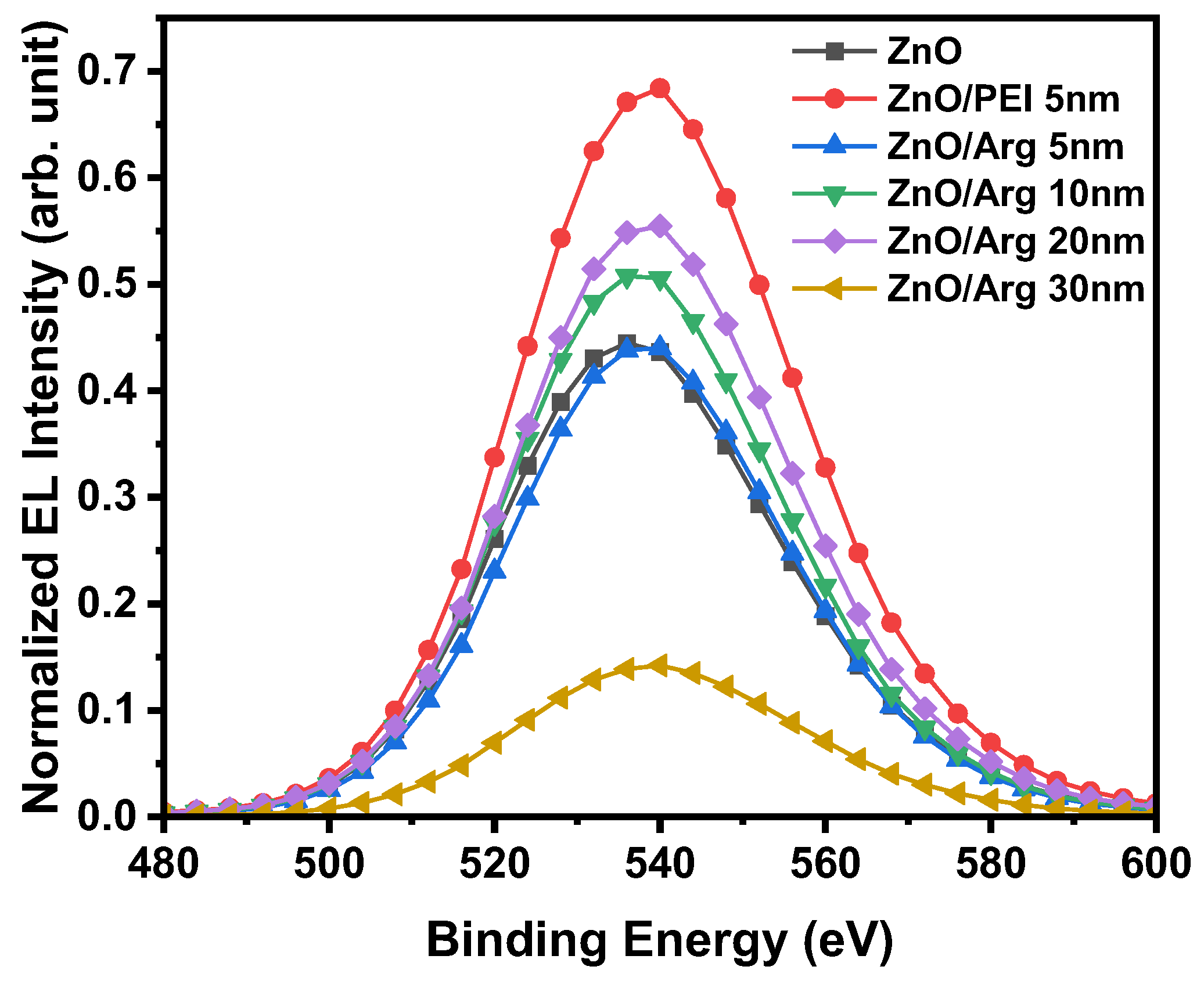
Figure 8 shows the normalized electroluminescence spectra of IQLEDs with ZnO NPs, ZnO NPs/PEI (5nm), ZnO NPs/Arg (5 nm), ZnO NPs/Arg (10 nm), ZnO NPs/Arg (20 nm), and ZnO NPs/Arg (30 nm) at the applied voltage for maximum luminescence. All the devices with different EILs showed the same peak position at 540 nm. The full width at half maximum values of the IQLEDs with ZnO NPs, ZnO NPs/PEI (5nm), ZnO NPs/Arg (5 nm), ZnO NPs/Arg (10 nm), ZnO NPs/Arg (20 nm), ZnO NPs/Arg (30 nm) at the point of maximum luminance, were estimated to be 39.9 nm, 39.7 nm, 39.0 nm, 38.9 nm, 39.3 nm, and 40.3 nm, respectively. The IQLED with a ZnO NPs/PEI IL demonstrated the highest emission peak, surpassing those of the QLEDs using any Arg ILs. The comprehensive characteristic parameters are summarized in
Table 3.
