1. Introduction
Logic- or binary-based computing machines currently experience enormous challenges due to reliability and thermal problems. Binary systems have demonstrated inevitable limitations due to the demands for extremely high-speed data processing and storage[
1,
2]. Multiple valued logic (MVL) has gained attention in the area of memory devices, computing, and other related applications. Unlike the Boolean logic system, the MVL system consists of digits, whereby each digit can have three or more values, which offers less circuit complexity and high information density. Similarly, circuit overhead, area, and energy consumption are reduced in the MVL system. Although there are different types of multiple-valued logic, the ternary logic system has been extensively studied over the last decade because it is the most feasible, simple, and easy to implement with nano-dimensional devices [
3,
4,
5,
6]. In unbalanced ternary logic, the logic levels 0, 1, and 2 are considered low, middle, and high states, respectively [
7]. As highlighted earlier, the three-state system has several advantages in logic design or digital systems. For instance, both binary and ternary logic gates can generate a y-valued logic function f(x) of n variables. The possible functions from both systems are
(16) and
(729), respectively, where n is the number of logic states. This shows ternary logic can provide more functionality and dense implementation with lower cost and area. Ternary logic can be realized with multi-threshold devices such as 2D transistors and memristors[
8,
9].
A memristor in its pristine form does not require extra hardware to handle multiple states that are further quantized into different levels. It is a very small-dimensional device (2 – 10) nm and compatible with standard CMOS process technology. Several studies have highlighted the importance of memristors in logic gates. Memristor was employed for computation in the design of standalone and hybrid memristor-CMOS logic [
10,
11]. Cho et al. [
12] proposed memristor ratioed logic (MRL), which occupies less die area as compared to CMOS. However, a fully memristor-based inverter cannot be implemented, so a CMOS inverter is required to invert and restore signals. Memristor-aided logic (MAGIC) is comprised of two sequential stages and was used to define logic states (0 and 1) using the low (R
on) and high (R
off) resistance states of the input and output memristors. Kvatinsky et al. introduced a more realistic threshold voltage based VTEAM memristor to implement MAGIC[
13]. In addition to AND, OR, and NOR Whitehead and Russell presented material implication (IMPLY) gate logic states defined by resistance instead of current and voltage across the memristor[
14]. Lastly, a memristor is a good replacement in ternary circuits to achieve multiple voltage levels.
Novel devices such as 1D and 2D transistors are being explored in MVL to overcome a few problems such as channel effects, drain-induced barrier lowering (DIBL), scaling limitations, etc.[
15]. The threshold voltage (V
th) of these devices can be easily altered, which offers a great benefit to logic circuit. For example, V
th of graphene nanoribbon field-effect transistor (GNRFET)[
16] and carbon nanotube field-effect transistor (CNTFET) by using ribbons with different width and tubes of different diameter, respectively. Negative, positive, and standard ternary inverters are designed in ref. [
8], but the limitation of the design is the large value resistance that dissipates excessive power. Various designs of ternary and quaternary logic using GNRFET have been implemented [
17,
18]. However, the circuits are too complex and occupy a large silicon area. Similarly, Lin et al. introduced CNTFET-based ternary logic, multiplier circuits, and half adders, and evaluated their performance over resistive-load CNTFET logic[
19]
This study presents ternary logic gates composed of hybrid memristor-2D transistors and conducts performance comparisons on them. A concise overview of memristors and their key characteristics is provided. Using GNRFET, MoS2 FET, WSe2 FET, and FinFET, a memristor-based standard ternary inverter (STI) is designed and its performance metrics, including delay, power, and energy delay product (EDP), are evaluated. An assortment of TMDC-based and graphene transistors are analyzed and subsequently integrated with memristors in order to fabricate NAND, inverter, and NOR gates. Furthermore, an analysis is conducted on the power, delay, EDP, VTC curve, and power of the inverter for each transistor technology. In addition, additional logic gates, including AND, NOR, OR, and NAND, were simulated using the T-SPICE EDA tool; the outcomes and truth table exhibit a strong concurrence.
2. Memristor
Leon Chua introduced the memristor as the fourth essential component of electrical circuits in 1971 [
20]. Later, the idea was expanded to include a class of dynamical systems known as memristive devices [
21]. More specifically, Chua pointed out that the four fundamental circuit variables—electric current (i), voltage (v), charge (q), and magnetic flux (Φ)—are connected in pairs by six different mathematical relations. The definitions of two of the variables can be used to derive one of these relationships (the charge is the time integral of the current), and Faraday’s rule of induction can be used to determine another relationship (the flux is the time integral of the electromotive force, or voltage). As a result, the remaining relationships between the variables should define four fundamental circuit parts. The memristor, which has memristance M, is the ‘missing’ component that gives the functional relationship between charge and flux, dΦ = Mdq.
Practically, the most widely used methods for fabricating memristor are nano-imprint lithography (NIL) and atomic layer deposition (ALD). Both methods require expensive equipment and multiple fabrication steps including a high temperature annealing step and a “forming” step. Other several methods of fabrications have been proposed such as electrohydrodynamic inkjet printing technology [
22] or the conventional photolithography technology [
23,
24]. A nonvolatile nanoscale TiO
2 device with synaptic properties was recently created by the Stanley Williams group at HP [
25].
Due to the great properties of the memristor for both memory and neuromorphic applications, interest in them has recently increased tremendously [
26,
27,
28]. However, the lack of a physical device that can implement the architecture of an integrated storage and computing system has slowed down its development over the past few decades. It is nonvolatile and only a few nanometers in size, which makes it ideal for memory applications.
A good understanding of metal oxide-based memristors, their operations and modelling are presented in this section. Earlier studies have demonstrated the use of binary oxides, perovskites, organics, common and special electrodes as resistive switching materials for memristor. For instance, HP memristor in
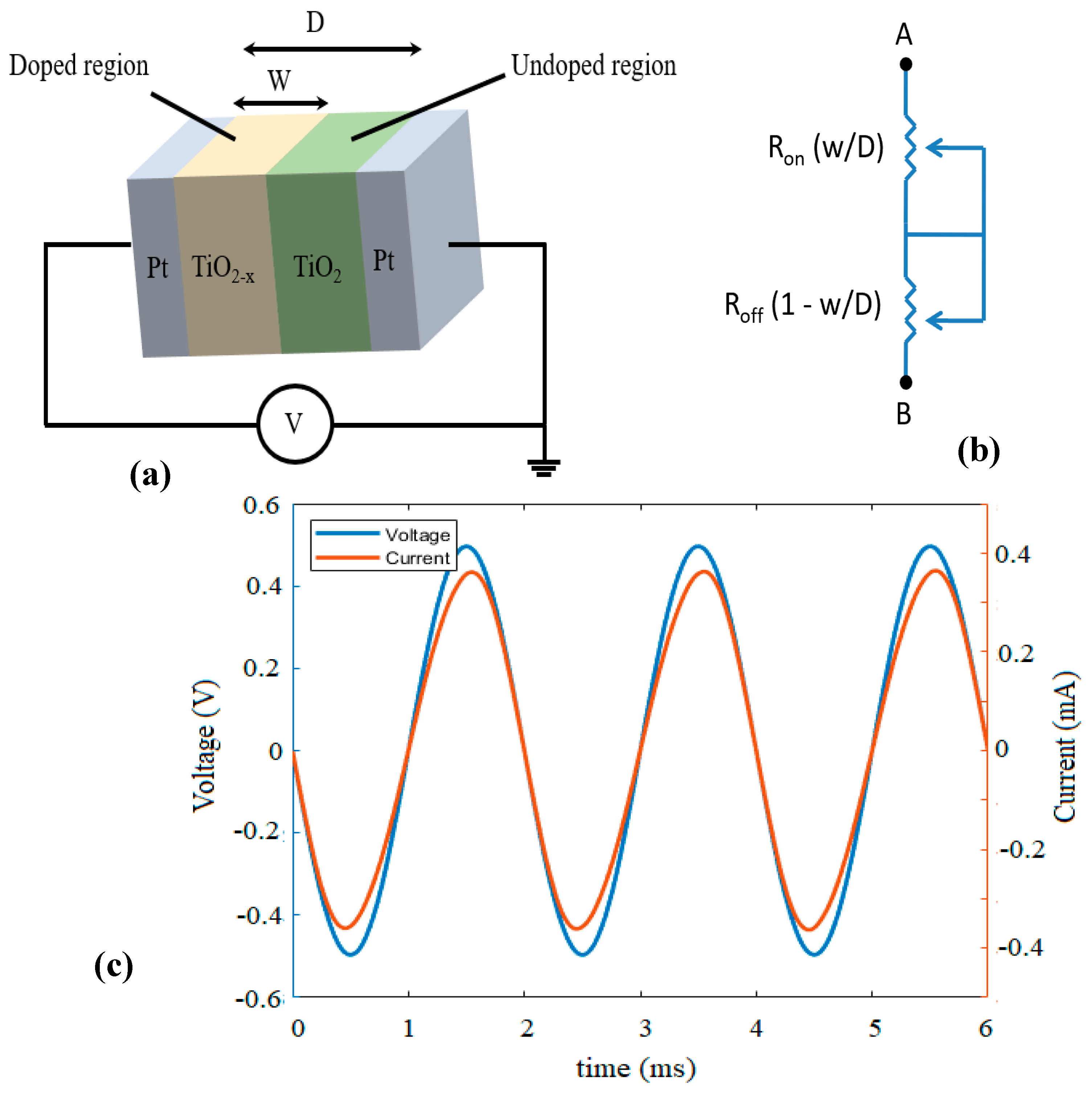
Figure 1(a) employed titanium oxide which is sandwiched between two platinum electrodes. Some part of dielectric TiO
2 is doped with charge carriers which lowers the resistance to R
on, while the other part is left undoped with high resistance R
off. By applying bias to a memristor, the boundary between doped (TiO
(2-x)) and undoped (TiO
2) regions move in either direction depending on the polarity of the applied voltage. This phenomenon can be modeled as two series-connected variable resistors as shown in
Figure 1(b). The state variable x is defined as the ratio of lengths of the doped region (w) to the undoped region (D), which represents the resistance states of the memristor, i.e., x=w/D. The I-V relation of a memristive device is dependent on the state variable and is given as [
25]:
where and are OFF- and ON state memristances.
One of the limitations of HP memristor is that the model does not include nonlinearities in ionic transport, especially in nanoscale devices. In 2009, Biolek developed nonlinear dopant drift memristor model using window function
(𝑥, 𝑖), which incorporates the boundary speeds and conditions [
29]. The first equation in (2) represents Biolek’s current (i) and voltage (v), second and third are state equations for Lehtonen-Laiho model.
In this work, the A13 memristor model is employed because of its high operating frequency, low complexity, high accuracy, and good switching properties. It is a modified version of both Lehtonen-Laiho [
30] and Biolek [
29] models. A13 has an activation threshold, so it can be used for high frequency impulse neural networks and non-volatile memory crossbars. Equation (2) summarizes both models:
If the applied voltage (
) is greater than the threshold (
), the rate of change of x with time is proportional to
. On the other hand, the memristor operates as a linear resistor for the
<
. The new window function of Biolek
and sigmoid function stpp(i) are related as [
31]:
By using parameter estimation, gradient decent algorithm to reduce mean square error, simulation annealing, the optimal values of the variables are:
;
; m = 0.000101;
Ω;
Ω;
V, p = 9.
Figure 1(c) shows memristor is a passive element because at every point v(t) = 0, current i(t) = 0.
In
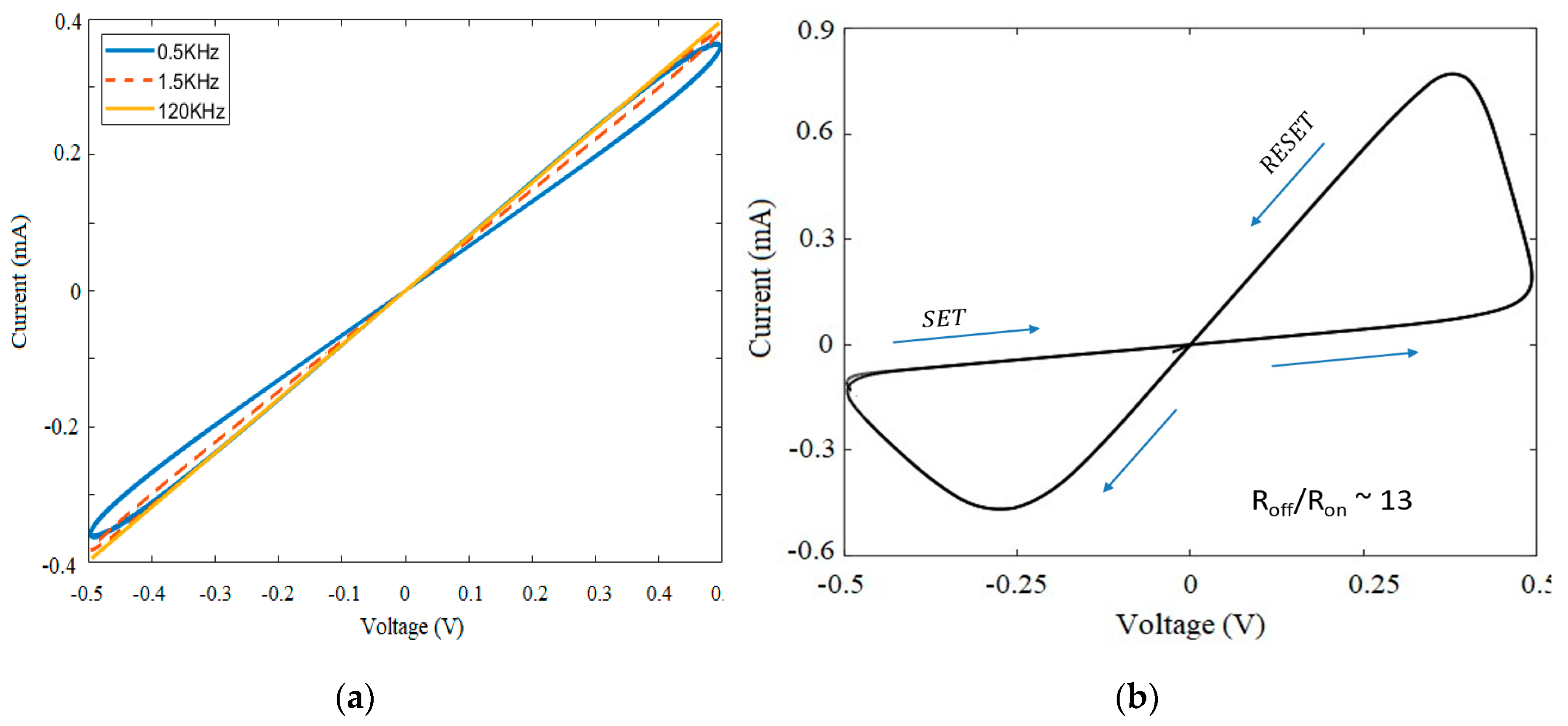
Figure 2(a), the memristor is simulated through different frequencies that are selected from the low frequency (0.5 - 1KHz), medium frequency (1KHz – 100KHz), and high frequency (> 100KHz) of a typical metal-oxide memristor. It is observed from the plot that the memristor reduces to a linear resistor at higher frequencies, which is a desirable feature in our proposed ternary logic.
The relationship between charge and flux of a memristor device is highly non-linear. Since A13 is mostly suitable for high frequency application, the hysteresis looks small even at low frequency. Sequel to this behavior, I-V curve in
Figure 2(b) is plotted at ultra-low frequency to clearly show pinched hysteresis loop for SET and RESET transitions. From the model’s optimal values for
and
,
and it represents the dynamic range of switching of the device. We can conclude that both the frequency of applied voltage and
are the main determinants of memristor characteristic loop.
3. 2D Field Effect Transistor
Due to its outstanding electrical, mechanical, and thermal properties, graphene, a sheet of carbon atoms that is two-dimensional (2D) and atomically thin, has drawn a lot of attention [
32]. Field-effect transistors (FETs) are a possible area of use for graphene, particularly graphene nanoribbon field-effect transistors (GNRFETs). This article gives a broad description of the process from basic graphene properties to GNRFET implementation and prospective applications. A special trinity of electrical, thermal, and mechanical characteristics distinguishes graphene from other materials. The ability to conduct electricity even at room temperature is demonstrated by its extremely high electron mobility, intrinsic bandwidth that is larger than that of many semiconductors, and other properties [
33]. Further supporting its suitability for electronics applications are its strong heat conductivity and mechanical strength. Graphene nanoribbons (GNRs) are confined graphene sheets that are gapless semiconductors, yet their electrical characteristics can be customized. GNRs can display metallic or semiconducting characteristics depending on their edge configuration (zigzag or armchair) [
34]. Importantly, it is possible to modify the bandgap of GNRs in order to create specialized electronic devices. The creation of GNRFETs is made possible by the bandgap modulation of GNRs. According to the GNRFET’s operating theory, a gate electrode receives an external voltage that controls the conductance of the GNR channel [
35]. Due to their scalable bandgap and excellent carrier mobility, GNRFETs have an advantage over conventional silicon-based FETs as the technology node gets smaller.
Researchers are looking into novel materials other than silicon because of the rising demand for smaller, quicker, and more efficient electronic gadgets. In the field of nanoelectronics, molybdenum disulfide (MoS2), a substance belonging to the transition metal dichalcogenides (TMDs) family, has become a popular material. To get from the basic properties of MoS2 to its use in field-effect transistors (FETs), this article gives a brief outline of the procedures involved. Each layer of the layered material MoS2 is composed of two planes of sulfur atoms sandwiching a plane of molybdenum atoms. MoS2 is a direct bandgap semiconductor when it is thick, but it changes into an indirect bandgap semiconductor when it is thinned to a single layer. This makes it an interesting material for use in electronics and optics. In monolayer MoS2, the shift from an indirect to a direct bandgap opens enticing possibilities. When compared to bulk silicon, the monolayer MoS2’s thin structure makes it easy to control the electric charge, which is very important for FETs. Additionally, due to its direct bandgap, low-power digital circuits can be realized and may be integrated into optoelectronic devices [
36,
37]. Its application in FETs is made possible by the isolation of monolayer MoS2, commonly accomplished through exfoliation or chemical vapor deposition (CVD) [
38]. In a MoS2 FET, the conductance of the channel, which is made of MoS2, is regulated by the gate voltage. These FETs have demonstrated high on/off current ratios, small subthreshold swings, and silicon-comparable carrier mobilities [
39]
A plane of tungsten atoms sandwiched between two planes of selenium atoms makes up each layer of the semiconductor WSe2. WSe2 displays an indirect bandgap in its bulk state, just like MoS2. However, it transforms into a direct bandgap semiconductor when reduced to a monolayer. For optoelectronic and electrical applications, this characteristic is extremely important. Monolayer WSe2 is useful for FETs due to its distinctive combination of electrical characteristics. Due to its two-dimensional structure and direct bandgap, it offers good gate control over the channel. Additionally, WSe2 is a desirable choice for p-type FETs since it offers better hole mobility than many other TMDs [
40,
41]. Exfoliation or chemical vapor deposition can be used to create WSe2 monolayers of superior quality [
42]. An external gate voltage controls how much current flow through a WSe2 channel in a WSe2 FET. These FETs offer excellent on/off current ratios, which makes them appropriate for use in digital applications. When compared to other TMD-based FETs, the performance of a properly engineered WSe2 FET, including subthreshold swings and carrier mobility, has been shown to be competitive [
43].
In this article, we employed an efficient HSPICE model of flexible TMDFETs with a refined ballistic enhancement factor (BEF). Although it contains different transistor models, MoS
2 and WSe
2 are chosen because several studies already showed their suitability for transistor. Similarly, MOS-GNRFET is favored over SB-GNRFET because of monotonic I-V characteristics, no voltage shifting and less affected by process variation. The number of nanoribbon (n
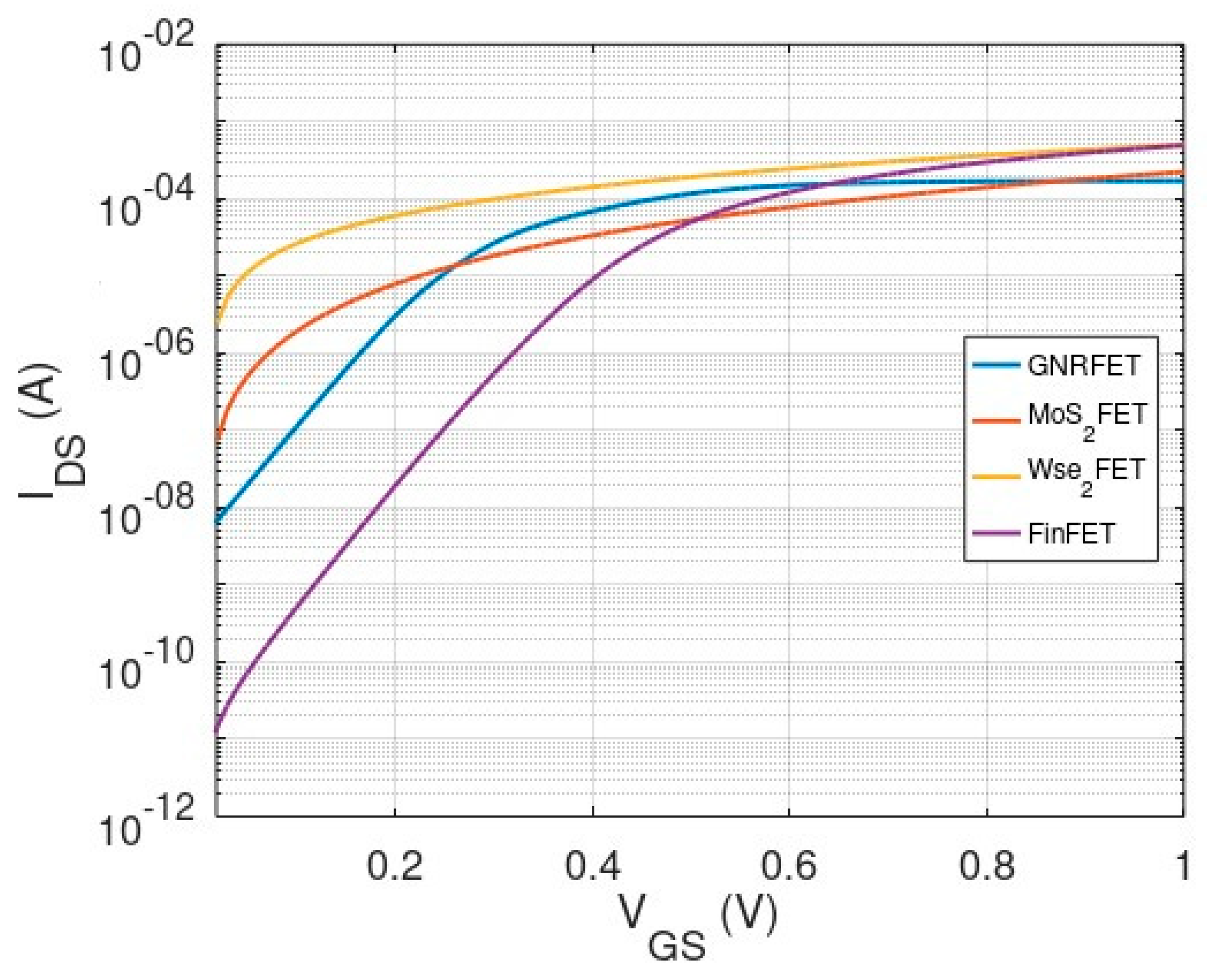
rib) and dimer lines (N), spacing between the ribbons, channel length, doping fraction, and oxide thickness of GNRFET model are scaled appropriately to ensure fairer comparisons with other TMDC transistors and FinFET. From the transistor I-V curve in
Figure 3, WSe
2 FET shows the highest
= 505 µA owing to its low effective mass and high carrier mobility. The inherent challenge of ambipolar transistor device is high
, so the unipolar multi-gate FinFET device has the best
= 14.5 pA.
4. Ternary Logic Gates and Characterization
There are basically two distinct logic levels in binary: False (0) and True (1). In ternary logic, a third logic level is added, and the discrete levels are False (0), Undefined (1) and True (2). The following basic operations can be implemented in ternary logic:
-
Inverter:
where is the ternary logic input variable, = [0, 1, 2]
TOR:
TNOR:
TAND:
-
TNAND:
where = [0, 1, 2]
In this proposed design, power supply is 1 V (
at logic ‘2′, 0.5 V
at logic ‘1′, and 0 V at logic ‘0′. When
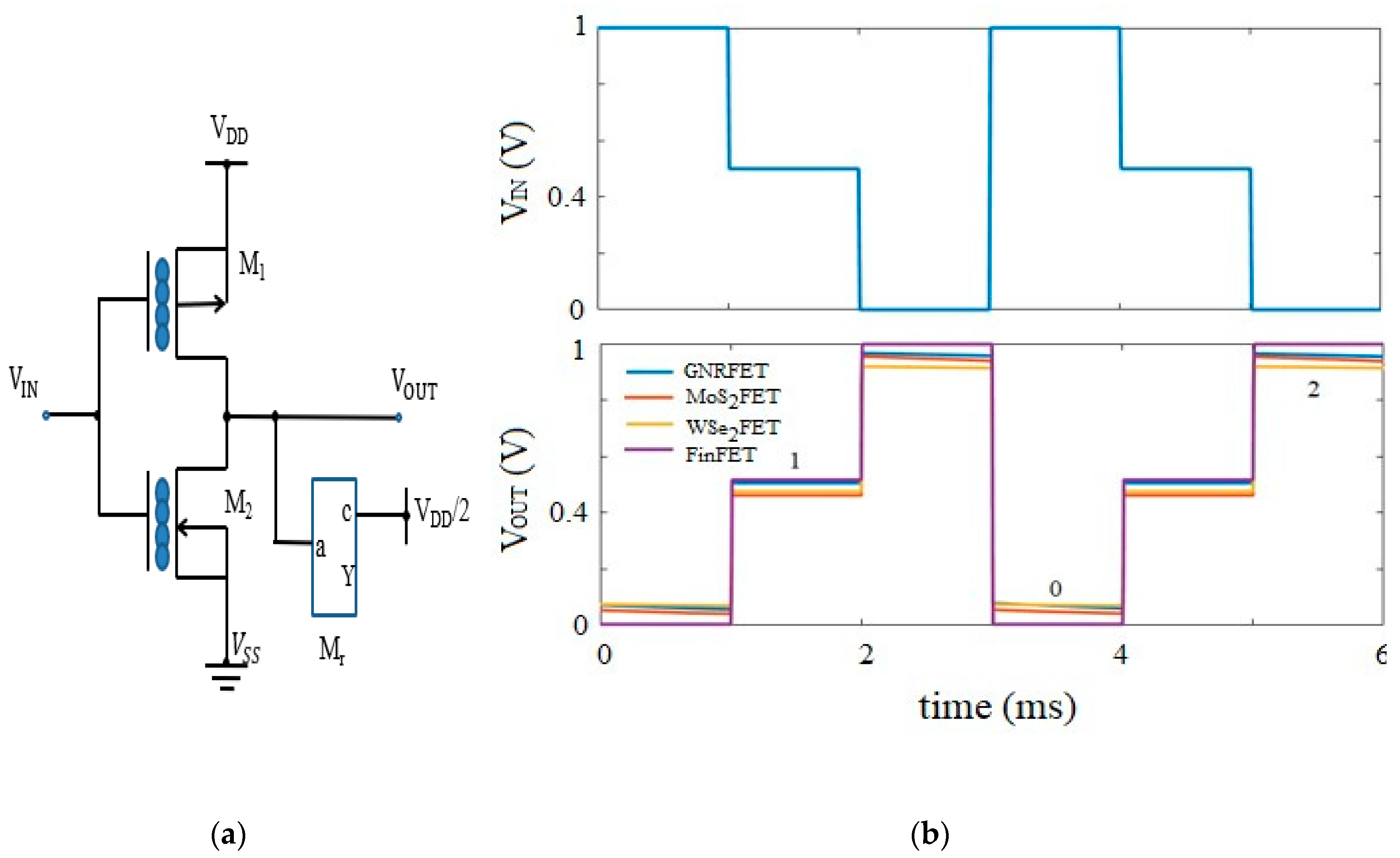
is at logic 0 for the inverter in
Figure 4(a),
is ON and
is OFF, which connects the output of inverter (
to
. Since current flows from high to low potential, the resistance of memristor
increases to
. Similarly, when
is at logic 2,
and
are OFF and ON, respectively, which connects
to 0 V. Invariably, the resistance of
decreases because of current flowing from terminal c to a.
Table 1 summarizes the truth table of ternary inverter logic.
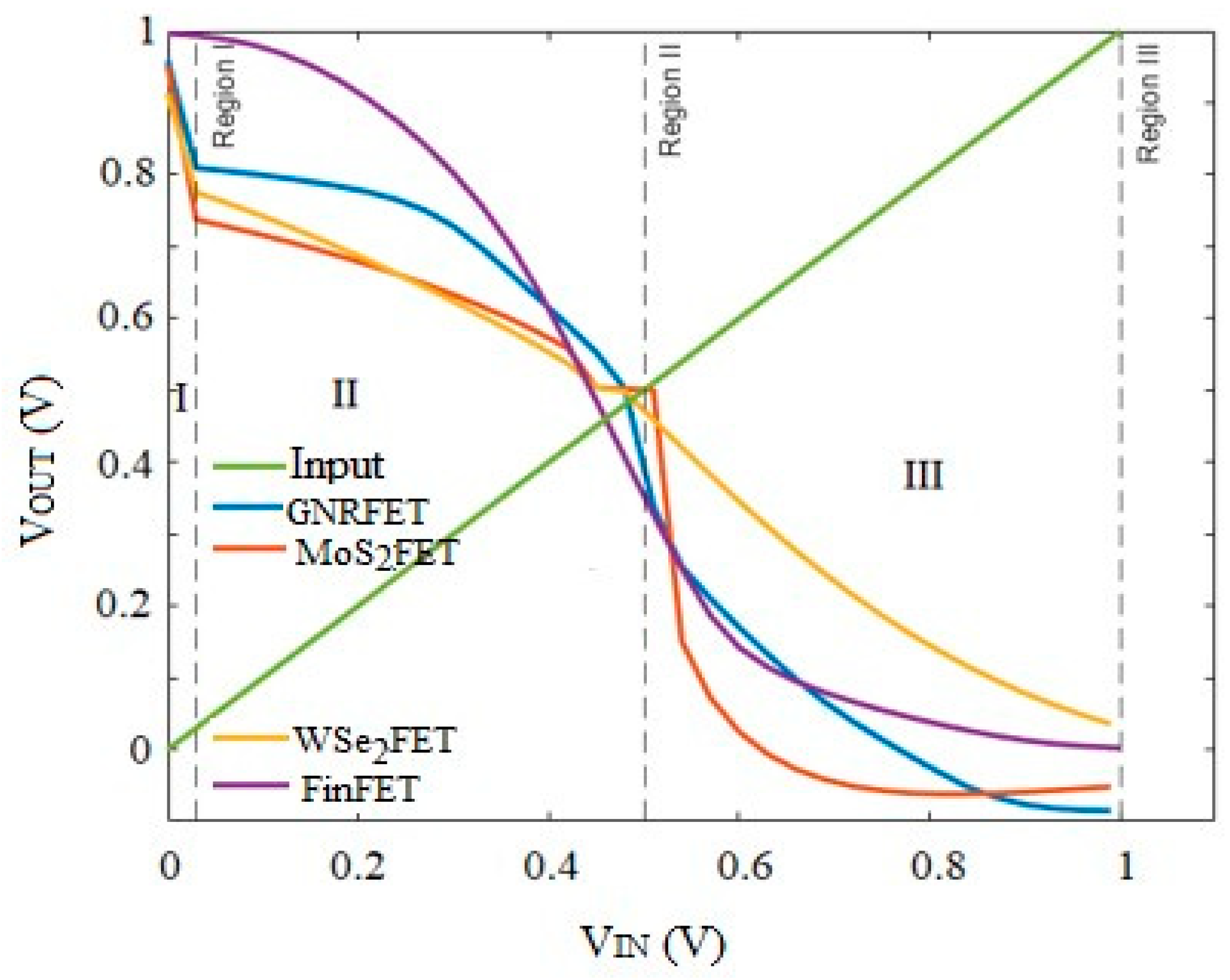
Figure 5 compares the voltage characteristic curves of various 2D materials-based and CMOS devices. The three states of some of the ternary logic in
Figure 5 are not clearly defined because of signal degradation caused by the memristor device. Nevertheless, the output voltage levels are discretized into three distinct states; any value that is greater than 0.7V is considered as logic 2, logic 1 corresponds to a voltage greater than 0.5V but less than 0.7V, and logic 0 is less than 0.5V. Signal restoration can be achieved by optimizing the size of n and p transistors, but there are trade-offs in power dissipation and die area.
The propagation delay, being an important performance metric, was estimated by averaging the delay of each transition in the entire simulation cycle. For each transition, delay was measured by taking 50% of both input and output of inverter. Similarly, the total energy consumed for each transition and energy delay product (EDP) is calculated as:
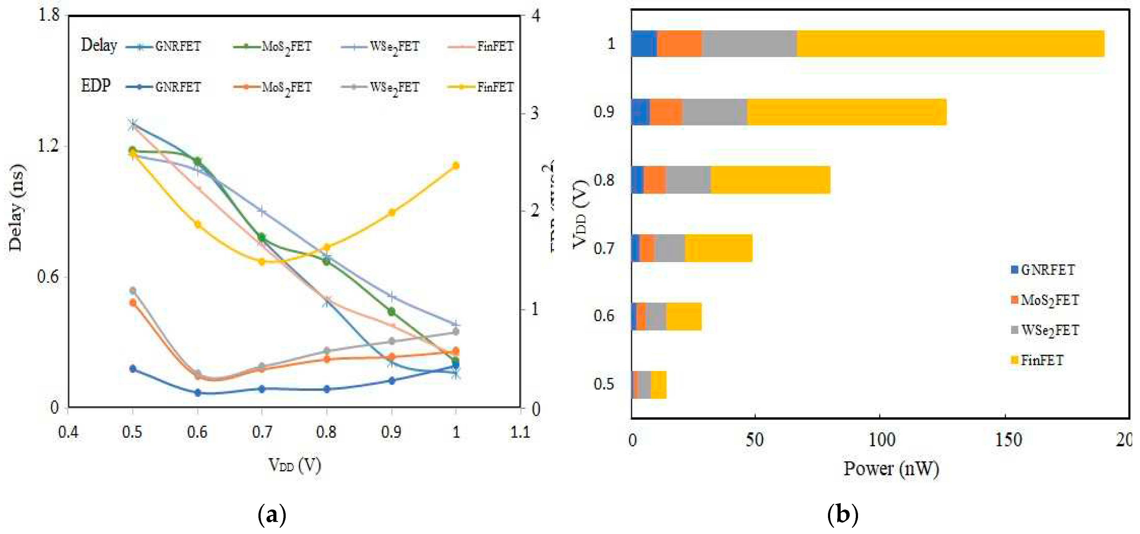
Figure 6 presents the variations delay, power, and energy with supply power for each transistor technology. The delay decreases with supply
for all technologies while energy delay product increases. A few crossings can be observed in the delay plots in
Figure 5(a), which means some of the inverters have the same value of delay at these intersections. For example, GNRFET and MoS
2 FET show a delay of 780 ps at 0.7 V supply. The steepy delay plots signifies a slight change in
causes a large change in propagation delay. MoS
2 FET shows the highest non-linearity in delay variations with supply power, and the worst-case delay at
= 0.5V is 1.3ns, 1.18ns, 1.16ns, and 1.29ns for GNRFET, MoS
2 FET, WSe
2 FET, and FinFET, respectively. Energy was estimated using
, where
is the average current when the output rises or falls, and
is the time difference. Subsequently, equation (5) was used to compute energy efficiency. From the rule of thumb that high speed circuits dissipate power and energy, EDP is used to critically examine the fundamental tradeoff between energy consumption and speed. All the inverters in
Figure 6 have their highest EDP at 0.5 V, and the energy efficiency of GNRFET decreases until 0.6 V where the optimum value is attained, after which EDP increases with supply power. Similarly, the optimum EDP for MoS
2 and WSe
2 FET are 0.33 fWs
2 and 0.35 fWs
2, respectively. At 0.7 V, FinFET achieves an optimum value of 1.49 fWs
2. By enhancing
from 0.6 to 0.7 V, the delay of each inverter decreases by 31.3%, 31%, 17.2%, and 26.5% while the energy consumption increases by 82.5%, 76.7%, 45.5%, and 8.5% for GNRFET, MoS
2 FET, WSe
2 FET, and FinFET, respectively.
The average power dissipated by each inverter is calculated by averaging the power consumption for all input transitions. It can be inferred from
Figure 6(b) that GNRFET logic dissipates the lowest power while the highest power consumption is recorded in FINFET. With respect to FinFET, the average power dissipation in GNRFET, MoS2 FET, and WSe2 FET inverter is reduced by a factor of 11.7X, 6.8X, and 3.2X, respectively.
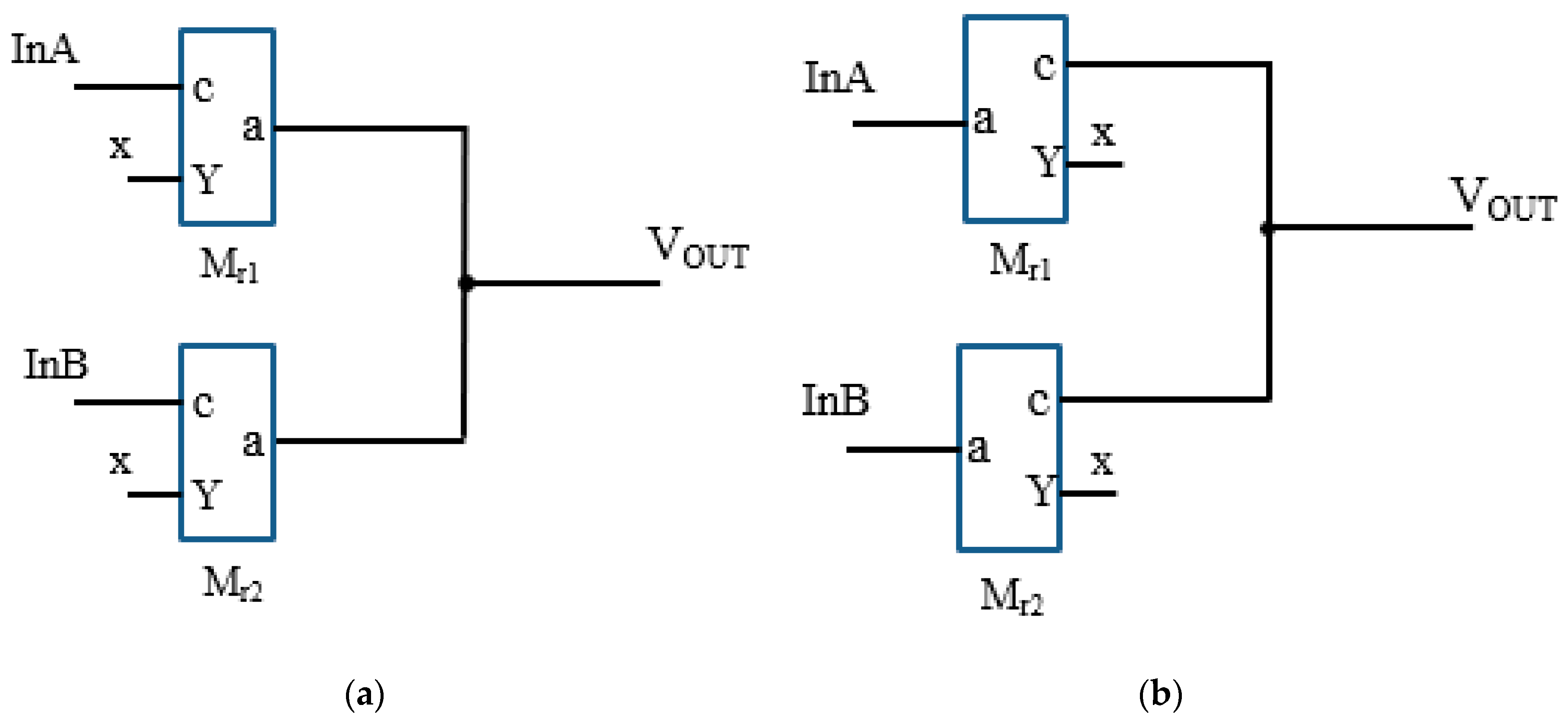
A two-input logic gate is discussed in this section. To understand the working principles of ternary logic gates, we will consider only the input vectors (2,0) (1,0) and (2,1). These combinations of input produce the same result as (0,2), (1,0) and (1,2). For OR gate in
Figure 7(a), when InA is at logic 2 and InB is at logic 0, current flows from terminal c of
to terminal c of
causing their resistances to increase (
) and decrease (
), respectively. By voltage divider, the output voltage of OR gate is given as:
logic 2 since
If the input vector is (1,0),
logic 1 since
As expected in a typical OR gate, the input vector (0,0) is the only combination that will produce an output = 0V (logic 0)
Considering vector (2,0) for a two-input AND logic in
Figure 7(b), current flows from terminal a of
to terminal a of
, thereby causing a decrease in the resistance of
and increase in
resistance. The output voltage is:
logic 0 since
If InA = 2 and InB = 1 or vice versa, the logic gate output voltage is obtained as:
logic 2 since
Ternary NOR (TNOR) and NAND (TNAND) logic gates can be instinctively constructed by connecting the outputs of TOR and TAND gates in
Figure 7(a,b) to a standard ternary inverter in
Figure 4(a). The logic operations of TNOR consists of two steps; it maximizes the two inputs InA and InB, and the intermediate result is inverted by a NOT gate to give the final output. If both inputs are at logic 0, the maximum value is “0” and the final output is
(logic 2). The output is
(logic 1) for a maximum input of “1”. If the maximum input is at logic 2, the output is 0V (logic 0).
For the TNAND, it also consists of two-step logic operations. It selects the minimum of the two inputs InA and InB and inverts the result. If the minimum input is at logic 0, TNAND produces output which is at logic 2. If the minimum input is at logic 1, the output is also at logic 1. If both inputs are at
(logic 2), the final output is “0”.
Table 2 presents the truth table of OR, AND, NOR and NAND ternary logic gates.
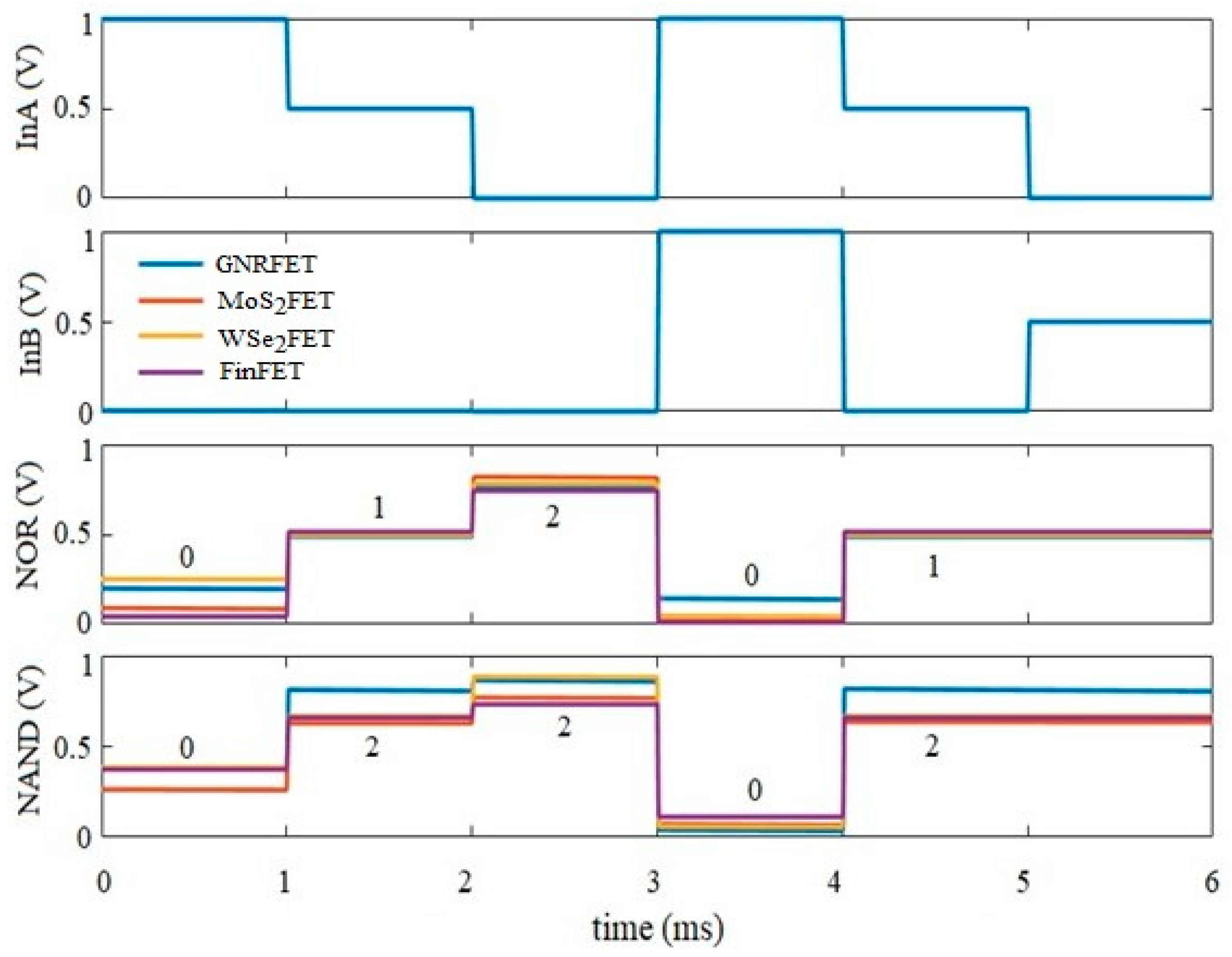
We have shown in
Figure 8 that memristor can operate in more than two logic states and it is a potential candidate to realize ternary logic. In addition, memristor is not only compatible with standard CMOS but also with other existing 2D technology processes. It is a small-sized device with nanoscale dimensions, so it can be stacked above GNRFET, MoS
2 FET, WSe
2 FET, and FinFET to save chip area. Unlike ref. [
44] that employed ten transistors to implement ternary NOR and NAND, our proposed design only uses three memristors and two transistors. Hence, there is a reduction of more than 50% in die area.
For future work and fabrication, each technology must be optimized to satisfy the requirements of low power cascaded logic gates. This can be achieved through proper engineering of device structure and contacts. A low work function metal can be employed as contact to improve the transistor behavior, and the use of a thin hBN and high-k 2D insulator can aid the control over Schottky barrier [
45].
