1. Introduction
At the 2022 United Nations Climate Change Conference, governments were called upon to review and enhance their emissions reduction targets for 2030 in their national climate strategies, while also advocating for an acceleration in the reduction of coal-derived energy use [
1]. Governments highlighted the importance of integrating low-emission energy sources and renewable energies to expand the diversity of energy sources and systems. The final agreement underscored the urgent need to invest in renewable energies, including technology and infrastructure, until 2030, with the aim of achieving net-zero greenhouse gas emissions by the year 2050 [
2].
Based on the aforementioned, there is a notable interest in advancing technologies related to solar cells, with the goal of increasing efficiency in the conversion of light energy into electrical energy. Therefore, the creation of tools that streamline the research of these devices emerges as an area of significant importance in the current context.
Within the realm of modeling solar cells and panels, series resistance typically symbolizes losses associated with metal contacts [
3]. Its identification is crucial in the modeling process. Typically, this resistance is determined by the slope of the I-V curve in the Voc (open-circuit voltage) region, characterized by low currents and high voltages [
4,
5].
However, it is crucial to note that the movement of electrons, which is responsible for the electric current, is influenced by the various junctions present in a solar cell, including those of metal-semiconductor and semiconductor-semiconductor [
6,
7].
In this work, a detailed analysis focused on the identification of series resistance (Rs) is presented. This analysis is applied to four solar cell fabrication processes developed at the National Institute of Astrophysics, Optics, and Electronics (INAOE), each with an area of 1 cm² [
8]. As a result of this study, four I-V curves are obtained, each corresponding to one of these procedures.
This analysis ranges from calculating the series resistance based on semiconductor physics parameters to determining Rs by applying the straight-line slope technique to the I-V curve of each manufactured device.
2. Series resistance (Rs) components and c-Si structure
The most prominent parameter of solar devices is efficiency, as it to some extent determines the quality of the solar cell and its technology. To achieve a high-quality solar cell, it is necessary to minimize potential losses.
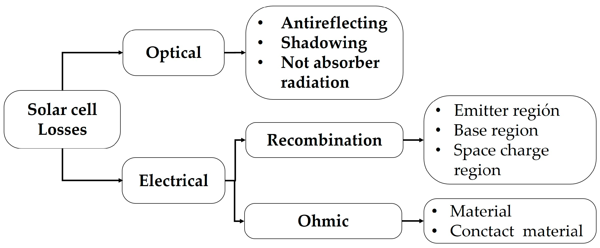
Figure 1 presents a diagram illustrating some of the possible losses in solar cells, which can be classified into two general groups: optical and electrical.
The electrical losses shown in
Figure 1 can be of two types: recombination losses and ohmic losses. In this study, we will focus solely on investigating the latter, specifically losses associated with the material and metal contacts [
3].
2.1. Influence on the efficiency of ohmic resistances
Solar cells often exhibit parasitic resistances both in series and shunt. These resistances have a significant and disadvantageous impact on the performance of solar cells as they dissipate energy in the form of heat. In most cases, and for typical values of parallel and series resistances, the primary consequence of parasitic resistance is the reduction of the fill factor and, consequently, the efficiency of the solar cell [
10].
Several physical mechanisms are responsible for the presence of these resistances. The major contribution to series resistance (Rs) comes from the resistance of the semiconductor material constituting the cell, as well as the resistance of the semiconductor material in contact with the metal contacts. On the other hand, shunt resistance (Rsh), originates from leakage across the p-n junction around the edge of the cell and in non-peripheral regions, especially in the presence of crystal defects and precipitates of foreign impurities in the junction region [
9].
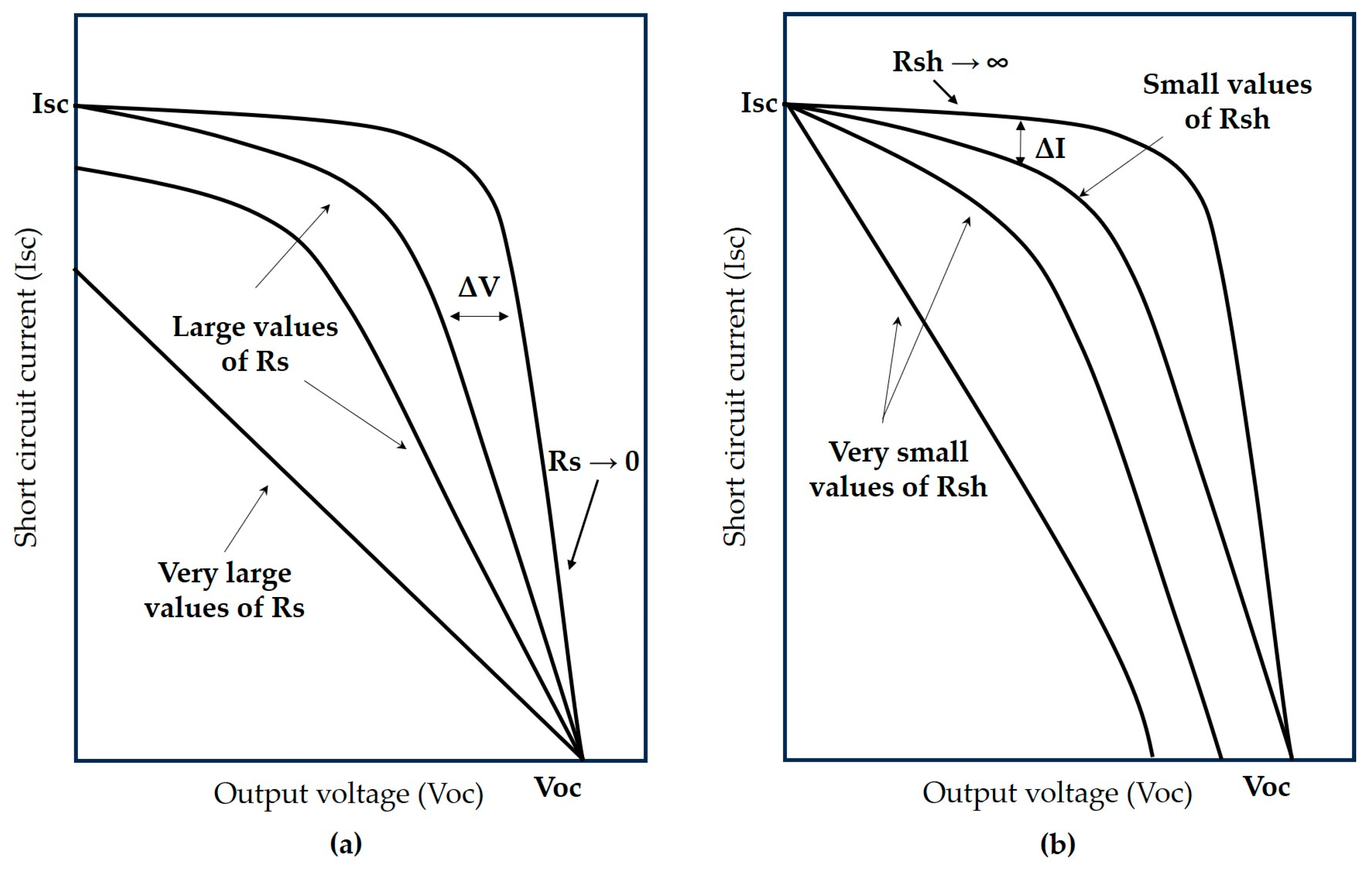
Shunt and series resistances are generally calculated from the slope of the I-V characteristic curve [
11]. In
Figure 2, the effects of each of these resistances on the shape of the curve can be observed.
In
Figure 2(a), the impacts on the I-V curve are shown when high values of Rs are present, as ideally, this resistance should tend towards zero.
On the other hand, in
Figure 2(b), having small values of shunt resistance also results in deformation of the I-V curve, as ideally, this resistance should be as large as possible, tending towards infinity [
3].
2.2. Components of the series resistance (Rs)
The series resistance, commonly represented as Rs, generally arises from both the inherent resistance of the semiconductor material forming the solar cell and the resistance of the semiconductor material at the interface with the metal contacts [
10].
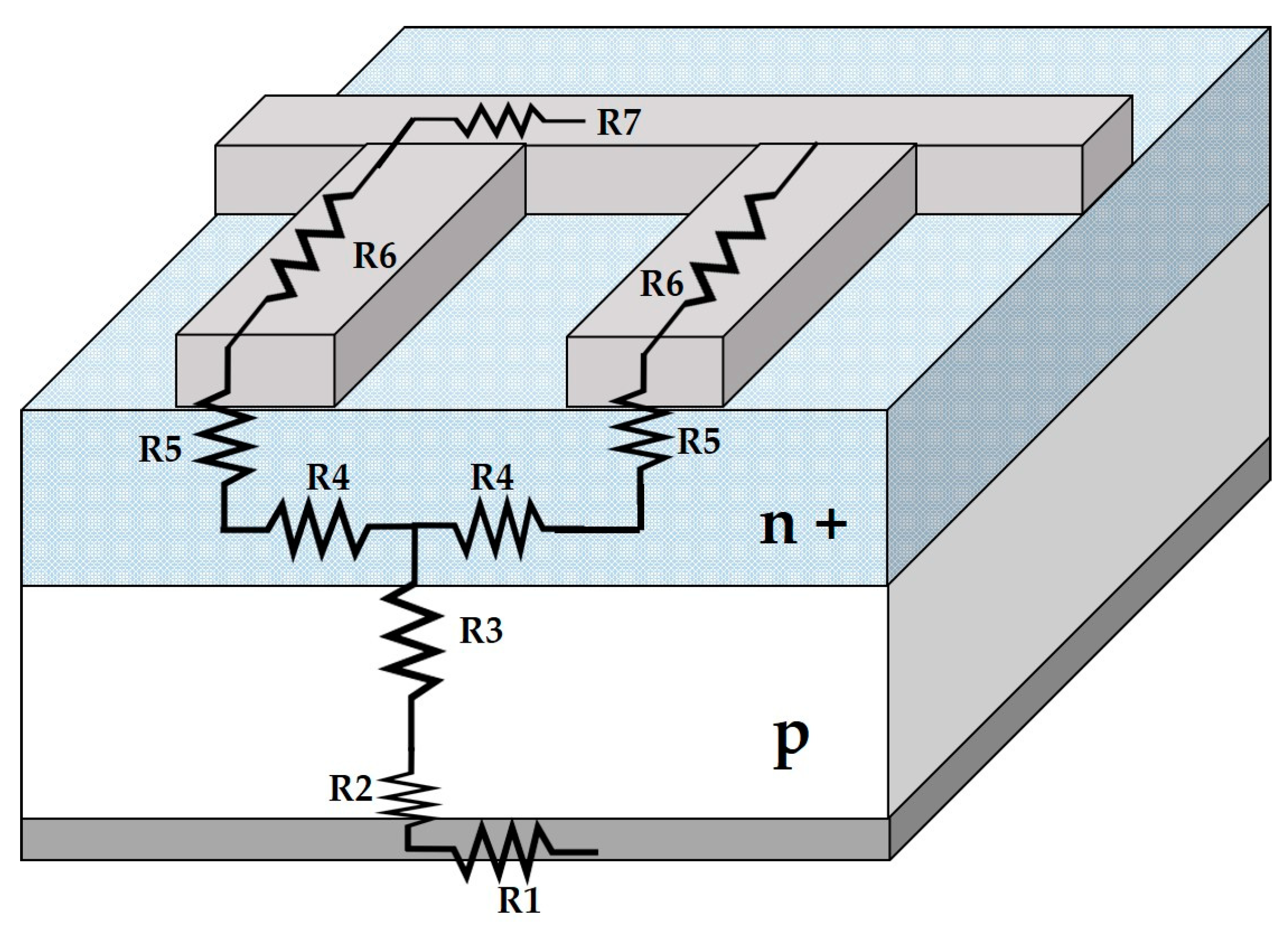
Figure 3 better illustrates each of the components of series resistance.
Each of the resistances presented in
Figure 1 represents the following [
3]:
| R1 |
Back metal contact |
| R2 |
Metal-semiconductor contact across the entire back surface |
| R3 |
Semiconductor material (base) |
| R4 |
Resistance of the emitter between two grid fingers |
| R5 |
The metal-semiconductor contact of the grid finger |
| R6 |
Grid finger resistance |
| R7 |
Busbar resistance |
To calculate each of the components of Rs, the equations presented in
Table 1 can be used.
The detailed explanation of each component that integrates the equations provided in
Table 1 is available in
Table 2.
To calculate
and
, it is essential to take into consideration the height of the potential barrier generated by the contact between the metal and the semiconductor, considering whether it is of n-type or p-type, for the n-type case, we have [
3]
for the p-type contact, we have:
Where
|
Height of the metal-semiconductor barrier. |
|
Work function of the metal |
|
Work function of the semiconductor |
|
Bandgap of the semiconductor |
Once the barrier height has been calculated, it is possible to determine the specific contact resistivity. This resistivity is influenced by how electrons move between the metal and the semiconductor. This movement can occur through either the tunneling effect or the thermionic effect, depending on the doping level of the semiconductor.
So, for the tunneling effect, it is given by
Where
A*= Richardson constant (1.2 x 10⁶ A/m2K2)
m* = rest mass of the electron
While, for the thermionic effect, it can be calculated as:
Where
k = Boltzmann constant
q = charge of the electron
T = Temperature
2.3. Single-junction c-Si solar cells
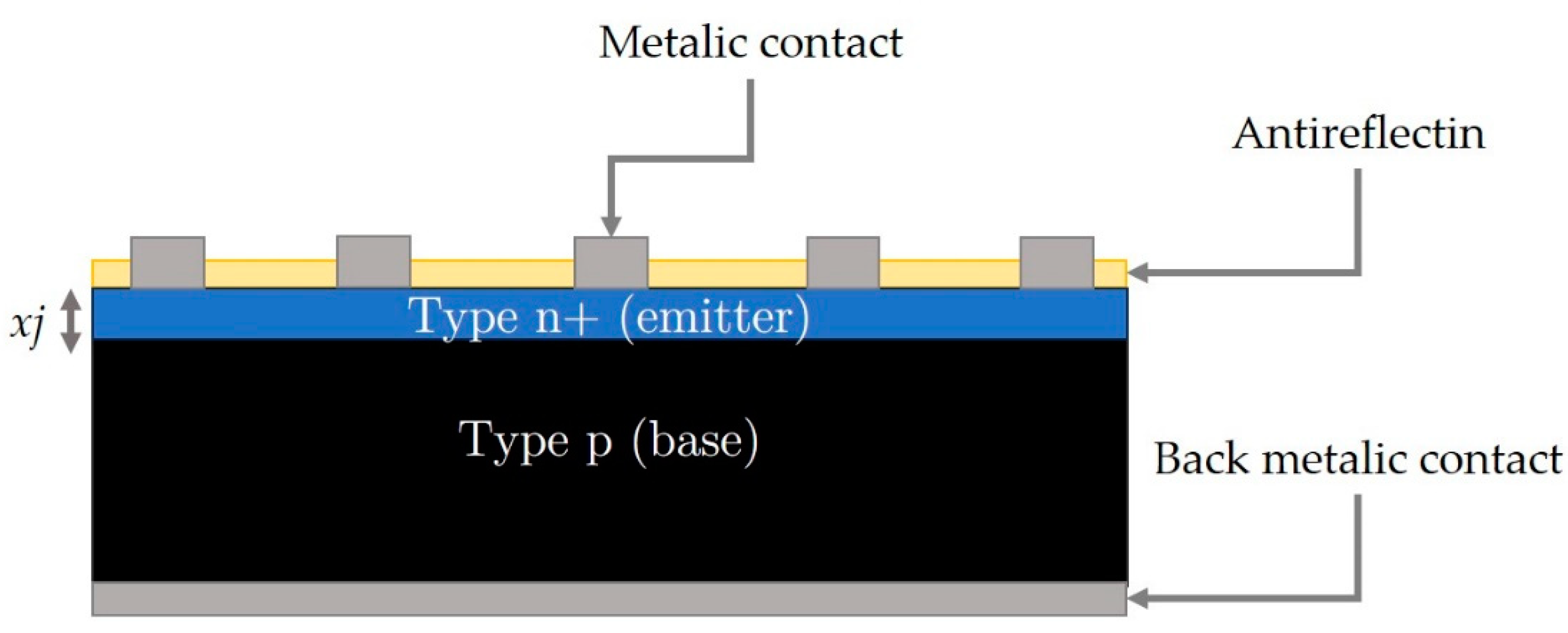
In [
8], the manufacturing process of solar cells with a simple structure based on c-Si is detailed.
Figure 4 provides a comprehensive illustration of the configuration of these cells.
As shown in
Figure 4 solar cells with a simple structure are basically composed of a p-n+ junction, without texturing, an anti-reflective layer usually made of SiO
2, and the upper and lower metal contacts [
8].
A crucial parameter in these cells is the junction depth (
xj). Therefore, optimizing this factor contributes to achieving improved efficiencies since the latter will be directly affected by the series resistance (Rs) [
8].
In [
8], four manufacturing processes (I-IV), were carried out with the aim of finding the optimal junction depth that would result in the best efficiency, as detailed in
Table 3.
As observed in
Table 3, the variation in junction depth has a direct impact on the efficiency of the solar cell. Changing from 0.87 to 0.60 results in a 2.4% increase in efficiency.
2.3.1. Influence of sheet resistance on the efficiency of the solar cell
The sheet resistance, R
SH, indirectly affects the efficiency of the solar device, depending on the magnitude it can reach, whether it is a uniformly doped substrate or a non-uniformly doped one [
13].
For uniformly doped substrates, R
SH can be determined according to:
Where:
t = thickness of the substrate
= resistivity of the material
σ = conductivity of the material
While for non-uniformly doped substrates [
9,
13], R
SH can be calculated as:
Where
q = charge of the electron
xj = junction depth of the emitter
μn = electron mobility
C(x) = concentration profile
On the other hand, sheet resistance can also be calculated experimentally using the four-point technique, this technique as described in reference [
13] with more details.
As described in previous sections, a solar cell is the junction of two materials, p-n, with the substrate generally being of p-type. For the emitter, diffusion or ion implantation processes are typically carried out [
9], which, according to equations (5) and (6), will modify the R
SH of the substrate based on the junction depth between the materials. This implies that R
S will also undergo changes according to these parameters, and in turn, it will modify the final cell efficiency as shown in
Table 3.
2.4. Top contact grid
A fundamental aspect that significantly influences series resistance (R
S) is the nature of the metallic contacts, as they are responsible for facilitating the flow of electrons from the cell to the load [
14].
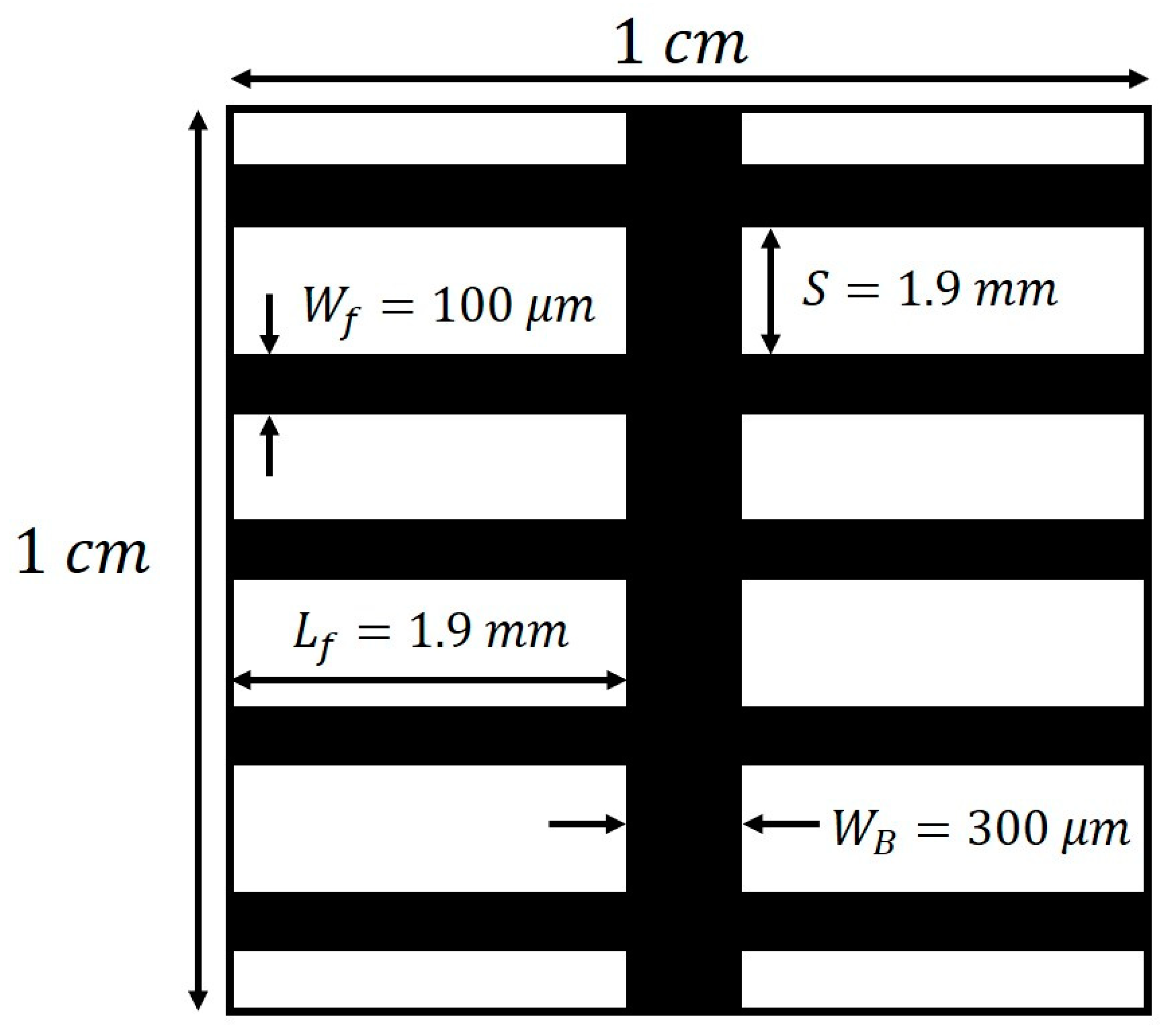
Figure 5 illustrates the configuration of the front grid, which commonly consists of a main bus and transverse collector bars, known as “fingers” [
15].
In
Figure 5, the geometry of the contact grid used for the simple-structured cells described in [
15] is depicted. For the upper contact, typically, the metal deposition covers the entire surface. In specific cases, contact windows are opened, which help enhance the efficiency of the device.
2.5. Configuration of resistances for the calculation of Rs
In the previous section, the components constituting the series resistance (R1-R7), as well as the structural characteristics of the p-n junction and the geometry of the top contact grid, were described.
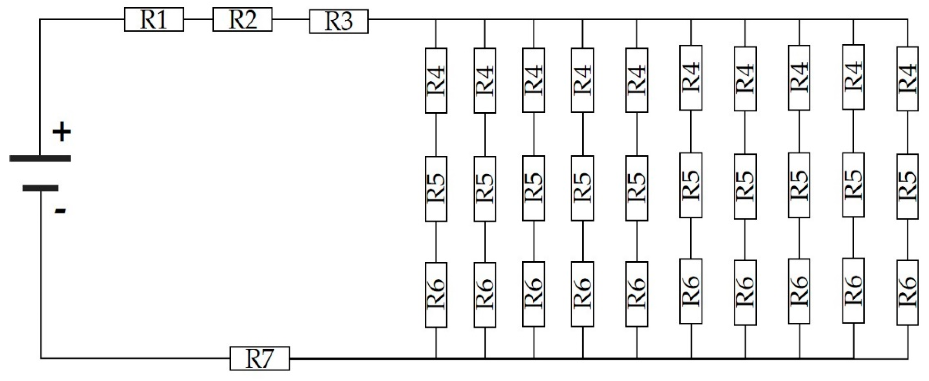
To perform the analysis and calculation of series resistance, a resistor network is proposed as shown in
Figure 6. This circuit takes into account the contact resistance (metal-semiconductor) generated in each finger of the top grid (R4), the current between each grid finger (R3), and the resistance of the grid finger (R5). Since each finger is connected to the busbar, it is considered that each resistance generated by R3-R5 is in parallel with the next finger.
In the previous figure, resistors R1, R2, R3, and R7 represent common resistances associated with the rear metal contact, which is shared anywhere in the cell, as well as the contact with the p-type semiconductor, substrate resistance, and busbar.
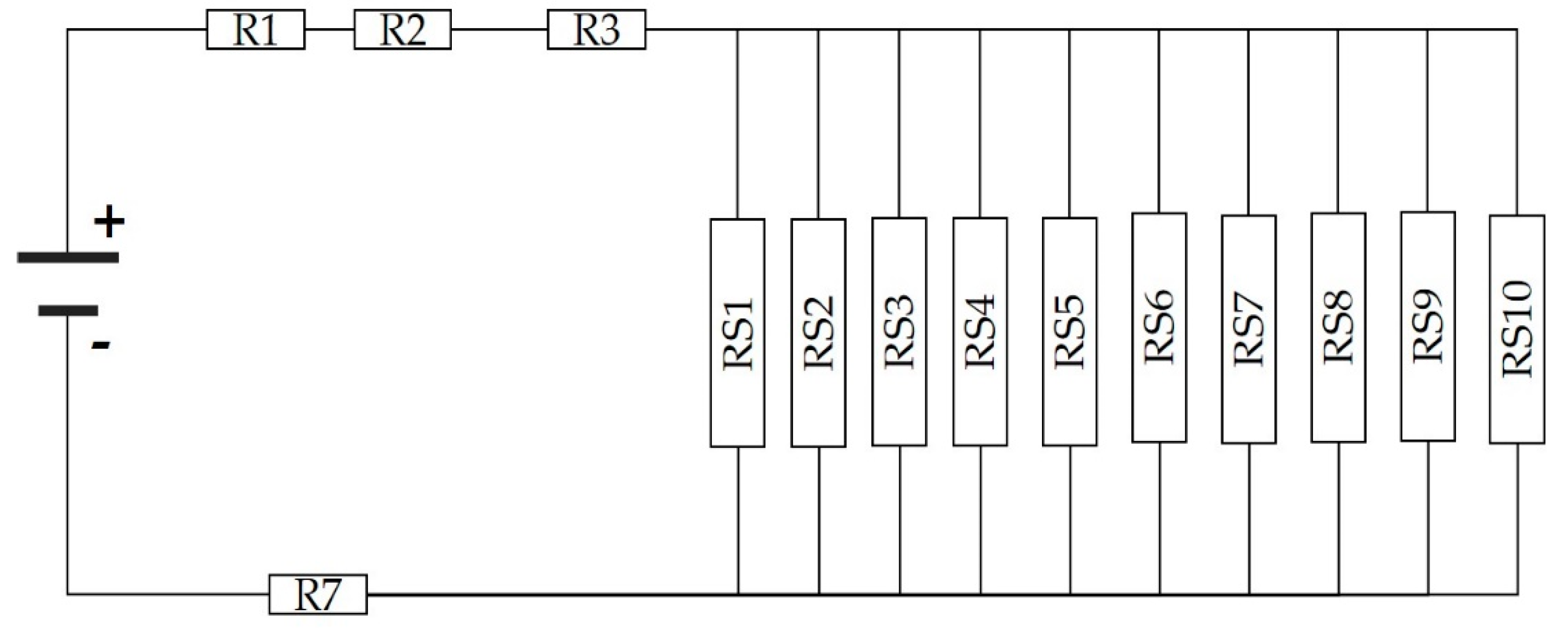
The resistance associated with each finger will be determined by the next equation
The equation (5) will provide a series resistance for each finger, resulting in
,
,
, ...,
. With this series resistance, the configuration of the resistor network presented in
Figure 6 will be simplified as shown in
Figure 7.
With the new resistor configuration shown in
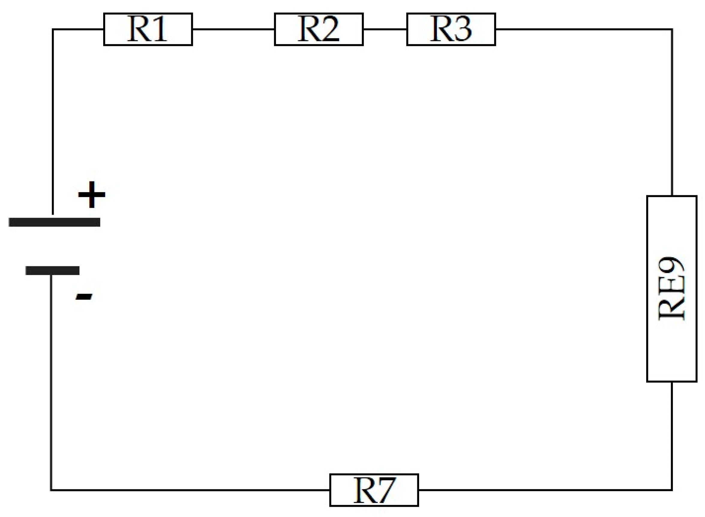
Figure 7, the circuit analysis is once again performed, calculating the parallel resistance (6) until obtaining the equivalent resistance
. This will enable the final calculation to determine the value of Rs.
The resulting equivalent resistance is shown in the new resistor configuration in
Figure 8. Through this updated arrangement and by once again conducting the circuit analysis (7), the value of the series resistance (Rs) of the cell is determined.
With equation (9), it is possible to calculate the total series resistance, considering all its components, from the substrate to the metal contacts.
3. Results
In this section, the calculations are presented using the equations from
Table 1 to estimate R1-R7, along with equations (1)-(5) and (7)-(9).
Table 4 details the parameters related to both the grid geometry and the properties of the materials (the substrate and conductive material).
Since they have different properties, p-type material and n-type material, the sheet resistance is determined according to equation (6), taking a resistivity of 5 Ω-cm, in the case of the substrate (RSHSUB), and using the four-point technique in the case of the emitter (RSHE).
The variations of R
SHE and R
SHSUB, depending on the junction depth of each manufacturing process I-IV, are detailed in
Table 5.
Table 5 shows how R
SHE and R
SHSUB vary when adjusting
xj. By applying equation (6) with a resistivity of 5 Ω-cm for the substrate, the thickness t
sub will be modified based on the junction depth, and consequently, R
SHSUB will change.
Obtaining R
SHSUB using the four-point technique allows determining the resistivity of the substrate (p-type), even without forming the pn junction.
Table 6 presents a comparison between parameters obtained experimentally and the calculus obtained theoretically by applying equation (6).
Table 6 shows the comparison between experimentally obtained R
SHSUB and theoretically calculated R
SHSUB. For these calculations, a value of ρ
SUB of 8.5 Ω-cm was used, generating a discrepancy in R
SHSUB of less than 3%. Nevertheless, it is evident that the application of equation (6) is effective for calculating R
SH in situations where the substrate is uniformly doped.
Using the experimental resistivity, calculations for the components of the series resistance (R1-R7) are carried out, considering both R
SH for each side of the cell and R
SHSUB and R
SHE for the substrate and emitter, respectively. These calculations take into account that these components are affected by the junction depth in each process.
Table 7 presents the results obtained for each of these components.
Table 7 displays the results derived from the application of the equations detailed in
Table 1. It is observed that R
SHSUB and R
SHE vary with the junction depth, directly impacting the components dependent on these parameters.
R3 is not directly linked to RSHSUB but depends on the thickness of the p-region (tPR), whose value is modified according to the depth of the emitter, ranging between 0.87 µm and 0.60 µm.
R1, R6, and R7, depending on the grid geometry and conductor thickness, remain unchanged with changes in R
SH. Their resistance stays constant and is only presented in the first section of
Table 7 for a depth of 0.87 µm.
R4, R5, and R6 are simplified into Rs1-10 using equation (7), and by applying equation (8), RE1-9 is obtained.
Table 8 details the values of each RE9 for various junction depths, with this resistance being crucial for calculating the total series resistance (Rs) of the cell through equation (9).
Table 8 shows how the series resistance varies with junction depth, confirming that a decrease in xj results in a reduction in series resistance, demonstrating the influence of RSH on total Rs.
The results obtained in the series resistance calculation, presented in
Table 8, are complemented by the series resistance obtained through a parameter extraction model [
16]. This model involves calculating the slope of the solar device’s I-V curve in the Voc branch, where series resistance has a greater impact.
Table 8 also shows the percentage difference between the calculations and the parameter extraction method.
Table 8 indicates that, in each case of efficiency improvement, the series resistance tends to decrease, in line with the theory outlined in
Section 2.1 of this work. Although the differences between theoretical Rs and that obtained by parameter extraction may seem “high,” this could be due to the conditions under which the cells were obtained or characterized for the I-V curve. Nevertheless, it is demonstrated that the Rs calculation follows a similar behavior to the parameter extraction model.
4. Discussion
In the study conducted by [
17], the optimization of the top contact grid is addressed with a limited focus, as it solely concentrates on that part and generalizes a system of equations based on the number of buses that the top contact can contain. However, it does not delve into other elements of series resistance. While it presents a proposal for an arrangement of resistances that considers all its components in series, this approach only works within the scope of that study by not analyzing the substrate’s characteristics and by considering only the upper metallic contact.
In [
18], c-Si cells are examined with an emphasis on optimizing the fingers that make up the grid to minimize losses caused by partial or total shading. Although the components of series resistance are generally mentioned, the study focuses solely on increasing the width or height of two of the grid fingers through aluminum and silver deposits as metallic contacts.
In the study by [
19], the investigation focuses on PERL and LGBC-type cells, addressing the components of series resistance. However, the analysis specifically centers on the metal-semiconductor contact in the front grid and the contact windows on the rear. It discusses how the implementation of high doping and the use of a low-resistivity conductor, such as silver, contribute to improving the efficiency of the solar cell in these regions. Despite these observations, there is no explicit presentation of an equivalent circuit that models the losses associated with series resistance. Overall, the research is concentrated on analyzing metallization techniques to achieve optimal metal-semiconductor contact.
In the article [
20], an equivalent circuit is introduced to model losses associated with series resistances, accompanied by a set of equations to calculate these resistances. However, the research focus once again centers on the upper grid. While a comparison between experimental and theoretical results is mentioned, the article lacks information regarding the specific technology of the studied solar cells. Additionally, a direct comparative table of the obtained results is not provided, limiting the assessment and understanding of the effectiveness of the proposed model.
Contrary to these cases, the present work demonstrates that, for a simple-structured cell, factors other than metallic contacts influence Rs, such as junction depth, which alters the properties of p-n materials, modifying the RSH, which is also part of the final Rs. Additionally, a circuit is proposed that models the components of Rs, considering it as a series resistance, without assuming that all its components are in series as well.
5. Conclusions
The current study establishes that series resistance (Rs) is not exclusively confined to the front metal contacts (grid), as commonly asserted. It has been demonstrated that additional factors, such as junction depth (xj), influencing sheet resistance (RSH), are integral to manufacturing processes. The consideration of RSH is critical, as elevated values of this component lead to increased Rs values. In [
9], there is a proposal for the use of substrates with a thickness of 100 μm, as such substrates achieve heightened efficiencies.
The cells employed in this research exhibit a simple structure, lacking surface texturing or rear contact windows, providing a baseline for future analyses of more intricate cells. Furthermore, a resistance arrangement is introduced to model the distinct components of series resistance. While this model serves as an initial approximation, displaying acceptable and theory-consistent outcomes, it can be refined in subsequent studies to better accommodate more complex cell structures.
In summary, this study contributes to the understanding of various parameters constituting series resistance, impacting solar cell efficiency by modifying any of these factors. The broad assumption that only metal contacts are responsible for losses associated with Rs in solar cells is deliberately avoided.
Authors are encouraged to delve into a discussion of the results, exploring their interpretations in the context of prior studies and working hypotheses. The implications of the findings should be thoroughly examined within the widest possible context. Additionally, authors have the opportunity to spotlight potential future research directions.
References
- World Meteorological Organization, “Climate and Weather Extremes in 2022 Show Need for More Action”, , 2022. https://public.wmo.int/en/media/news/climate-and-weather-extremes-2022-show-need-more-action. 23 December.
- United Nations Environment Programme (UNEP), “COP27 Ends with Announcement of Historic Loss and Damage Fund”, , 2022. https://www.unep.org/news-and-stories/story/cop27-ends-announcement-historic-loss-and-damage-fund. 22 November.
- Goetzberger, Adolf, Joachim Knobloch, and Bernhard Voss. Crystalline silicon solar cells. John Wiley & Sons Ltd 1,1998.
- Venkateswari, Radhakrishnan & Rajasekar, Natarajan. (2021). Review on parameter estimation techniques of solar photovoltaic systems. International Transactions on Electrical Energy Systems. 31. [CrossRef]
- Raafat, Samuel & Hasanien, Hany & Turky, Rania & Abdel Aleem, Shady & Calasan, Martin. (2022). A Comprehensive Review of Photovoltaic Modules Models and Algorithms Used in Parameter Extraction. Energies. 15. 8941. [CrossRef]
- McEvoy, A. , Markvart, T., Casta~ner, L., Markvart, T., & Castaner, L. Practical handbook of photovoltaics: fundamentals and applications. Elsevier, 2003.
- SM Sze and KK, Ng. Physics of semiconductor devices John wiley sons, 2006.
- José de Jesús Martínez Basilio, Mario Moreno Moreno, Pedro Rosales Quintero, Desarrollo e Investigación de un Proceso de Fabricación de Celdas Solares Basadas en la Tecnología del c-Si, INAOE, Tesis de Doctorado, (2017).
- Green, M.A. (1981). Solar Cells: Operating Principles, Technology and System Applications.
- Saikrishna, G. , Parida, S. K., & Behera, R. K. (2015). Effect of parasitic resistance in solar photovoltaic panel under partial shaded condition. 2015 International Conference on Energy Systems and Applications. [CrossRef]
- Van Dyk, E. E. , Meyer, E.L. Analysis of the effect of parasitic resistances on the performance of
photovoltaic modules. Renewable Energy 2004(29), 333–344. [CrossRef]
- Eitel Leopoldo Peltzer y Blanca; INTRODUCCIÓN A LA FÍSICA DE SEMICONDUCTORES Y DISPOSITIVOS ELECTRÓNICOS; Universidad Nacional de la Plata; edulp, Buenos airea argentina, primera edición, 2021.
- Dieter K Schroder. Semiconductor material and device characterization. JohnWiley & Sons, 2006.
- Gupta, D. K. Langelaar, M., Barink, M., van Keulen, F. Topology optimization of front
metallization patterns for solar cells. Structural and Multidisciplinary Optimization 2014, 51, 941–955. [Google Scholar] [CrossRef]
- Oscar J Velandia Caballero, Mario Moreno Moreno, Pedro Rosales Quintero, Estudio y desarrollo de celdas solares basadas en estructuras de silicio cristalino / silicio amorfo dopado, INSTITUTO NACIONAL DE ASTROFÍSICA ÓPTICA Y ELECTRÓNICA, Tesis de maestría, Puebla, México, 2018.
- M. J. Heredia-Rios, L. M. J. Heredia-Rios, L. Hernandez-Matinez, M. Linares-Aranda and M. Moreno-Moreno, “Non-iterative parameter extraction method based on the single diode model (SDM).,” 2023 IEEE Latin American Electron Devices Conference (LAEDC), Puebla, Mexico, 2023, pp. 1-5. [CrossRef]
- Caballero, Luis Jaime. (2010). Contact Definition in Industrial Silicon Solar Cells. [CrossRef]
- Hong, Ji-Hwa & Kang, Min Gu & Kim, Nam-Soo & Song, Hee-Eun. (2012). Multi-layer Front Electrode Formation to Improve the Conversion Efficiency in Crystalline Silicon Solar Cell. Journal of the Korean Institute of Electrical and Electronic Material Engineers. 25. [CrossRef]
- Ebong, A. , & Chen, N. (2012). Metallization of crystalline silicon solar cells: A review. High Capacity Optical Networks and Emerging/Enabling Technologies. [CrossRef]
- Handy, R. J. (1967). Theoretical analysis of the series resistance of a solar cell. Solid-State Electronics, 10(8), 765–775. [CrossRef]
|
Disclaimer/Publisher’s Note: The statements, opinions and data contained in all publications are solely those of the individual author(s) and contributor(s) and not of MDPI and/or the editor(s). MDPI and/or the editor(s) disclaim responsibility for any injury to people or property resulting from any ideas, methods, instructions or products referred to in the content. |
© 2024 by the authors. Licensee MDPI, Basel, Switzerland. This article is an open access article distributed under the terms and conditions of the Creative Commons Attribution (CC BY) license (http://creativecommons.org/licenses/by/4.0/).
