Submitted:
18 January 2024
Posted:
19 January 2024
You are already at the latest version
Abstract
Crystalline silicon nanomembrane (Si NM) is promising in wearable and implantable bioelectronics due to its electrical and mechanical performances. However, the current explorations are not enough to firmly bridge ultrathin encapsulation strategies with high performance crystalline Si NM based transistors. In this work, we utilized Al2O3/alucone as the ultrathin encapsulation strategies aim to thoroughly investigate the effect of gate dielectric surface area on the electrical performance of crystalline Si NM based metal-oxide-semiconductor capacitors (MOSCAPs). The comparative analysis was implemented on the three types of diameters (Ø) MOSCAPs with and without Al2O3/alucone encapsulation under planar and concave/convex bending conditions. Benefited from the Al2O3/alucone ultrathin encapsulations, the stability of gate leakage current density, and interfacial characteristics were maintained and improved under mechanical bending deformations for MOSCAPs with predefined Ø of 160, 240, and 320 μm compared to the bare MOSCAPs. Combined with the Ø-related mechanical analysis on the maximum strain in the critical layers and the practical measurements, the encapsulated MOSCAPs with Ø 160 μm showed the most stable electro-mechanical performances. The variations for encapsulated MOSCAPs with three types of Ø emerged in the oxide layer and the interface at dielectric/Si NM that were carefully evaluated according to the bending deformations. These findings are significant for leveraging the practical applications in the ultrathin encapsulation strategies for reliable operations of crystalline Si NM based integrated circuits (ICs).
Keywords:
ultrathin encapsulation
; silicon nanomembrane
; metal-oxide-semiconductor capacitors
; gate dielectric surface area
1. Introduction
Thin film encapsulation is indispensable in the prevailing Internet of Things (IoT) due to its practical applications in biomedical engineering, precision medicine, and brain-computer interfaces [1,2]. Considerable efforts have been made to improve the lifetime of wearable and implantable devices such as thin film electrodes [3], field-effect transistors (FETs) [4], and organic electrochemical transistors (OECTs) [5]. Taking advantage of high performances, high areal density, and low cost, crystalline silicon nanomembrane (Si NM) shows excellent mechanical and electrical properties as active electrodes recording the signals from the human body through advanced complementary metal-oxide-semiconductor (CMOS) techniques, which has huge potential for medical bioelectronics [6,7]. To achieve long-term reliable operation for crystalline Si NM based CMOS devices, it is urging to use optimized thin film encapsulation strategies for maintaining durability in curvilinear, soft, and wet environments. Benefiting from the advancements in techniques of atomic layer deposition (ALD) and molecular layer deposition (MLD), the conformality, scalability, and CMOS compatibility for thin film encapsulation have been promoted and the ultrathin encapsulation strategies have started to attract more attention [8,9]. To function, gate dielectric surface area is the primary factor to be considered for the designs in ultrathin encapsulation strategies of crystalline Si NM based metal-oxide-semiconductor field-effect transistors (MOSFETs). Because the size of gate films and dielectric island substantially affected the capacitive coupling between the tissue and flexible electronics encapsulated by ultrathin encapsulation, especially varied the gate controls in CMOS devices with the top gate top contact configuration. However, the investigations into the effect of different gate dielectric surface areas on the crystalline Si NM based CMOS devices with ultrathin encapsulation strategies, have yet to be revealed.
For ultrathin encapsulation strategies, the researchers made considerable efforts on the physically transferred ultrathin membranes with submicrometre thickness [10], hybrid inorganic/organic films [11], and mechanical strain optimizations [12]. The representative work on physically ultrathin membranes is delivering SiO2 thermally grown on rigid Si wafers and transferring it on crystalline Si NM based transistors to serve as barrier films and the capacitive interface to the tissues leading to the multidecade lifetimes on timescales [13,14]. Recently, the insertion of alucone organic layer into the atomic layer deposited Al2O3 inorganic layer showed promising results on the barrier performance and transmittance better than the single layer of Al2O3 [15]. Due to the Al2O3/alucone composites, the mechanical stability of Ag nanowire electrodes was largely improved by monitoring the electrical resistance in over 300,000 cycles of bending tests [16]. For mechanical strain optimizations, thin film encapsulation is an effective way to release the external strain in the device layer by optimizing the locations of neutral mechanical planes (NMP) towards the encapsulation layer [17,18]. As the thickness of the encapsulation layer decreases from the micrometer scale to the nanometer scale, it is more important to thoroughly consider the effect of gate dielectric surface area as the form factor on the ultrathin encapsulation strategies in crystalline Si NM based transistors.
In this work, we investigated the effect of gate dielectric surface area on the electrical properties of crystalline Si NM based metal-oxide-semiconductor capacitors (MOSCAPs) in ultrathin encapsulation strategies of Al2O3/alucone nanolaminates under planar and concave/convex bending conditions. Section 2 revealed the effect of Al2O3/alucone nanolaminates and different gate dielectric surface areas on the maximum strain in the MOSCAPs' device layer changed as a function of bending radii. In Section 3, the basic electrical properties of encapsulated and bare MOSCAPs were analyzed as changes in gate dielectric surface areas under a planar state. Importantly, Section 4 comparatively depicted electrical parameters reflecting the variations of oxide layers and interfacial properties for encapsulated and bare MOSCAPs with different sizes of dielectric islands under concave and convex bending conditions. Finally, conclusions were delivered in Section 5.
2. Maximum strain analysis in the device layer for Al2O3/alucone encapsulated and bare MOSCAPs with different Ø
Figure 1 explicitly illustrates the cross-sectional view of MOSCAPs with (w/) and without (w/o) 3.5 dyads (one Al2O3 layer and one alucone layer) Al2O3/alucone encapsulation owing to the multi-layered structures were defined as composite beams. Notably, the width of encapsulation layers includes two parts (i.e., W1_encap. and W2_encap.) with specifications as follows: (1) alternated 11 nm Al2O3 and 3.5 nm alucone to generate 3.5 dyads nanolaminates on the anode metal of circular MOSCAPs through atomic/molecular layer deposition (ALD/MLD). (2) the total thickness of the ultrathin encapsulation layer (54.5 nm) is less than the thickness of anode metal film (180 nm). W denotes the width of the beam, Wgate denotes the width of the anode (i.e., the Ø of the anode), W1_encap is equal to Wgate, and W2_encap is equal to (W-Wgate)/2. From the layout design, W is 500 μm and Wgate is defined as three types of 160 μm, 240 μm, and 320 μm. The mechanical performances of Al2O3/alucone encapsulated and bare MOSCAPs in configurations of different anode diameters (Ø) under extreme bending conditions are comparatively investigated using mathematical models. The neutral mechanical plane (NMP) conceptually represents the surface in the beam where the bending stress is zero. The Wgate related location of the NMP in encapsulated and bare MOSCAPs and the corresponding strain in the multilayered structures are given by [19]
where is the distance from NMP to the bottom surface of the composite beam, N is the total layers, is the cross-sectional area for every investigated layer, and respectively represent the plane-strain modulus and thickness for ith layer. is calculated by /(1-υ2), is the strain in the beam, R is the bending radius, and z is the distance from the position of interest to the bottom surface. Specifically, for encapsulated MOSCAPs with different Ø of 160 μm, 240 μm, and 320 μm the distance from NMP to the bottom surface of the Si channel layer is 101.13 nm, 110.87 nm, and 119.7 nm. For bare MOSCAPs with Ø of 160 μm, 240 μm, and 320 μm the distance from NMP to the bottom surface of the Si channel layer is 55.96 nm, 69.53 nm, and 81.67 nm. As for the original state in encapsulated MOSCAPs with Ø of 160 μm, the NMP position is moved towards the mid-surface of the Si channel compared to the bare MOSCAPs. Afterward, the location of NMP further rises in encapsulated and bare MOSCAPs as the Ø increases to 240 μm and 320 μm. This phenomenon leads to the difference of applied strain in the device layer varying with R, as plotted in Figure 2.
It is important to explore the strain in flexible multi-layered devices, especially under extreme bending conditions to understand the effect of encapsulation layer on MOSCAPs with different Ø. In general, the applied strain versus R curve is monotonically decreased in the order of increasing Ø for encapsulated and bare MOSCAPs in the anode layer and dielectric bilayers. The difference occurs in the Si channel layer of encapsulated MOSCAPs, i.e., the applied strain employed by increasing Ø exhibits a positive correlation on strain versus R curves. The main cause is attributed to the maximum strain in encapsulated MOSCAPs with Ø of 240 μm and 320 μm appearing at the bottom surface of the Si channel which the distance between NMP and calculated position is larger than the related distance in the device with Ø 160 μm. Moreover, the strain of fracture limit is represented by the black dashed line in Figure 2 for every critical layer highlighting the huge difference between Al2O3/alucone encapsulated and bare MOSCAPs that are equipped with different Ø. At the anode metal layer, the applied strain at R=11 μm for bare MOSCAPs with Ø 160 μm reaches the fracture limit of Au (i.e., 3 %). However, the applied strain could be kept below 3 % even at R=10 μm for encapsulated MOSCAPs with the same Ø. As the Ø increase to 240 μm and 320 μm, the applied strain is further less than 3 % for encapsulated MOSCAPs, but for bare MOSCAPs, the applied strain at 240 μm and 320 μm maintain exceeding 3 % at R=10 μm.
At the HfO2 and Al2O3 dielectric layer, the strain versus R relation for the bare MOSCAPs with Ø 160 μm takes the leading increase approaching the strain of fracture limit (i.e., 1.72 % for HfO2 and 1.69 % for Al2O3). Importantly, it can be concluded that the variations of maximum strain at bilayered dielectric layer decrease 0.45 %, 0. 41 %, and 0. 38 % for encapsulated MOSCAPs with Ø 160 μm, 240 μm, and 320 μm, in comparison to bare MOSCAPs. Compared to the other four curves, the strain versus R curves at the Si channel reflect unique and favorable behavior for encapsulated MOSCAPs with Ø 160 μm. The applied strain is kept beneath the strain of fracture limit in the Si channel (i.e., 1 %) because the optimized NMP for Al2O3/alucone encapsulated MOSCAPs in the configuration of Ø 160 μm is almost located at the mid-surface of the Si channel. Thus, these calculations prove that the Ø as form factors are substantially affecting the bending radii related mechanisms for Al2O3/alucone encapsulated and bare MOSCAPs. It emphasizes that the NMP optimization towards the critical layer in MOSCAPs with ultrathin encapsulation should be carefully designed for the ultrathin Si channel-based devices. The mechanical parameters for each layer in numerical analysis are summarized in the Appendix.
3. C-V and J-V characteristics at the planar state for encapsulated and bare MOSCAPs with different Ø
To explore the gate dielectric surface areas related mechanisms under bending conditions for MOSCAPs in the configuration of ultrathin encapsulation strategies, we fabricated monocrystalline Si NM based MOSCAPs on plastic substrates with encapsulation structure of ultrathin Al2O3/alucone nanolaminates. The predefined gate surface area of circular MOSCAPs is 0.02 mm2, 0.05 mm2, and 0.08 mm2 according to the Ø of 160 μm, 240 μm, and 320 μm. To begin with, the electrical measurements at the planar state were thoroughly employed on samples of encapsulated and bare MOSCAPs with various Ø. The Inset of Figure 3 schematically demonstrates a multi-layered structure for devices under flat conditions, namely 3.5 dyads Al2O3/alucone nanolaminates as encapsulation layer deposited on the circular MOSCAPs. Figure 3 depicts the measured capacitance versus voltage curves at 100 kHz when the voltage swept from -2 V to +2 V for different Ø of circular MOSCAPs w/ and w/o Al2O3/alucone encapsulation. The consistency of results is confirmed by 30 devices. Even though the values have a slight difference the tendency is still steady. As for circular MOSCAPs with three types of Ø, the representative results are summarized in Figure 3, clarifying three viewpoints. Firstly, the MOSCAPs clearly distinguish from depletion to inversion until the maximum capacitance of encapsulated and bare devices reaches 0.27 to 0.28 μF/cm2 consistently. Secondly, it is obvious that the flatband voltage (Vfb) negatively shifts in bare and encapsulated MOSCAPs with different Ø from 160 μm to 320 μm. This phenomenon is due to both the operational point of MOSCAPs and the amounts of charges in the oxide layer being controlled by different gate dielectric surface areas. Thirdly, compared to the bare MOSCAPs with the same Ø, Al2O3/alucone encapsulated devices maintain a similar slope indicating the presence of ultrathin encapsulation nanolaminates ensures the stability in interfacial characteristics at the planar state. Figure 4 depicts the current density versus voltage (J-V) curves change as a function of Ø for encapsulated and bare MOSCAPs. Notably, the current density decreased with the increase in Ø of circular MOSCAPs. Specifically, the gate leakage current density (Jg) is effective in valuing ultrathin dielectric islands in encapsulated Si NM based MOSCAPs with different Ø. At the planar state, Jg at 0.5 V for encapsulated circular MOSCAPs with Ø of 160 μm, 240 μm, and 320 μm are 3.95 × 10⁻⁹ A/cm2, 3.48 × 10⁻⁹ A/cm2, and 2.61 × 10⁻⁹ A/cm2. Yet the Jg synchronously increased to 5.22 × 10⁻⁹ A/cm2, 5.11 × 10⁻⁹ A/cm2, and 3.30 × 10⁻⁹ A/cm2 for bare MOSCAPs with same Ø. It can be concluded from the C-V and J-V results for encapsulated and bare MOSCAPs that at the planar state, the Ø of circular MOSCAPs varied from 160 μm to 320 μm facilitating the more negative shift Vfb accompanied by decreased Jg. Overall, the investigation of electrical properties is worth further exploring the effect of different Ø on circular MOSCAPs w/ and w/o ultrathin encapsulation under bending deformations.
4. Electro-mechanical analysis under bending conditions for encapsulated and bare MOSCAPs with different Ø
4.1. Comparative analysis on basic electrical properties
Bending tests were thoroughly implemented on circular MOSCAPs with three types of Ø simultaneously for the encapsulated and bare flexible devices. The flat state denotes that the bending radius is infinite. The concave and convex bending states denote bent at a defined radius inwardly and outwardly as schematically illustrated in the inset of Figure 5. Based on the previous investigation on MOSCAPs using flexible monocrystalline Si NM, the bending radii carefully adopted the concave bending radii of 110.5 mm and 85 mm (i.e., (-)110.5 mm and (-)85 mm), as well as the convex bending radii of 77.5 mm and 38.5 mm (i.e., (+)77.5 mm and (+)38.5 mm). Figure 5 depicts the dynamic changes on C-V curves under bending deformations for Ø 160 μm circular MOSCAPs w/ and w/o ultrathin Al2O3/alucone nanolaminates. For comparison, The C-V results influenced by bending radii for Al2O3/alucone encapsulated and bare circular MOSCAPs with Ø of 240 μm and 320 μm are shown in Figure 6 and Figure 7, respectively. Figure 8 depicts the comparative analysis of maximum capacitance (Cmax) with different Ø for encapsulated and bare MOSCAPs. The changes in Cmax of encapsulated MOSCAPs with three types of Ø are varied from -3.5 % to +2.7 % at concave bending radii of (-)110.5 mm and (-)85 mm. The changes in Cmax of encapsulated MOSCAPs with Ø 160 μm and Ø 240 μm are varied from -0.5 % to +0.9 % at convex bending radii of (+)77.5 mm and (+)38.5 mm. However, a significant reduction of Cmax appeared in encapsulated MOSCAPs with Ø 320 μm at convex bending radii, namely -16.5 % at (+)77.5 mm and -20.5 % at (+)38.5 mm. According to the applied voltage, the obvious "stretch-out" phenomenon occurred at encapsulated MOSCAPs with Ø 320 μm, which denotes the presence of interface states and changes as the different bending conditions. Compared to the encapsulated MOSCAPs, the Cmax in bare MOSCAPs behaved undesirablely at the smallest and largest Ø. A relatively large reduction in Cmax of Ø 160 μm and Ø 320 μm with -2 % and -7.9 % at high concave bending deformation of 85 mm, when the variations reached -3.6 % and -26.3 % at high convex bending deformation of 38.5 mm. At Ø of 240 μm, the Cmax of bare MOSCAPs is relatively stable with variations ranging from -1.9 % to +1.8 % at four bending radii. In addition, it is observed that Vfb of bare devices with Ø of 160, 240 and 320 μm shifted positively as a function of bending radii. These observations on C-V results illustrate that the Al2O3/alucone encapsulated MOSCAPs with Ø of 160, 240, and 320 μm can effectively promote the stability of Cmax under bending deformations, compared to the same Ø of bare devices. However, the Ø related mechanisms for Al2O3/alucone-encapsulated and bare MOSCAPs are not monotonically changed with the increase of Ø thus it is supposed to be discussed in a multi-dimensional such as the reliability of the dielectric layer and interface at dielectric/Si NM.
Figure 9 comparatively illustrates the J-V curves of circular MOSCAPs w/ and w/o Al2O3/alucone encapsulation under bending deformations that changed with three types of Ø at 160 μm, 240 μm, and 320 μm. As the increase of bending deformations, the J-V curves gradually rose for encapsulated and bare MOSCAPs with three predefined gate surface areas. It is noticeable from the J-V characteristics that the performance of Al2O3/alucone encapsulated MOSCAPs with Ø 320 μm is most favorable under bending deformations compared to the other two. Importantly, the Jg values were analyzed to investigate the stability of gate dielectric manipulated by both bending radii and gate surface area, as shown in Figure 10. Compared to the planar state, the variations on Jg at 0.5 V of encapsulated MOSCAPs with Ø 240 μm increased to 1.07, 1.17, 1.24, and 1.24 times at four bending radii, whereas it increased to 1.05, 1.37, 1.75, and 1.82 times in bare MOSCAPs with Ø 240 μm corresponding to the same bending deformation. It denotes that the Ø 240 μm of encapsulated MOSCAPs is reliable to inhibit the growth of Jg in bare MOSCAPs under bending deformations. Followed by the variations on Jg for Ø 320 μm increased to 1.01, 1.04, 1.07, and 1.13 times in encapsulated devices while increased to 1.13, 1.23, 1.34, and 1.51 times in bare devices under four bending conditions when compared with the planar state. Although the variations on Jg are also inhibited by encapsulated MOSCAPs with Ø 160 μm, the magnitude of the difference is inferior to the Ø 240 μm and Ø 320 μm of encapsulated devices. Hence, the J-V results under bending deformations indicate that the Al2O3/alucone encapsulated MOSCAPs with Ø 320 μm and Ø 240 μm take the leading role in both stabilizing Jg and relieving the increase of Jg under bending deformations when compared to the bare MOSCAPs.
4.2. Comparative analysis on extracted parameters
The variations on Vfb for encapsulated and bare MOSCAPs are positively shifted with the increase of bending deformations under concave and convex conditions, as mentioned in Section 4.1. It may be attributed to that the more electrons are injected by increasing mechanical strains but the behavior of fluctuated magnitude of Vfb from planar to bent state is varied with Ø for MOSCAPs w/ and w/o encapsulation. It is significant to compare the Vfb and effective oxide charge (Neff) in encapsulated and bare MOSCAPs. The Vfb corresponding to Cfb is extracted from C-V curves, Cfb and Neff are calculated as follows [20]:
where Cmax and Cmin are the maximum and minimum capacitance of measured C-V curves, NA is the acceptor concentration, ND is the donor concentration, ni is the intrinsic carrier concentration, ΔVfb is the theoretical Vfb minus extracted Vfb, q is the electron charge, and A is the gate surface area of MOSCAPs. Figure 11 summarizes the Vfb and Neff for encapsulated and bare MOSCAPs with Ø from 160 μm to 320 μm under bending conditions. Compared to the encapsulated devices with Ø 160 μm and Ø 320 μm, the encapsulated MOSCAP of Ø 240 μm presents the most desirable ability to alleviate the instability of Vfb in bare devices. Specifically, the precise variations that Vfb at four bending radii of (-)110.5 mm, (-)85 mm, (+)77.5 mm, and (+)38.5 mm minus Vfb at planar state (i.e., Vfb - Vfb,o), which are extracted as small as 0.005 V, 0.034 V, 0.009 V, and 0.023 V. It manifests that encapsulated MOSCAPs with Ø 240 μm is beneficial to relieve the strain in gate dielectric layer leading to the enhancement of stability on Jg and Vfb. At the planar state, the Neff in encapsulated MOSCAPs with Ø of 160 μm, 240 μm, and 320 μm is 4.14 × 1011 cm-2, 5.74 × 1011 cm-2, and 6.99 × 1011 cm-2. The Neff increased to 7.0 × 1011 cm-2, 10.61 × 1011 cm-2, and 11.38 × 1011 cm-2 for bare MOSCAPs with Ø of 160 μm, 240 μm, and 320 μm. However, as the applied bending deformations, the decrease of Neff is obvious in the bare MOSCAPs, probably because the physical thickness of the gate dielectric layer with larger size is more sensitive to being altered and affected by bending strains without the protection of ultrathin encapsulation layer.
Figure 12 illustrates the Cmax divided by Cmax at 1 kHz (i.e., normalized Cmax (ω)) changed with Ø of 160 μm, 240 μm, and 320 μm in encapsulated and bare MOSCAPs. Figure 13 illustrates the extracted values of frequency dispersion according to the varied Ø under bending conditions. Notably, the frequency dispersion from Ø 160 μm to Ø 320 μm is 9.19 %/Dec, 7.67 %/Dec, and 8.3 %/Dec at the planar state for bare MOSCAPs, which is relatively large and fluctuating. But the frequency dispersion at the planar state is extremely stable for encapsulated MOSCAPs from Ø 160 μm to Ø 320 μm, which is 6.29 %/Dec, 6.63 %/Dec, and 6.68 %/Dec. Among three types of Ø in encapsulated MOSCAPs, Ø 160 μm maximally maintains stability on frequency dispersion under four bending conditions but the larger areas of Ø 240 μm and Ø 320 μm only performed better under concave bending conditions than convex. The Cmax performances for encapsulated MOSCAPs with Ø 320 μm under concave and convex bending deformations are consistent with the properties of the frequency dispersion. While the increased frequency dispersion for encapsulated MOSCAPs with Ø 240 μm denotes the substantial changes in interface states. In addition, compared to Ø 160 μm and Ø 320 μm, the frequency dispersion of bare MOSCAPs with Ø 240 μm is most stable under bending deformations which is due to the robustness of both Cmax and interfacial properties. Hence, the results of frequency dispersion denote that the smallest Ø of 160 μm is the favorable choice in the ultrathin encapsulation strategies, but it needs optimizations on the strain insensitivity of both the ultrathin dielectric layer and interface between dielectric and ultrathin channel as Ø increases.
4.3. Comparative analysis on interfacial characteristics
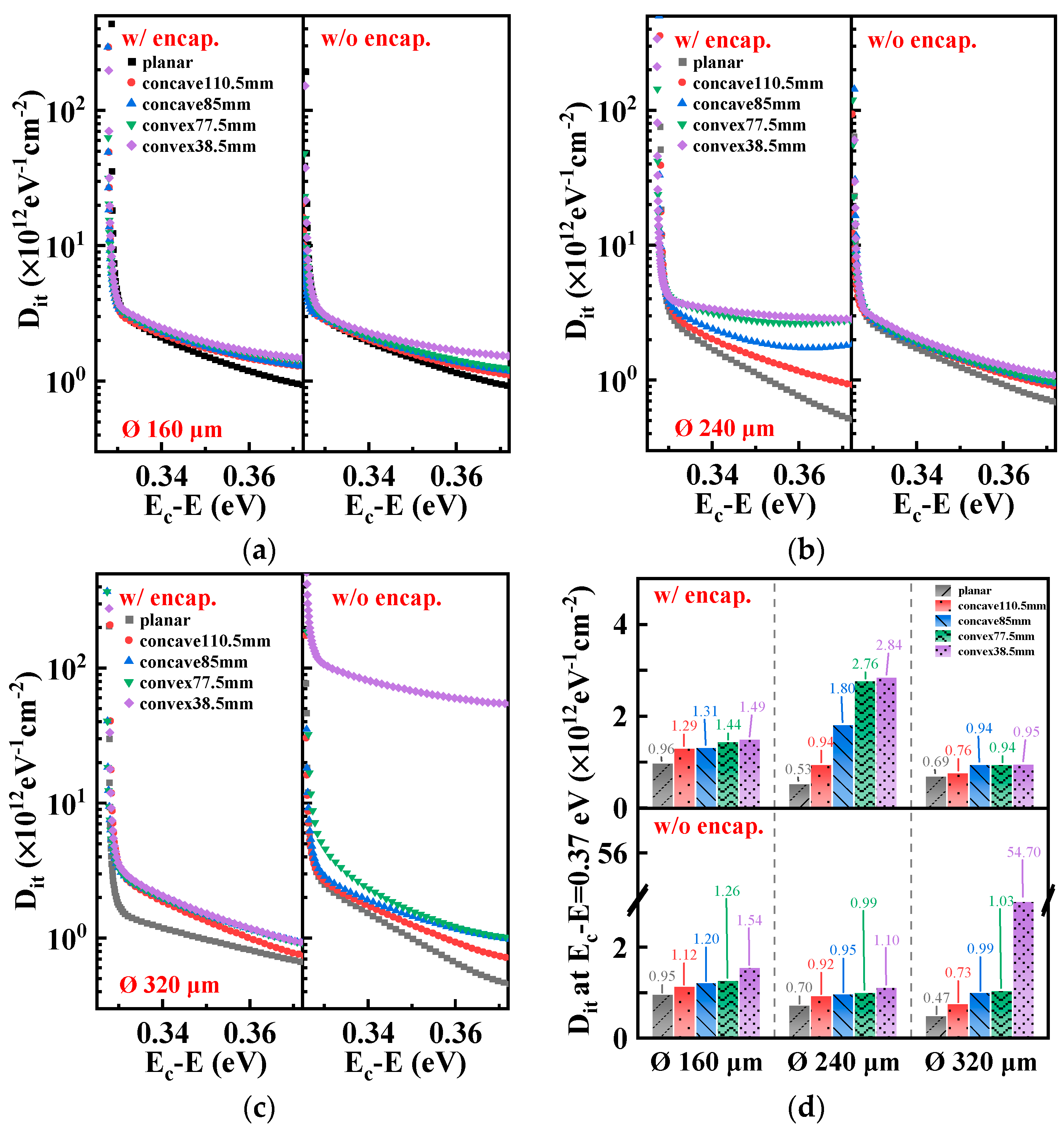
Figure 14a illustrates the Dit distribution for Al2O3/alucone encapsulated and bare MOSCAPs with Ø 160 μm under bending conditions. The Dit values were extracted by Terman methods [21]. The encapsulated MOSCAPs with Ø 160 μm exhibit almost similar changes in bending strains related to Dit distribution compared to the bare device with the same Ø of 160 μm, which is probably due to the optimized NMP position in the Si channel using ultrathin encapsulation strategies. When the Ø increased, the variations in Dit distribution differed at 240 μm and 320 μm, as shown in Figures 14b and 14c. For Ø 240 μm of encapsulated and bare MOSCAPs, the obvious increase in Dit according to bending strains is verified in the former. Yet, the relatively stable performance in the latter is due to the reliability of both Cmax and frequency dispersion. When the Ø further increased to 320 μm for bare MOSCAPs, the Dit values at investigated Ec-E entirely increased two orders of magnitude under high deformation of (+)38.5 mm. Hence, the encapsulated MOSCAPs with Ø 320 μm can maintain the stability of Dit distributions under bending conditions. Moreover, in encapsulated MOSCAPs with Ø 320 μm, Dit values distributed at 0.33 eV beneath the conduction band (Ec) at bending states notably increased to 2 times at the planar state.
Importantly, the Dit values for encapsulated and bare MOSCAPs with three types of Ø are representative at the energy level of Ec-E = 0.37 eV (i.e., 0.19 eV above midgap) that changed with different Ø under bending deformations, as shown in Figure 14(d). Compared to the planar state, the variations on Dit at the energy level of Ec-E = 0.37 eV of MOSCAPs with Ø 160 μm increased to 1.3, 1.4, 1.5, and 1.6 times in encapsulated devices at four bending radii. Yet, it increased to 1.2, 1.3, 1.3, and 1.6 times in bare devices corresponding to the same bending deformation. The variations are continually stable for larger Ø of 240 μm in bare MOSCAPs which increased to 1.3, 1.4, 1.4, and 1.6 times. But the values rose rapidly for the largest Ø of 320 μm in bare MOSCAPs which increased to 1.6, 2.1, 2.2, and 116.2 times under four bending conditions compared with the planar state. On the other hand, for encapsulated MOSCAPs with Ø 240 μm, the variations corresponding to the four bending states on Dit at the energy level of Ec-E = 0.37 eV increased to 1.8, 3.4, 5.3, and 5.4 times. The variations on Dit at reference energy level in encapsulated MOSCAPs with Ø 320 μm importantly and stably increased to 1.1, 1.4, 1.4, and 1.4 times under four bending conditions. From the thorough analysis of Dit results, it can be carefully speculated that the interfacial characteristics of MOSCAPs with different gate dielectric surface areas under bending deformations are promoted/maintained overall through ultrathin encapsulation strategies of Al2O3/alucone nanolaminates.
5. Conclusions
In conclusion, ultrathin encapsulation strategies of Al2O3/alucone nanolaminates combined with different gate dielectric surface areas were employed in flexible monocrystalline Si NM based MOSCAPs and the electrical properties of encapsulated MOSCAPs with different gate dielectric islands were explored and evaluated under the planar and different bending deformations. The circular gate dielectric surface areas equipped with three types of Ø at 160 μm, 240 μm, and 320 μm performed different mechanisms under bending conditions. For encapsulated MOSCAPs with Ø of 160 μm, it can maintain the stability on Cmax and frequency dispersion under concave and convex bending conditions, as well as have a certain ability to inhibit the growth of Jg compared to the bare MOSCAPs with the same Ø. As the Ø increased to Ø of 240 μm, it not only maintained the stability in Cmax but strengthened the reliability in Jg and Vfb, while the performances on frequency dispersion accompanied with interfacial properties under convex bending deformations were supposed to be further optimized. The interfacial characteristics were enhanced under concave and convex bending conditions for encapsulated MOSCAPs at the largest Ø of 320 μm. However, the Cmax deteriorated due to the high convex bending deformations the performances on Jg were decent in this configuration. These findings highlight that the different gate dielectric surface areas as form factors significantly influence the electrical performances in Si NM based MOSCAPs w/ and w/o encapsulation according to the concave and convex bending deformations. It is promising to use ultrathin encapsulation strategies to enhance the reliability and yields of high performance, long-lived flexible transistors based on ultrathin Si channel.
Author Contributions
Conceptualization, C.L. and Z.W.; Methodology, Z.W. and H.L.; Software, Z.W.; Formal analysis, Z.W.; Investigation, C.L. and Z.W.; Writing—original draft, Z.W. and C.L.; Writing—review and editing, Z.W. and C.L.; Supervision, Y.Z.; Project administration, C.L.; Funding acquisition, C.L. and H.L. All authors have read and agreed to the published version of the manuscript.
Funding
This research was funded by the National Natural Science Foundation of China (Grant No. 92164202), Fundamental Research Funds for the Central Universities (Grant No. QTZX23096), National Defense Science and Technology Foundation Strengthening Program (Grant No. 2019-XXXX-XX-236-00), and National Natural Science Foundation of China (Grant No. 61804116).
Data Availability Statement
Data are contained within the article.
Conflicts of Interest
The authors declare no conflicts of interest.
Appendix
References
- Mariello, M.; Kim, K.; Wu, K.; Lacour, S.P.; Leterrier, Y. Recent advances in encapsulation of flexible bioelectronic implants: materials, technologies, and characterization methods. Adv. Mater. 2022, 34, 2201129. [Google Scholar] [CrossRef] [PubMed]
- Cho, Y.; Park, S.; Lee, J.; Yu, K.J. Emerging materials and technologies with applications in flexible neural implants: a comprehensive review of current issues with neural devices. Adv. Mater. 2021, 33, 2005786. [Google Scholar] [CrossRef] [PubMed]
- Oldroyd, P.; Malliaras, G.G. Achieving long-term stability of thin-film electrodes for neurostimulation. Acta Biomater. 2022, 139, 65–81. [Google Scholar] [CrossRef] [PubMed]
- Sinha, S.; Pal, T. A comprehensive review of FET-based pH sensors: materials, fabrication technologies, and modeling. Electrochem. Sci. Adv. 2022, 2, e2100147. [Google Scholar] [CrossRef]
- Khau, B.V.; Scholz, A.D.; Reichmanis, E. Advances and opportunities in development of deformable organic electrochemical transistors. J. Mater. Chem. C 2020, 8, 15067–15078. [Google Scholar] [CrossRef]
- Lee, J.Y.; Shin, J.; Kim, K.; Ju, J.E.; Dutta, A.; Kim, T.S.; Cho, Y.U.; Kim, T.; Hu, L.; Min, W.K.; Jung, H.S.; Park, Y.S.; Won, S.M.; Yeo, W.H.; Moon, J.; Khang, D.Y.; Kim, H.J.; Ahn, J.H.; Cheng, H.; Yu, K.J.; Rogers, J.A. Ultrathin crystalline silicon nano and micro membranes with high areal density for low-cost flexible electronics. Small 2023, 19, 2302597. [Google Scholar] [CrossRef] [PubMed]
- Seo, K.J.; Hill, M.; Ryu, J.; Chiang, C.H.; Rachinskiy, I.; Qiang, Y.; Jang, D.; Trumpis, M.; Wang, C.; Viventi, J.; Fang, H. A soft, high-density neuroelectronic array. npj Flex. Electron. 2023, 7, 40. [Google Scholar] [CrossRef] [PubMed]
- Multia, J.; Karppinen, M. Atomic/Molecular layer deposition for designer’s functional metal–organic materials. Adv. Mater. Interfaces 2022, 9, 2200210. [Google Scholar] [CrossRef]
- Niemelä, J.P.; Rohbeck, N.; Michler, J.; Utke, I. Molecular layer deposited alucone thin films from long-chain organic precursors: from brittle to ductile mechanical characteristics. Dalton Trans. 2020, 49, 10832–10838. [Google Scholar] [CrossRef]
- Song, E.; Li, J.; Won, S.M.; Bai, W.; Rogers, J.A. Materials for flexible bioelectronic systems as chronic neural interfaces. Nat. Mater. 2020, 19, 590–603. [Google Scholar] [CrossRef]
- Zhao, Y.; Goncharova, L.V.; Zhang, Q.; Kaghazchi, P.; Sun, Q.; Lushington, A.; Wang, B.; Li, R.; Sun, X. Inorganic–organic coating via molecular layer deposition enables long life sodium metal anode. Nano Lett. 2017, 17, 5653–5659. [Google Scholar] [CrossRef]
- Han, Y.C.; Jeong, E.G.; Kim, H.; Kwon, S.; Im, H.G.; Bae, B.S.; Choi, K.C. Reliable thin-film encapsulation of flexible OLEDs and enhancing their bending characteristics through mechanical analysis. RSC Adv. 2016, 6, 40835–40843. [Google Scholar] [CrossRef]
- Fang, H.; Zhao, J.; Yu, K.J.; Song, E.; Farimani, A.B.; Chiang, C.H.; Jin, X.; Xue, Y.; Xu, D.; Du, W.; Seo, K.J.; Zhong, Y.; Yang, Z.; Won, S.M.; Fang, G.; Choi, S.W.; Chaudhuri, S.; Huang, Y.; Alam, M.A.; Viventi, J.; Aluru, N.R.; Rogers, J.A. Ultrathin, transferred layers of thermally grown silicon dioxide as biofluid barriers for biointegrated flexible electronic systems. Proc. Natl. Acad. Sci. U.S.A. 2016, 113, 11682–11687. [Google Scholar] [CrossRef]
- Fang, H.; Yu, K.J.; Gloschat, C.; Yang, Z.; Song, E.; Chiang, C.H.; Zhao, J.; Won, S.M.; Xu, S.; Trumpis, M.; Zhong, Y.; Han, S.W.; Xue, Y.; Xu, D.; Choi, S.W.; Cauwenberghs, G.; Kay, M.; Huang, Y.; Viventi, J.; Efimov, I.R.; Rogers, J.A. Capacitively coupled arrays of multiplexed flexible silicon transistors for long-term cardiac electrophysiology. Nat Biomed Eng. 2017, 1, 0038. [Google Scholar]
- Xiao, W.; Hui, D.Y.; Zheng, C.; Yu, D.; Qiang, Y.Y.; Ping, C.; Xiang, C.L.; Yi, Z. A flexible transparent gas barrier film employing the method of mixing ALD/MLD-grown Al2O3 and alucone layers. Nanoscale Res. Lett. 2015, 10, 130. [Google Scholar] [CrossRef]
- Hwang, B.; Qaiser, N.; Lee, C.; Matteini, P.; Yoo, S.J.; Kim, H. Effect of Al2O3/alucone nanolayered composite overcoating on reliability of Ag nanowire electrodes under bending fatigue. J. Alloy. Compd. 2020, 846, 156420. [Google Scholar] [CrossRef]
- Kim, S.Y.; Bong, J.H.; Kim, C.; Hwang, W.S.; Kim, T.S.; Cho, B.J. Mechanical stability analysis via neutral mechanical plane for high-performance flexible Si nanomembrane FDSOI device. Adv. Mater. Interfaces 2017, 4, 1700618. [Google Scholar] [CrossRef]
- Cao, K.; Chen, R.; Li, Y.; Xiong, Y.; Yang, H. Thin film encapsulation for the organic light-emitting diodes display via atomic layer deposition. J. Mater. Res. 2020, 35, 681–700. [Google Scholar]
- Bao, M. Analysis and design principles of MEMS devices, 1st ed; Elsevier Science: Amsterdam, Netherlands, 2005; pp. 54–59. [Google Scholar]
- Liu, C.; Wang, Z.; Zhang, Y.; Lü, H.; Zhang, Y.M. Nanolaminated HfO2/Al2O3 dielectrics for high-performance silicon nanomembrane based field-effect transistors on biodegradable substrates. Adv. Mater. Interfaces 2022, 9, 2201477. [Google Scholar] [CrossRef]
- Liu, C.; Zhang, Y.; Zhang, Y.M.; Lü, H.L. Interfacial characteristics of Al/Al2O3/ZnO/n-GaAs MOS capacitor. Chinese Physics B 2013, 22, 076701. [Google Scholar] [CrossRef]
- Cao, Y.; Allameh, S.; Nankivil, D.; Sethiaraj, S.; Otiti, T.; Soboyejo, W. Nanoindentation measurements of the mechanical properties of polycrystalline Au and Ag thin films on silicon substrates: Effects of grain size and film thickness. Mater. Sci. Eng. A 2006, 427, 232–240. [Google Scholar] [CrossRef]
- Park, S.I.; Ahn, J.H.; Feng, X.; Wang, S.; Huang, Y.; Rogers, J.A. Theoretical and experimental studies of bending of inorganic electronic materials on plastic substrates. Adv. Funct. Mater. 2008, 18, 2673–2684. [Google Scholar] [CrossRef]
- Chang, H.Y.; Yang, S.; Lee, J.; Tao, L.; Hwang, W.S.; Jena, D.; Lu, N.; Akinwande, D. High-performance, highly bendable MoS2 transistors with high-k dielectrics for flexible low-power systems. ACS Nano 2013, 7, 5446–5452. [Google Scholar] [CrossRef]
- Rontu, V.; Nolvi, A.; Hokkanen, A.; Haeggström, E.; Kassamakov, I.; Franssila, S. Elastic and fracture properties of free-standing amorphous ALD Al2O3 thin films measured with bulge test. Mater. Res. Express 2018, 5, 046411. [Google Scholar] [CrossRef]
- Berdova, M.; Liu, X.; Wiemer, C.; Lamperti, A.; Tallarida, G.; Cianci, E.; Fanciulli, M.; Franssila, S. Hardness, elastic modulus, and wear resistance of hafnium oxide-based films grown by atomic layer deposition. J. Vac. Sci. Technol. A 2016, 34, 051510. [Google Scholar] [CrossRef]
- Ruoho, M.; Tarasiuk, N.; Rohbeck, N.; Kapusta, C.; Michler, J.; Utke, I. Stability of mechanical properties of molecular layer–deposited alucone. Mater. Today Chem. 2018, 10, 187–194. [Google Scholar] [CrossRef]
Figure 1.
Cross-sectional schematic illustration of Al2O3/alucone encapsulated (upper) and bare (lower) MOSCAPs labeled with width dimensions and NMP positions.
Figure 1.
Cross-sectional schematic illustration of Al2O3/alucone encapsulated (upper) and bare (lower) MOSCAPs labeled with width dimensions and NMP positions.

Figure 2.
Maximum strain in the device layer, i.e., anode, HfO2/Al2O3 bilayered dielectric, and Si channel layer, changed as bending radii (Rb) for Al2O3/alucone encapsulated and bare MOSCAPs with different diameters (Ø).
Figure 2.
Maximum strain in the device layer, i.e., anode, HfO2/Al2O3 bilayered dielectric, and Si channel layer, changed as bending radii (Rb) for Al2O3/alucone encapsulated and bare MOSCAPs with different diameters (Ø).
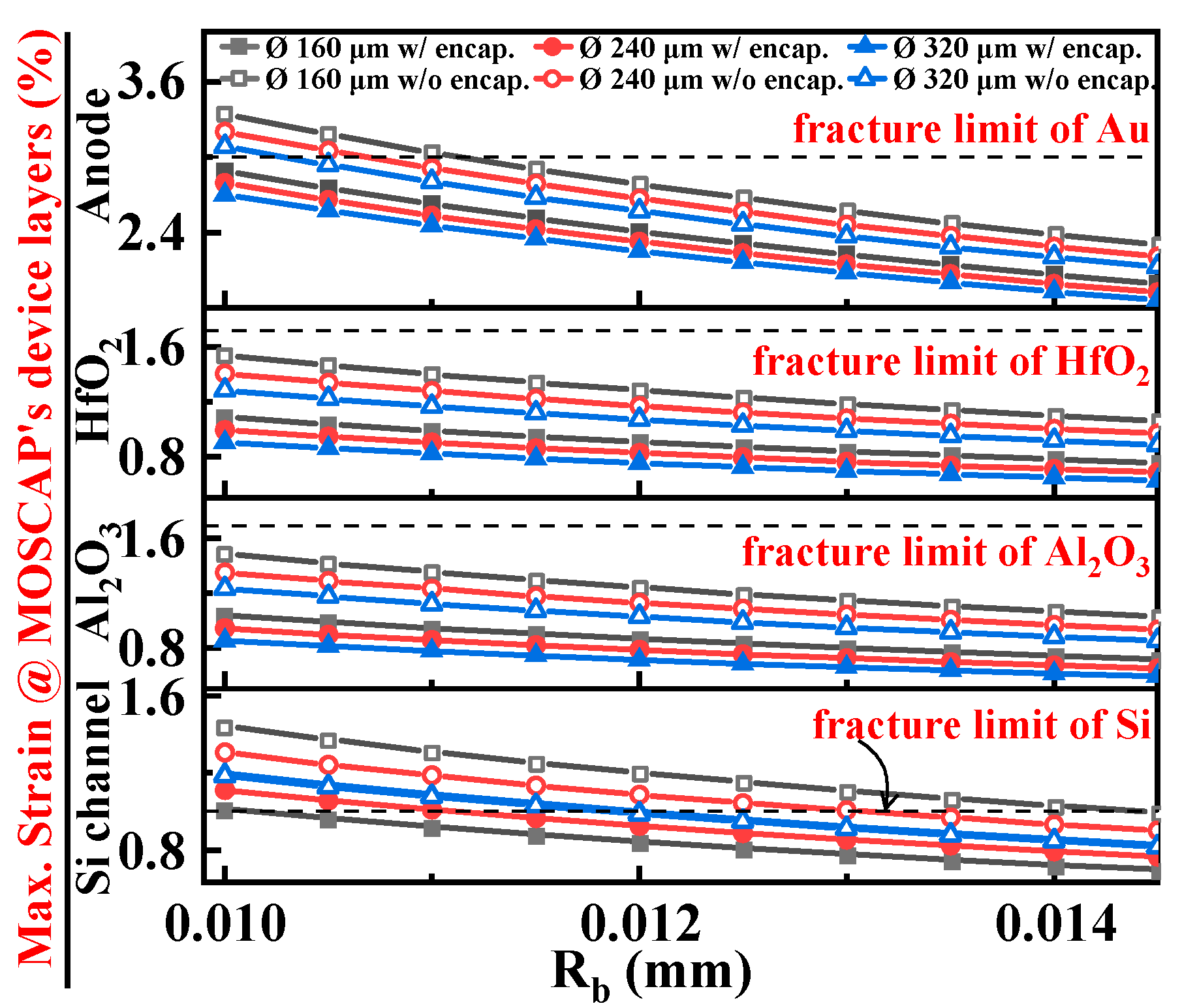
Figure 3.
C-V curves at the planar state obtained from encapsulated and bare MOSCAPs with different Ø. Inset: schematic illustration of encapsulated MOSCAPs on the bendable substrate.
Figure 3.
C-V curves at the planar state obtained from encapsulated and bare MOSCAPs with different Ø. Inset: schematic illustration of encapsulated MOSCAPs on the bendable substrate.
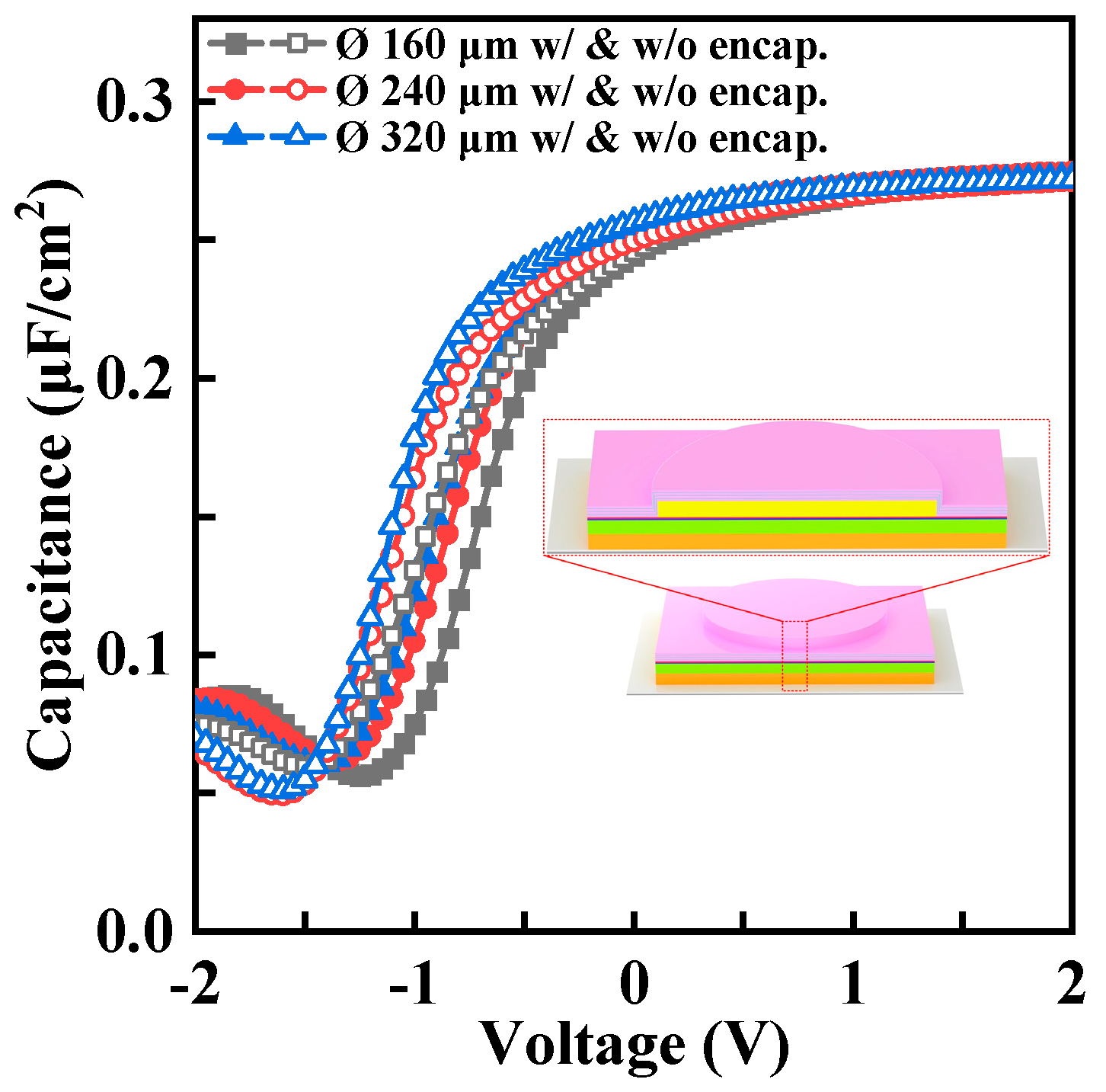
Figure 4.
J-V curves at the planar state obtained from encapsulated and bare MOSCAPs with different Ø.
Figure 4.
J-V curves at the planar state obtained from encapsulated and bare MOSCAPs with different Ø.
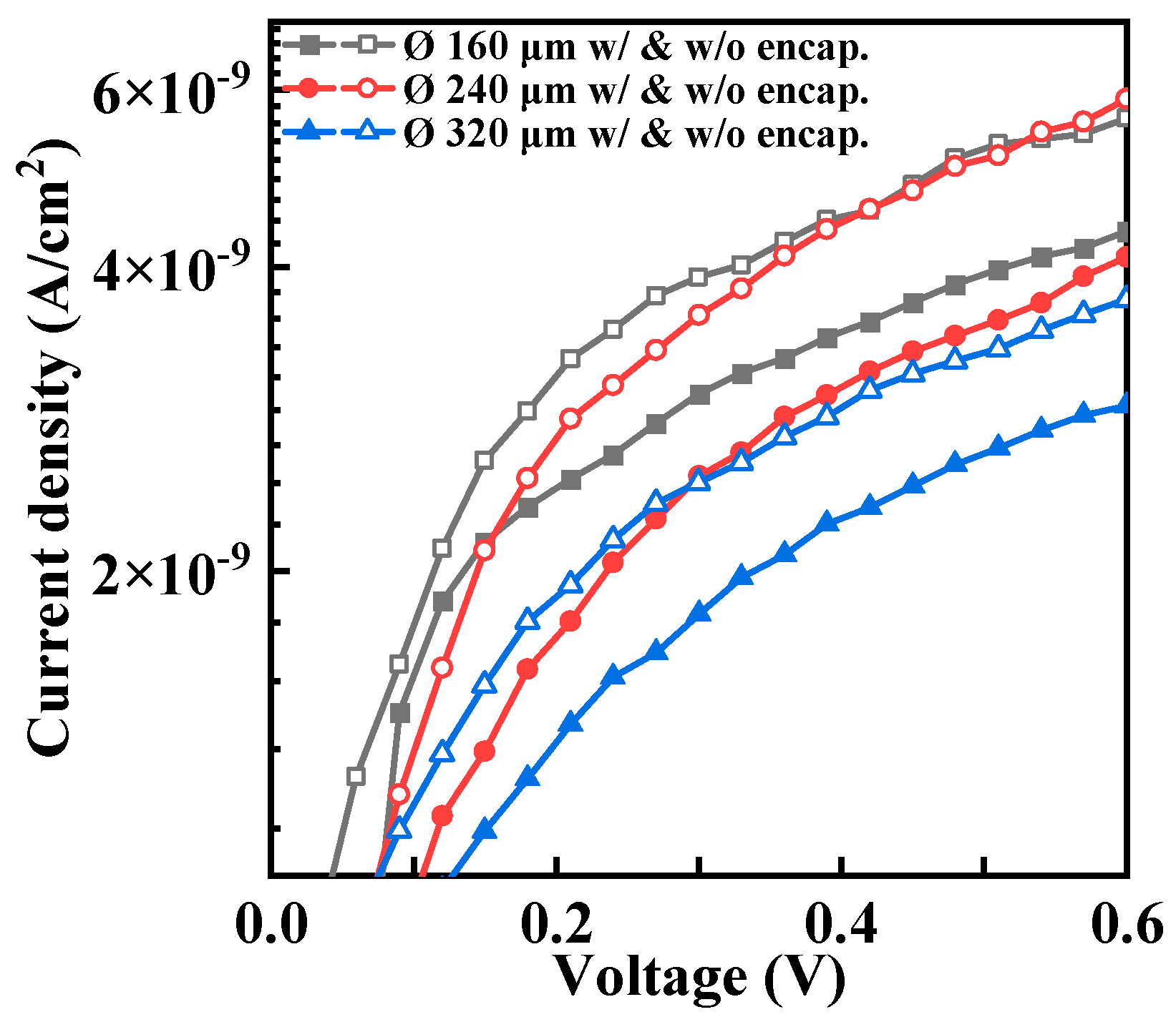
Figure 5.
C-V curves of MOSCAPs with Ø 160 μm under bending conditions. Inset: schematic illustration of encapsulated MOSCAPs bent inwardly and outwardly.
Figure 5.
C-V curves of MOSCAPs with Ø 160 μm under bending conditions. Inset: schematic illustration of encapsulated MOSCAPs bent inwardly and outwardly.
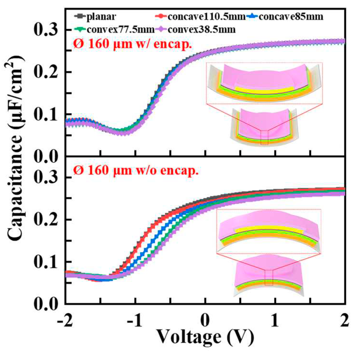
Figure 6.
C-V curves of circular MOSCAPs with Ø 240 μm under bending conditions.

Figure 7.
C-V curves of circular MOSCAPs with Ø 320 μm under bending conditions.
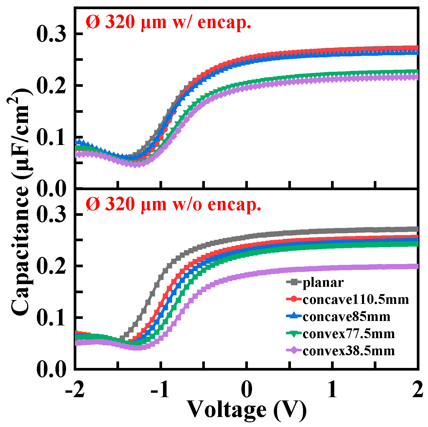
Figure 8.
The maximum capacitance (Cmax) changed as a function of Ø under bending conditions.
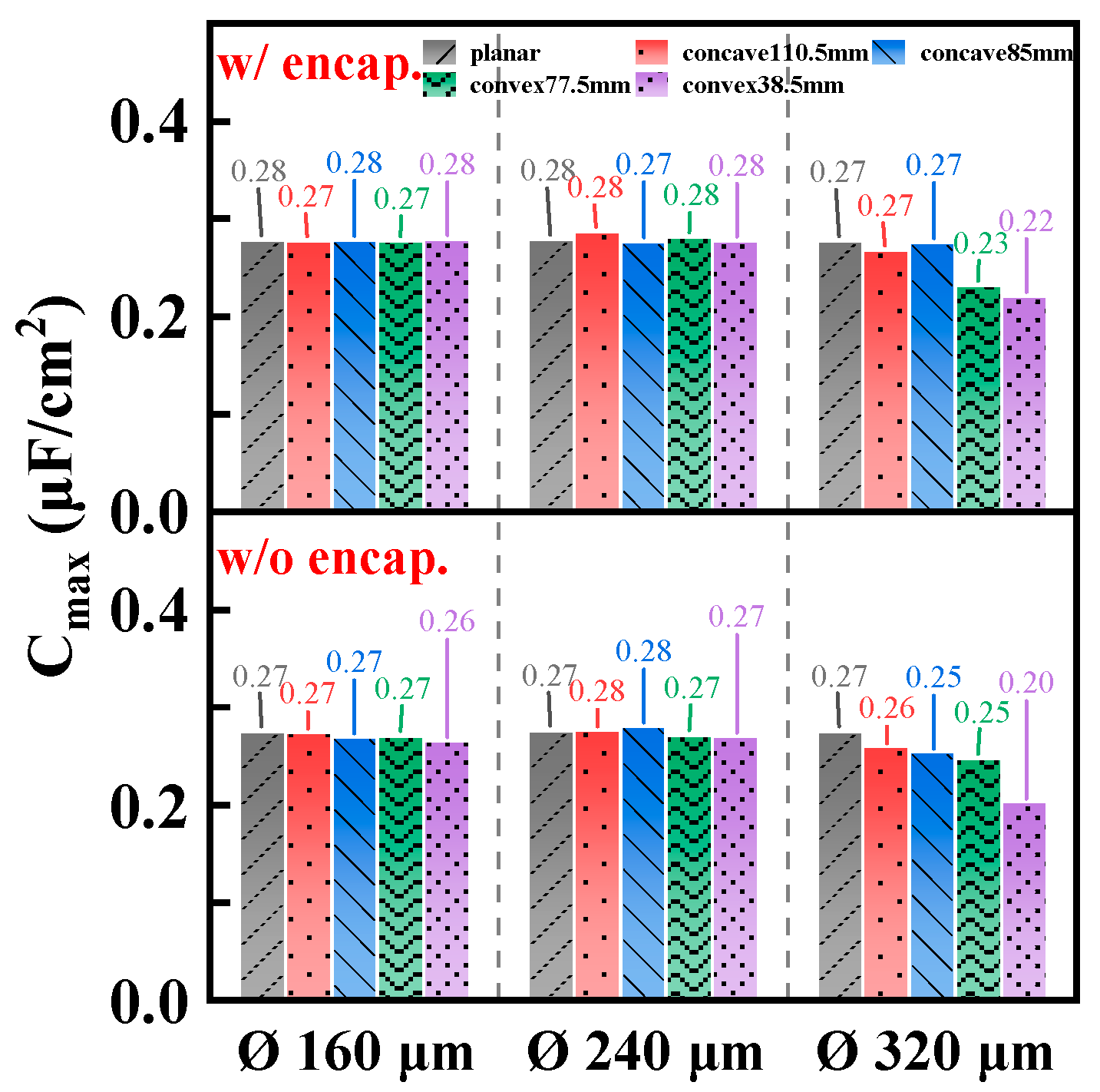
Figure 9.
J-V curves changed as a function of Ø under bending conditions.
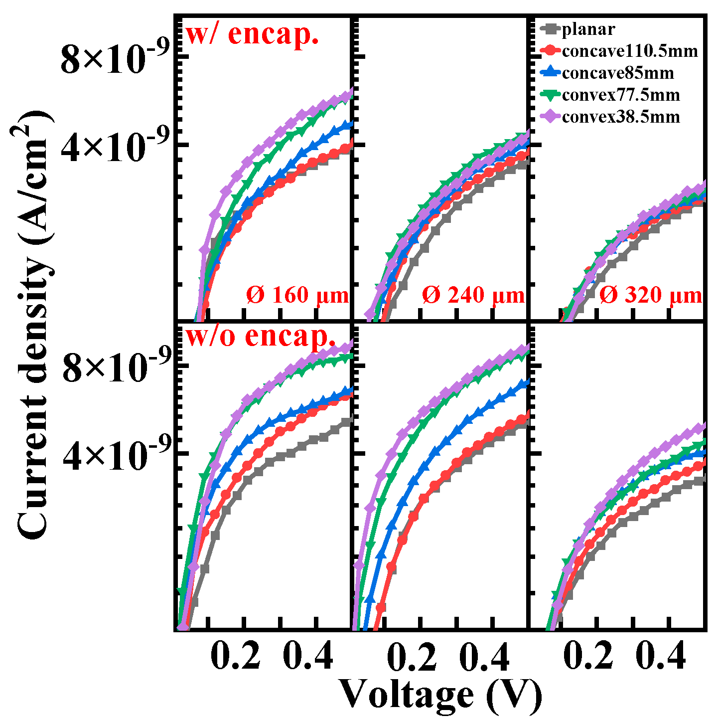
Figure 10.
The gate leakage current density (Jg) changed as a function of Ø under bending conditions.
Figure 10.
The gate leakage current density (Jg) changed as a function of Ø under bending conditions.
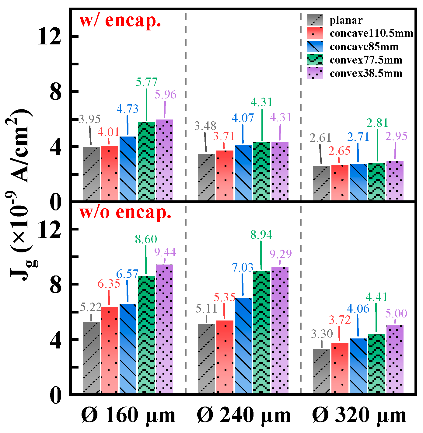
Figure 11.
(a) Vfb and (b) Neff changed as a function of Ø in MOSCAPs w/ and w/o encapsulation under bending conditions.
Figure 11.
(a) Vfb and (b) Neff changed as a function of Ø in MOSCAPs w/ and w/o encapsulation under bending conditions.
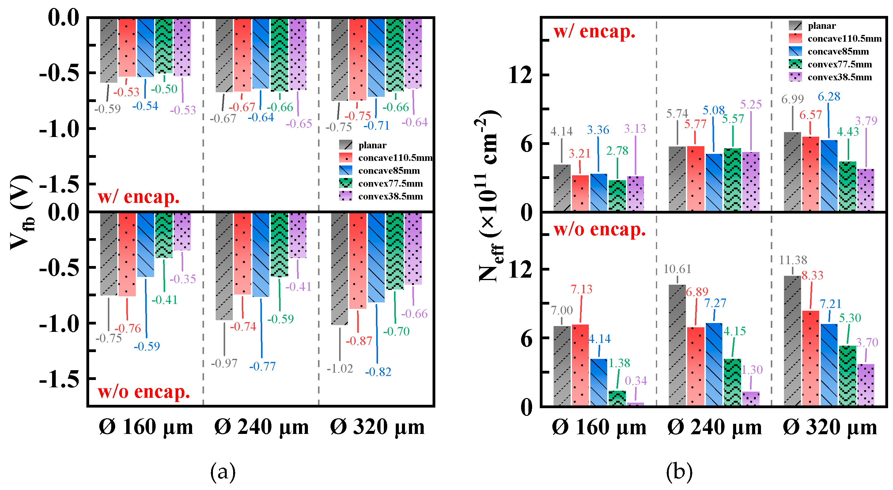
Figure 12.
Normalized Cmax versus frequency (ω) for encapsulated and bare MOSCAPs with three types of Ø.
Figure 12.
Normalized Cmax versus frequency (ω) for encapsulated and bare MOSCAPs with three types of Ø.
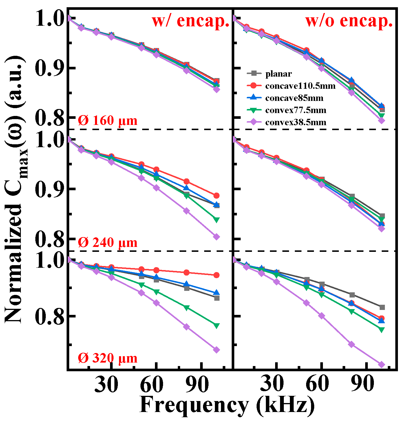
Figure 13.
Frequency dispersion in percentages per decade changed as a function of Ø under bending conditions.
Figure 13.
Frequency dispersion in percentages per decade changed as a function of Ø under bending conditions.
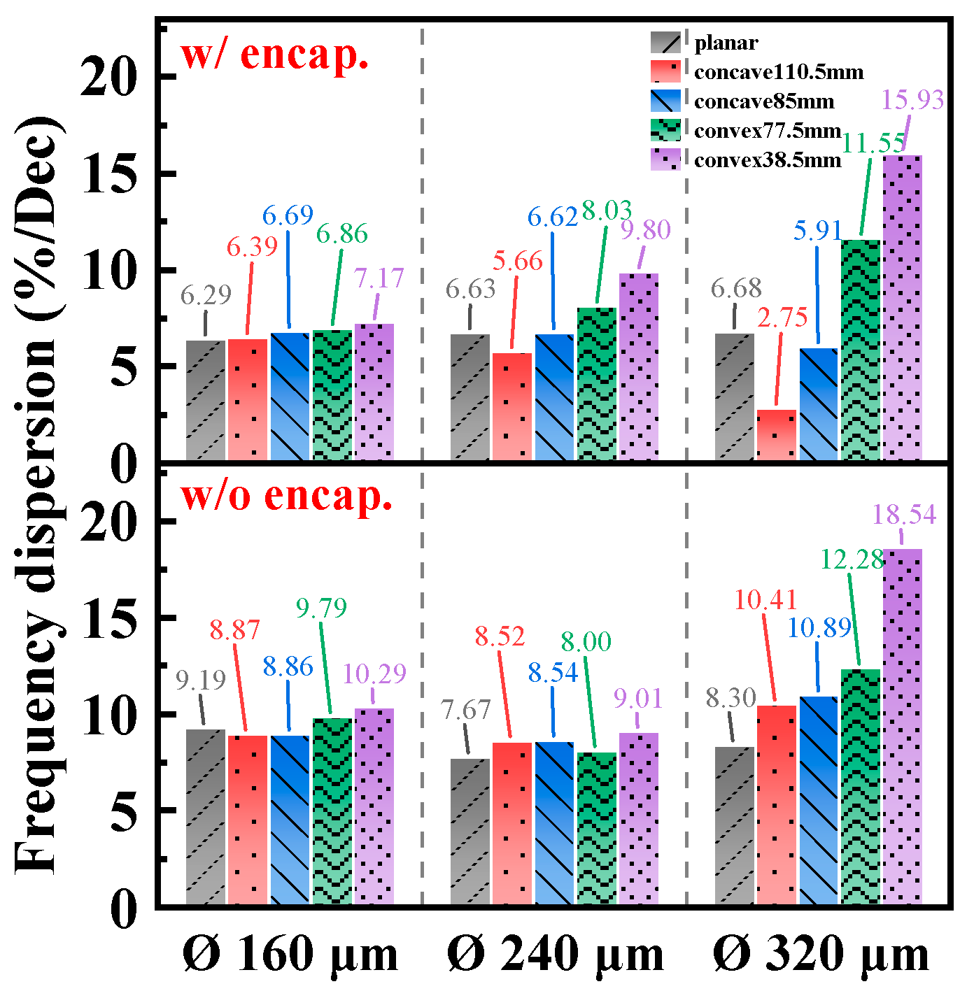
Figure 14.
Interface trap density (Dit) distribution changed with the energy level of Ec-E under bending conditions for encapsulated and bare MOSCAPs with Ø of (a) 160 μm, (b) 240 μm, and (c) 320 μm. (d) Dit corresponds to Ec-E at 0.37 eV changed as a function of Ø under bending conditions.
Figure 14.
Interface trap density (Dit) distribution changed with the energy level of Ec-E under bending conditions for encapsulated and bare MOSCAPs with Ø of (a) 160 μm, (b) 240 μm, and (c) 320 μm. (d) Dit corresponds to Ec-E at 0.37 eV changed as a function of Ø under bending conditions.
Disclaimer/Publisher’s Note: The statements, opinions and data contained in all publications are solely those of the individual author(s) and contributor(s) and not of MDPI and/or the editor(s). MDPI and/or the editor(s) disclaim responsibility for any injury to people or property resulting from any ideas, methods, instructions or products referred to in the content. |
© 2024 by the authors. Licensee MDPI, Basel, Switzerland. This article is an open access article distributed under the terms and conditions of the Creative Commons Attribution (CC BY) license (http://creativecommons.org/licenses/by/4.0/).
Copyright: This open access article is published under a Creative Commons CC BY 4.0 license, which permit the free download, distribution, and reuse, provided that the author and preprint are cited in any reuse.


